

NSC LM6325N, LM6225N Datasheet
LM6125/LM6225/LM6325
High Speed Buffer
General Description
The LM6125 family of high speed unity gain buffers slew at
800 V/µsand have a small signal bandwidth of 50 MHz while
driving a 50Ω load. These buffers drive
do not oscillate while driving large capacitive loads. The
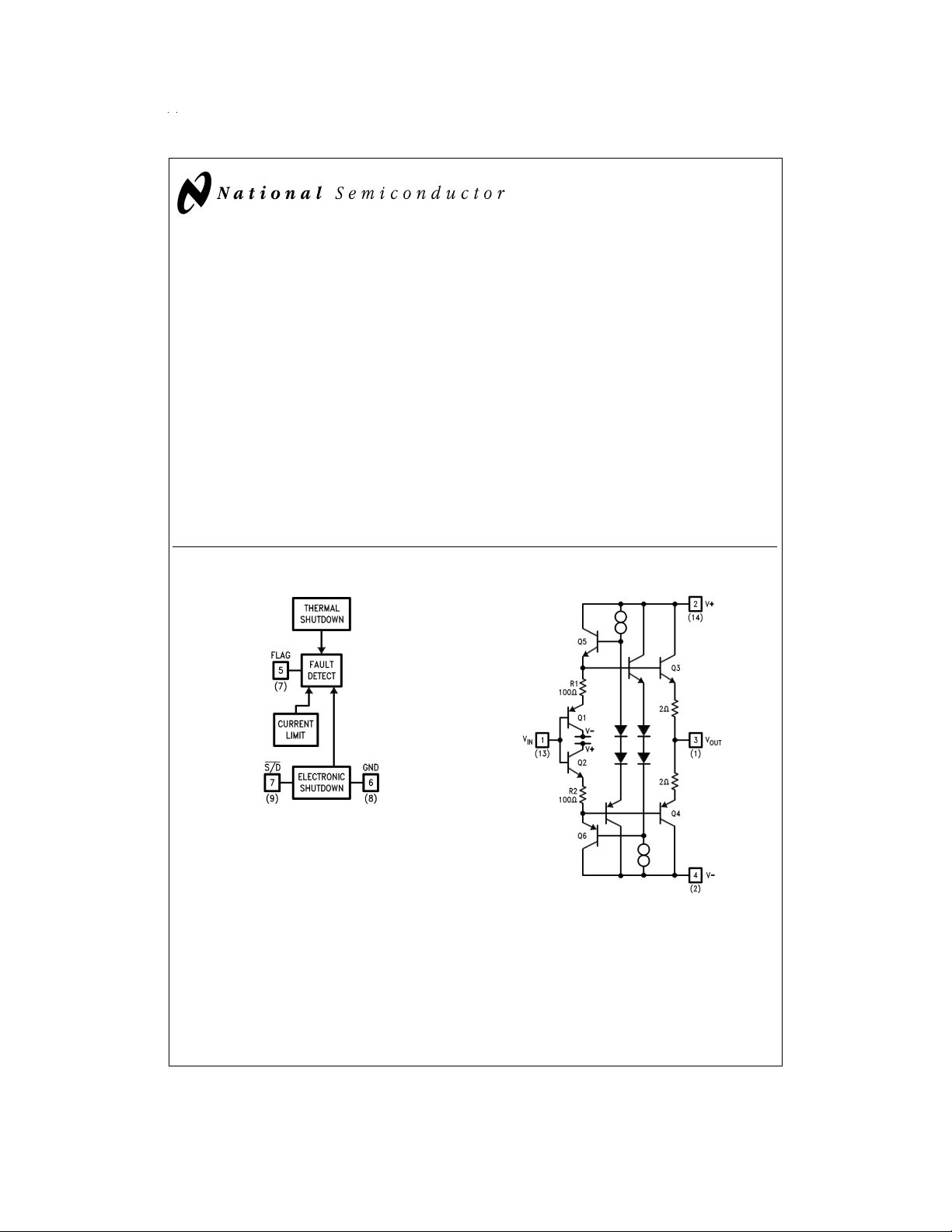
LM6125 contains unique features notfound inpower buffers;
these include current limit, thermal shutdown, electronic
shutdown, and an error flag that warns of fault conditions.
These buffers are built with National’s VIP
grated PNP) process which provides fast PNP transistors
that are true complements to the already fast NPN devices.
This advancedjunction-isolated process delivers high speed
performance without the need for complexand expensivedielectric isolation.
±
300 mA peak and
™
(Vertically Inte-
Features
n High slew rate: 800 V/µs
Simplified Schematic and Block Diagram
n High output current:
n Stable with large capacitive loads
n Current and thermal limiting
n Electronic shutdown
n 5V to
n Fully specified to drive 50Ω lines
Applications
n Line Driving
n Radar
n Sonar
±
300 mA
±
15V operation guaranteed
LM6125/LM6225/LM6325 High Speed Buffer
December 1994
DS009222-1
DS009222-2
Numbers in () are for 14–pin N DIP.
VIP™is a trademark of National Semiconductor Corporation.
© 1999 National Semiconductor Corporation DS009222 www.national.com
Pin Configurations
*Heat sinking pins.
Internally connected to V−.
Order Number LM6225N
See NS Package Number N14A
or LM6325N
DS009222-3
Note: Pin 4 connected to case
DS009222-4
Top View
Order Number LM6125H/883 (Note 1)
or LM6125H
See NS Package Number H08C
Note 1: Available per 5962-9081501
www.national.com 2
Absolute Maximum Ratings (Note 2)
If Military/Aerospace specified devices are required,
please contact the National Semiconductor Sales Office/
Distributors for availability and specifications.
Supply Voltage 36V (
Input to Output Voltage (Note 2)
Input Voltage
Output Short-Circuit to GND
(Note 3) Continuous
Flag Output Voltage GND ≤ Vflag ≤ +Vsupply
Storage Temperature Range −65˚C to +150˚C
Lead Temperature
(Soldering, 10 seconds) 260˚C
±
±
Vsupply
18V)
±
7V
ESD Tolerance (Note 9)
(Note 4)
θ
JA
±
H Package 150˚C/W
N Package 40˚C/W
Maximum Junction
Temperature (T
) 150˚C
J
Operating Temperature Range
LM6125 −55˚C to +125˚C
LM6225 −40˚C to +85˚C
LM6325 0˚C to +70˚C
Operating Supply Voltage Range 4.75V to
1500V
±
16V
DC Electrical Characteristics
=
The following specifications apply for Supply Voltage
Boldface limits apply for T
=
=
T
A
to T
T
J
MIN
MAX
±
15V, V
; all other limits T
Symbol Parameter Conditions Typ LM6125 LM6225 LM6325 Units
OUT
=
L
=
L
=
L
=
IN
=
L
=
L
=
L
=
=
L
=
L
=
L
A
A
A
Voltage Gain 1 R
V1
Voltage Gain 2 R
V2
Voltage Gain 3 R
V3
(Note 6) V
V
I
R
C
R
I
I
I
Offset Voltage R
OS
Input Bias Current R
B
Input Resistance R
IN
Input Capacitance 3.5 pF
IN
Output Resistance I
O
Supply Current 1 R
S1
Supply Current 2 R
S2
Supply Current R
S/D
=
±
1kΩ,V
50Ω,V
10V 0.990 0.980 0.980 0.970
IN
=
±
10V 0.900 0.860 0.860 0.850 V/V
IN
50Ω,V+=5V 0.840 0.780 0.780 0.750
(1.5 VPP) 0.750 0.700 0.700
2V
PP
1kΩ 15 30 30 50 mV
1kΩ,R
=
10 kΩ 14 45µA
S
50Ω 5MΩ
±
10 mA 3 5 5 5 Ω
∞
∞
,V+=5V 14 16 16 18 mA
∞
±=±
,V
15V 1.1 1.5 1.5 1.5
in Shutdown 2.0 2.0 2.0
V
V
V
V
Output Swing 1 R
O1
Output Swing 2 R
O2
Output Swing 3 R
O3
Output Swing 4 R
O4
=
1kΩ 13.5 13.3 13.3 13.2
L
=
100Ω 12.7 11.5 11.5 11
L
=
50Ω 12 11 11 10
L
=
50Ω 1.8 1.6 1.6 1.6 V
L
PSRR Power Supply V+=5V (Note 6) 70 60 60 60 dB
Rejection Ratio 55 50 50 Min
V
Flag Pin Output V
OL
Low Voltage V
±=±
5V to±15V 300 300 340 mV
=
0V 400 400 400 Max
S/D
=
≥ 100 kΩ and R
0, R
CM
L
=
=
T
25˚C.
A
J
=
50Ω unless otherwise noted.
S
Limit Limit Limit
(Notes 5, 10) (Note 5) (Note 5)
0.970 0.950 0.950
0.800 0.820 0.820 Min
50 60 100 Max
777Max
10 10 6 Max
15 18 18 20
20 20 22
18 18 20 Max
13 13 13
10 10 10 Min
999
1.3 1.4 1.5 Min
±
PP
V
www.national.com3
 Loading...