

NSC LM629N-8, LM629N-6, LM629MX-8, LM629M-8, LM629M-6 Datasheet
LM628/LM629
Precision Motion Controller
General Description
The LM628/LM629 are dedicated motion-control processors
designed for use with a variety of DC and brushless DC
servo motors, and other servomechanisms which provide a
quadrature incremental position feedback signal. The parts
perform theintensive, real-time computational tasks required
for high performance digital motion control. The host control
software interface is facilitated by a high-level command set.
The LM628 has an 8-bit output which can drive either an
8-bit or a 12-bit DAC. The components required to build a
servo system are reduced to the DC motor/actuator, an incremental encoder, a DAC, a power amplifier, and the
LM628. An LM629-based system is similar, except that it
provides an 8-bit PWM output for directly driving H-switches.
The parts are fabricated in NMOS and packaged in a 28-pin
dual in-line package or a 24-pin surface mount package
(LM629 only). Both 6 MHz and 8 MHz maximum frequency
versions are available with the suffixes -6 and -8, respectively, used to designate the versions. They incorporate an
SDA core processor and cells designed by SDA.
Features
n 32-bit position, velocity, and acceleration registers
n Programmable digital PID filter with 16-bit coefficients
n Programmable derivative sampling interval
n 8- or 12-bit DAC output data (LM628)
n 8-bit sign-magnitude PWM output data (LM629)
n Internal trapezoidal velocity profile generator
n Velocity, target position, and filter parameters may be
changed during motion
n Position and velocity modes of operation
n Real-time programmable host interrupts
n 8-bit parallel asynchronous host interface
n Quadrature incremental encoder interface with index
pulse input
n Available in a 28-pin dual in-line package or a 24-pin
surface mount package (LM629 only)
TRI-STATE®is a registered trademark of National Semiconductor Corporation.
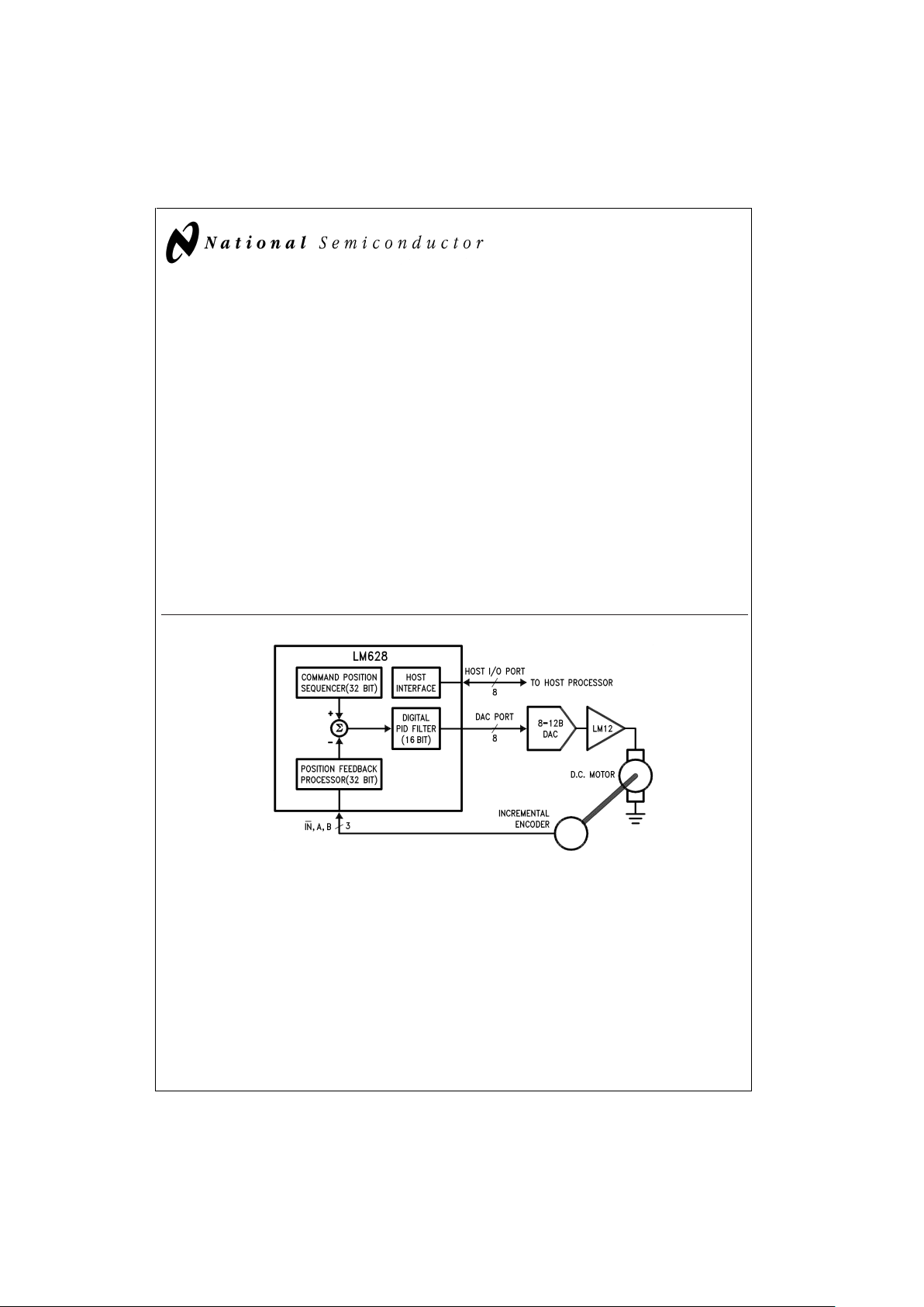
DS009219-1
FIGURE 1. Block Diagram
November 1999
LM628/LM629 Precision Motion Controller
© 1999 National Semiconductor Corporation DS009219 www.national.com
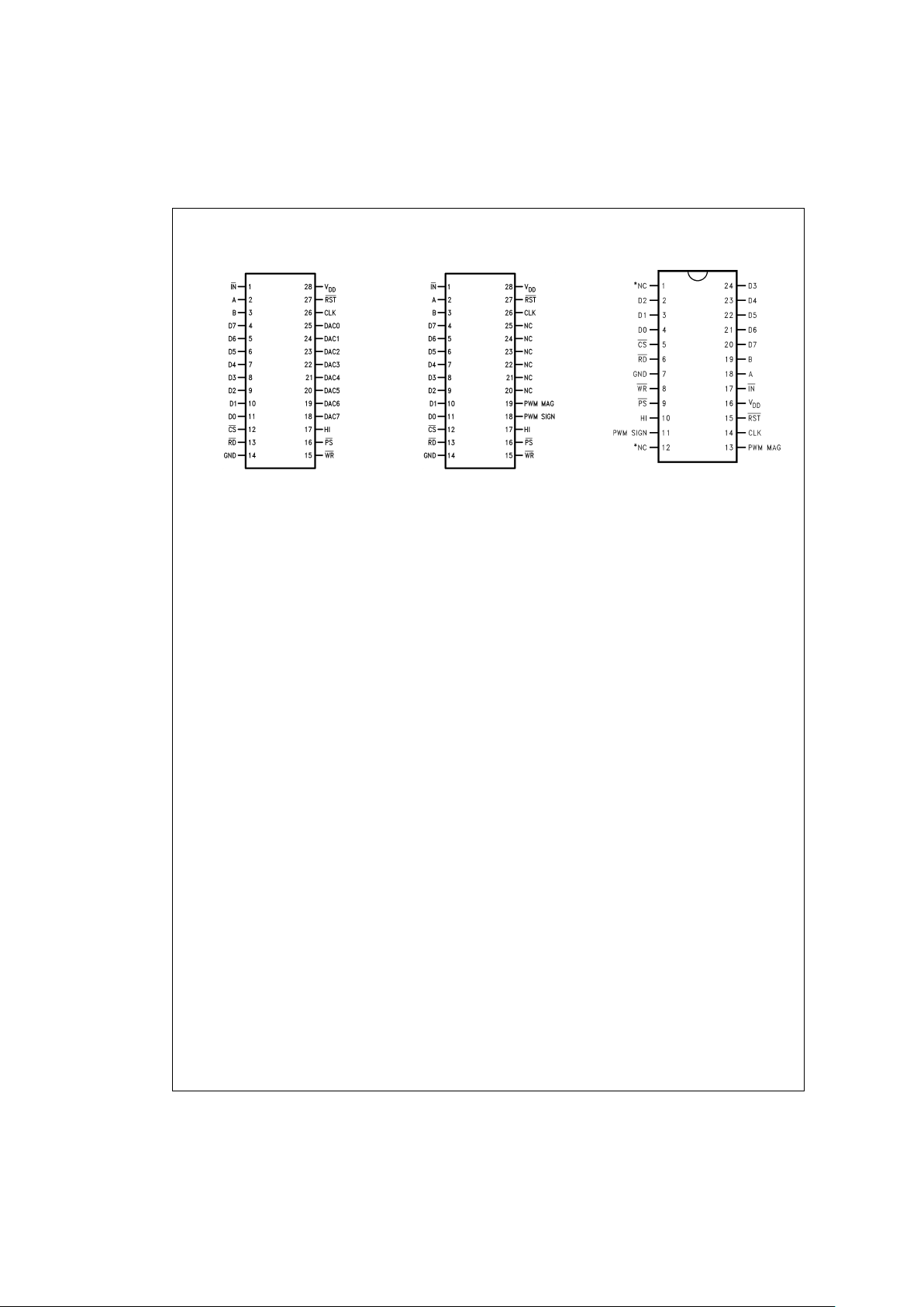
Connection Diagrams
LM628N
DS009219-2
LM629N
DS009219-3
LM629M
DS009219-21
*Do not connect.
Order Number LM629M-6, LM629M-8, LM628N-6, LM628N-8, LM629N-6 or LM629N-8
See NS Package Number M24B or N28B
LM628/LM629
www.national.com 2
Absolute Maximum Ratings (Note 1)
If Military/Aerospace specified devices are required,
please contact the National Semiconductor Sales Office/
Distributors for availability and specifications.
Voltage at Any Pin with
Respect to GND −0.3V to +7.0V
Ambient Storage Temperature −65˚C to +150˚C
Lead Temperature
28-pin Dual In-Line
Package (Soldering, 4 sec.) 260˚C
24-pin Surface Mount
Package (Soldering, 10 sec.) 300˚C
Maximum Power Dissipation
(T
A
≤ 85˚C, (Note 2) 605 mW
ESD Tolerance
(C
ZAP
=
120 pF, R
ZAP
=
1.5k) 2000V
Operating Ratings
Temperature Range −40˚C<T
A
<
+85˚C
Clock Frequency:
LM628N-6, LM629N-6,
LM629M-6 1.0 MHz
<
f
CLK
<
6.0 MHz
LM628N-8, LM629N-8,
LM629M-8 1.0 MHz
<
f
CLK
<
8.0 MHz
V
DD
Range 4.5V<V
DD
<
5.5V
DC Electrical Characteristics
(VDDand TAper Operating Ratings; f
CLK
=
6 MHz)
Symbol Parameter Conditions Tested Limits Units
Min Max
I
DD
Supply Current Outputs Open 110 mA
INPUT VOLTAGES
V
IH
Logic 1 Input Voltage 2.0 V
V
IL
Logic 0 Input Voltage 0.8 V
I
IN
Input Currents 0 ≤ VIN≤ V
DD
−10 10 µA
OUTPUT VOLTAGES
V
OH
Logic 1 I
OH
=
−1.6 mA 2.4 V
V
OL
Logic 0 I
OL
=
1.6 mA 0.4 V
I
OUT
TRI-STATE®Output Leakage Current 0 ≤ V
OUT
≤ V
DD
−10 10 µA
AC Electrical Characteristics
(VDDand TAper Operating Ratings; f
CLK
=
6 MHz; C
LOAD
=
50 pF; Input Test Signal t
r
=
t
f
=
10 ns)
Timing Interval T
#
Tested Limits Units
Min Max
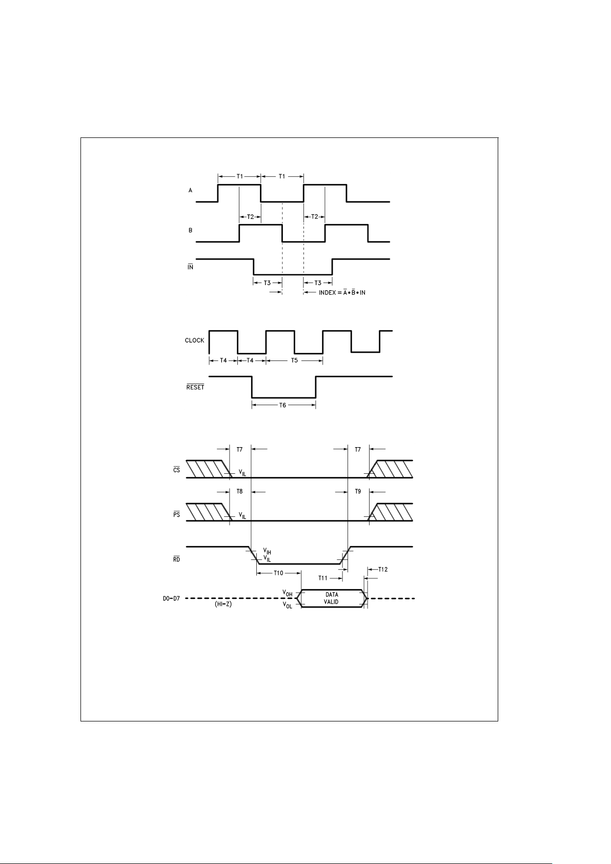
ENCODER AND INDEX TIMING (See
Figure 2
)
Motor-Phase Pulse Width T1
µs
Dwell-Time per State T2
µs
Index Pulse Setup and Hold T3 0 µs
(Relative to A and B Low)
CLOCK AND RESET TIMING (See
Figure 3
)
Clock Pulse Width
LM628N-6, LM629N-6, LM629M-6 T4 78 ns
LM628N-8, LM629N-8, LM629M-8 T4 57 ns
Clock Period
LM628N-6, LM629N-6, LM629M-6 T5 166 ns
LM628N-8, LM629N-8, LM629M-8 T5 125 ns
Reset Pulse Width T6
µs
LM628/LM629
www.national.com3
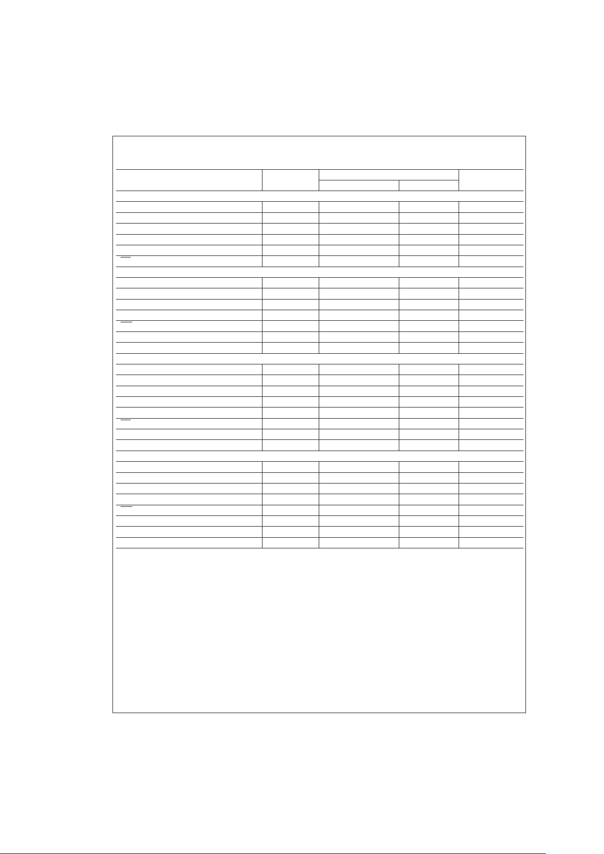
AC Electrical Characteristics (Continued)
(VDDand TAper Operating Ratings; f
CLK
=
6 MHz; C
LOAD
=
50 pF; Input Test Signal t
r
=
t
f
=
10 ns)
Timing Interval T
#
Tested Limits Units
Min Max
STATUS BYTE READ TIMING (See
Figure 4
)
Chip-Select Setup/Hold Time T7 0 ns
Port-Select Setup Time T8 30 ns
Port-Select Hold Time T9 30 ns
Read Data Access Time T10 180 ns
Read Data Hold Time T11 0 ns
RD High to Hi-Z Time
T12 180 ns
COMMAND BYTE WRITE TIMING (See
Figure 5
)
Chip-Select Setup/Hold Time T7 0 ns
Port-Select Setup Time T8 30 ns
Port-Select Hold Time T9 30 ns
Busy Bit Delay T13 (Note 3) ns
WR Pulse Width
T14 100 ns
Write Data Setup Time T15 50 ns
Write Data Hold Time T16 120 ns
DATA WORD READ TIMING (See
Figure 6
)
Chip-Select Setup/Hold Time T7 0 ns
Port-Select Setup Time T8 30 ns
Port-Select Hold Time T9 30 ns
Read Data Access Time T10 180 ns
Read Data Hold Time T11 0 ns
RD High to Hi-Z Time
T12 180 ns
Busy Bit Delay T13 (Note 3) ns
Read Recovery Time T17 120 ns
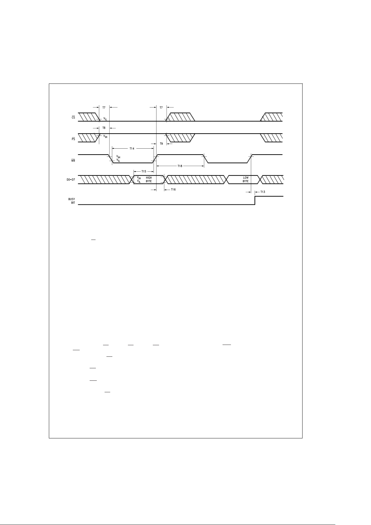
DATA WORD WRITE TIMING (See
Figure 7
)
Chip-Select Setup/Hold Time T7 0 ns
Port-Select Setup Time T8 30 ns
Port-Select Hold Time T9 30 ns
Busy Bit Delay T13 (Note 3) ns
WR Pulse Width
T14 100 ns
Write Data Setup Time T15 50 ns
Write Data Hold Time T16 120 ns
Write Recovery Time T18 120 ns
Note 1: Absolute Maximum Ratings indicate limits beyond which damage to the device may occur. DC and AC electrical specifications do not apply when operating
the device beyond the above Operating Ratings.
Note 2: When operating at ambient temperatures above 70˚C, the device must be protected against excessive junction temperatures. Mounting the package on a
printed circuit board having an area greater than three square inches and surrounding the leads and body with wide copper traces and large, uninterrupted areas of
copper, such as a ground plane, suffices. The 28-pin DIP (N) and the 24-pin surface mount package (M) are molded plastic packages with solid copper lead frames.
Most of the heat generated at the die flows from the die, through the copper lead frame, and into copper traces on the printed circuit board. The copper traces act
as a heat sink. Double-sided or multi-layer boards provide heat transfer characteristics superior to those of single-sided boards.
Note 3: In order to read the busy bit, the status byte must first be read. The time required to read the busy bit far exceeds the time the chip requires to set the busy
bit. It is, therefore, impossible to test actual busy bit delay. The busy bit is guaranteed to be valid as soon as the user is able to read it.
LM628/LM629
www.national.com 4
AC Electrical Characteristics (Continued)
DS009219-4
FIGURE 2. Quadrature Encoder Input Timing
DS009219-5
FIGURE 3. Clock and Reset Timing
DS009219-6
FIGURE 4. Status Byte Read Timing
LM628/LM629
www.national.com5
AC Electrical Characteristics (Continued)
DS009219-7
FIGURE 5. Command Byte Write Timing
DS009219-8
FIGURE 6. Data Word Read Timing
LM628/LM629
www.national.com 6
AC Electrical Characteristics (Continued)
Pinout Description
(See Connection Diagrams) Pin numbers for the 24-pin surface mount package are indicated in parentheses.
Pin 1 (17), Index (IN) Input: Receives optional index pulse
from the encoder. Must be tied high if not used. The index
position is read when Pins 1, 2, and 3 are low.
Pins 2 and 3 (18 and 19), Encoder Signal (A, B) Inputs:
Receive the two-phase quadrature signals provided by the
incremental encoder. When the motor is rotating in the positive (“forward”) direction, the signal at Pin 2 leads the signal
at Pin 3 by 90 degrees. Note that the signals at Pins 2 and 3
must remain at each encoder state (See
Figure 9
) for a minimum of 8 clock periods in order to be recognized. Because
of a four-to-one resolution advantage gained by the method
of decoding the quadrature encoder signals, this corresponds to a maximum encoder-state capture rate of 1.0 MHz
(f
CLK
=
8.0 MHz) or 750 kHz (f
CLK
=
6.0 MHz). For other
clock frequencies the encoder signals must also remain at
each state a minimum of 8 clock periods.
Pins 4 to 11 (20 to 24 and 2 to 4), Host I/O Port (D0 to D7):
Bi-directional data port which connects to host computer/
processor. Used for writing commands and data to the
LM628, and for reading the status byte and data from the
LM628, as controlled by CS (Pin 12), PS (Pin 16), RD (Pin
13), and WR (Pin 15).
Pin 12 (5), Chip Select (CS ) Input: Used to select the
LM628 for writing and reading operations.
Pin 13 (6), Read (RD ) Input: Used to read status and data.
Pin 14 (7), Ground (GND): Power-supply return pin.
Pin 15 (8), Write (WR ) Input: Used to write commands and
data.
Pin 16 (9), Port Select (PS ) Input: Used to select com-
mand or data port. Selects command port when low, data
port when high. The following modes are controlled by Pin
16:
1. Commands are written to the command port (Pin 16
low),
2. Status byte is read from command port (Pin 16 low), and
3. Data is written and read via the data port (Pin 16 high).
Pin 17 (10), Host Interrupt (HI) Output: This active-high
signal alerts the host (via a host interrupt service routine)
that an interrupt condition has occurred.
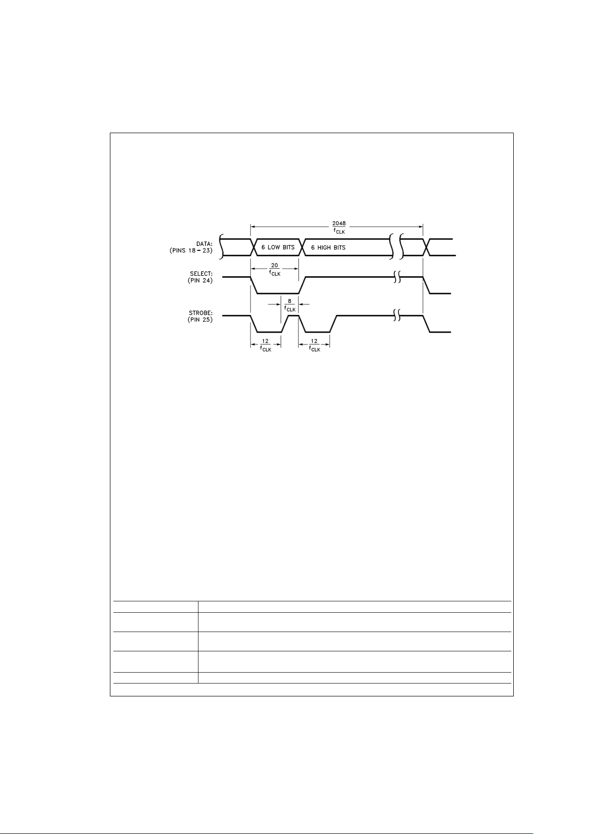
Pins 18 to 25, DAC Port (DAC0 to DAC7): Output port
which is used in three different modes:
1. LM628 (8-bit output mode): Outputs latched data to the
DAC. The MSB is Pin 18 and the LSB is Pin 25.
2. LM628 (12-bit output mode): Outputs two, multiplexed
6-bit words. The less-significant word is output first. The
MSB is on Pin 18 and the LSB is on Pin 23. Pin 24 is
used to demultiplex the words; Pin 24 is low for the
less-significant word. The positive-going edge of the signal on Pin 25 is used to strobe the output data.
Figure 8
shows the timing of the multiplexed signals.
3. LM629 (sign/magnitude outputs): Outputs a PWM sign
signal on Pin 18 (11 for surface mount), and a PWM
magnitude signal on Pin 19 (13 for surface mount). Pins
20 to 25 are not used in the LM629.
Figure 11
shows the
PWM output signal format.
Pin 26 (14), Clock (CLK) Input: Receives system clock.
Pin 27 (15), Reset (RST) Input: Active-low, positive-edge
triggered, resets the LM628 to the internal conditions shown
below. Note that the reset pulse must be logic low for a minimum of 8 clock periods. Reset does the following:
1. Filter coefficient and trajectory parameters are zeroed.
2. Sets position error threshold to maximum value (7FFF
hex), and effectively executes command LPEI.
3. The SBPA/SBPR interrupt is masked (disabled).
4. The five other interrupts are unmasked (enabled).
5. Initializes current position to zero, or “home” position.
6. Sets derivative sampling interval to 2048/f
CLK
or 256 µs
for an 8.0 MHz clock.
7. DAC port outputs 800 hex to “zero” a 12-bit DAC and
then reverts to 80 hex to “zero” an 8-bit DAC.
DS009219-9
FIGURE 7. Data Word Write Timing
LM628/LM629
www.national.com7
Pinout Description (Continued)
Immediately after releasing the reset pin from the LM628,
the status port should read “00”. If the reset is successfully
completed, the status word will change to hex “84” or “C4”
within 1.5 ms. If the status word has not changed from hex
“00” to “84” or “C4” within 1.5 ms, perform another reset and
repeat the above steps. To be certain that the reset was
properly performed, execute a RSTI command. If the chip
has reset properly, the status byte will change from hex “84”
or “C4” to hex “80” or “C0”. If this does not occur, perform another reset and repeat the above steps.
Pin 28 (16), Supply Voltage (V
DD
): Power supply voltage
(+5V).
Theory of Operation
INTRODUCTION
The typical system block diagram (See
Figure 1
) illustrates a
servo system built using the LM628. The host processor
communicates with the LM628 through an I/O port to facilitate programming a trapezoidal velocity profile and a digital
compensation filter. The DAC output interfaces to an external digital-to-analog converter to produce the signal that is
power amplified and applied to the motor.An incremental encoder provides feedback for closing the position servo loop.
The trapezoidal velocity profile generator calculates the required trajectory for either position or velocity mode of operation. In operation, the LM628 subtracts the actual position
(feedback position) from the desired position (profile generator position), and the resulting position error is processed by
the digital filter to drive the motor to the desired position.
Table1
provides a brief summary of specifications offered by
the LM628/LM629:
POSITION FEEDBACK INTERFACE
The LM628 interfaces to a motor via an incremental encoder.
Three inputs are provided: two quadrature signal inputs, and
an index pulse input. The quadrature signals are used to
keep track of the absolute position of the motor. Each time a
logic transition occurs at one of the quadrature inputs, the
LM628 internal position register is incremented or decremented accordingly. This provides four times the resolution
over the number of lines provided by the encoder. See
Fig-
ure 9
. Each of the encoder signal inputs is synchronized with
the LM628 clock.
The optional index pulse output provided by some encoders
assumes the logic-low state once per revolution. If the
LM628 is so programmed by the user, it will record the absolute motor position in a dedicated register (the index register)
at the time when all three encoder inputs are logic low.
If the encoder does not provide an index output, the LM628
index input can also be used to record the home position of
the motor. In this case, typically,the motor will close a switch
which is arranged to cause a logic-low level at the index input, and the LM628 will record motor position in the index
register and alert (interrupt) the host processor. Permanently
grounding the index input will cause the LM628 to malfunction.
TABLE 1. System Specifications Summary
Position Range −1,073,741,824 to 1,073,741,823 counts
Velocity Range 0 to 1,073,741,823/2
16
counts/sample; ie, 0 to 16,383 counts/sample, with a resolution of 1/2
16
counts/sample
Acceleration Range 0 to 1,073,741,823/2
16
counts/sample/sample; ie, 0 to 16,383 counts/sample/sample, with a
resolution of 1/2
16
counts/sample/sample
Motor Drive Output LM628: 8-bit parallel output to DAC, or 12-bit multiplexed output to DAC
LM629: 8-bit PWM sign/magnitude signals
Operating Modes Position and Velocity
DS009219-10
FIGURE 8. 12-Bit Multiplexed Output Timing
LM628/LM629
www.national.com 8
 Loading...