LM6164/LM6264/LM6364
High Speed Operational Amplifier
LM6164/LM6264/LM6364 High Speed Operational Amplifier
May 1999
General Description
The LM6164 family of high-speed amplifiers exhibits an excellent speed-power product in delivering 300V per µs and
175 MHzGBW (stable down to gains as low as +5) with only
5 mA of supply current. Further power savings and application convenience are possible by taking advantage of the
wide dynamic range in operating supply voltage which extends all the way down to +5V.
These amplifiers are built with National’s VIP
tegrated PNP) process which produces fast PNP transistors
that are true complements to the already fast NPN devices.
This advanced junction-isolated process delivers high speed
performance without the need forcomplex and expensive dielectric isolation.
™
(VerticallyIn-
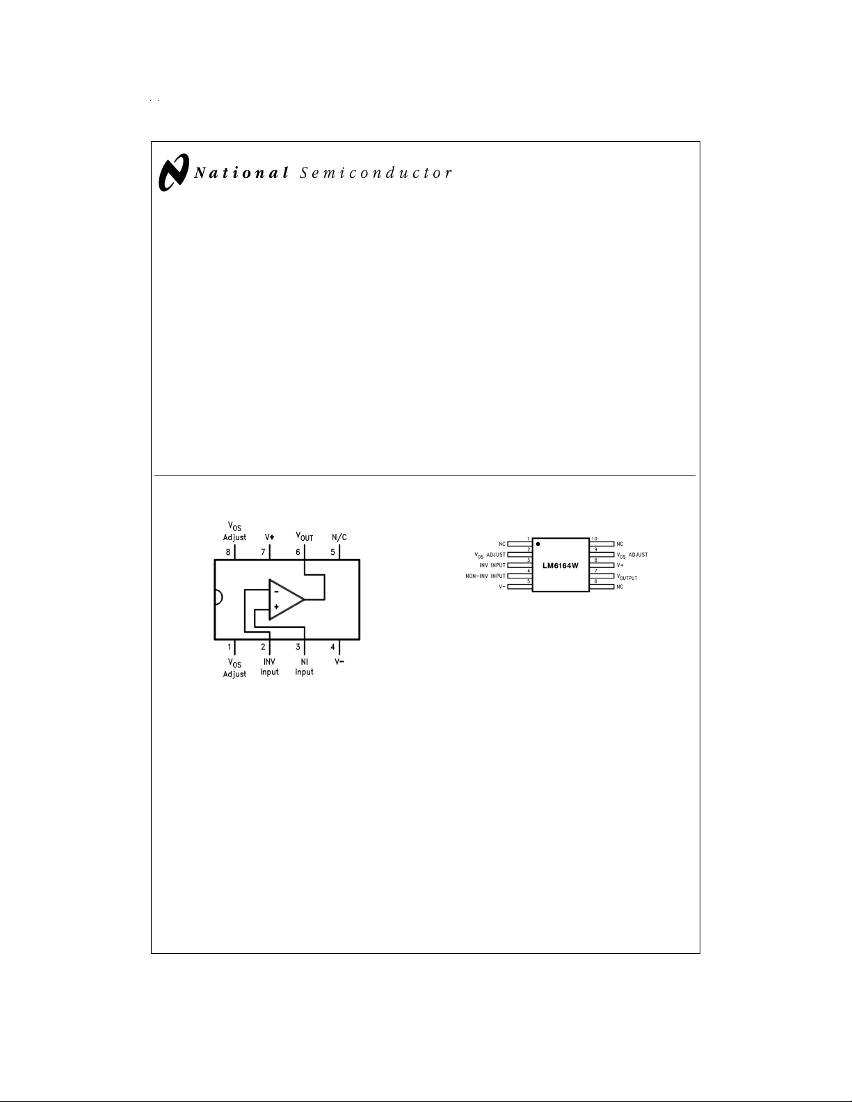
Connection Diagrams
Features
n High slew rate: 300 V/µs
n High GBW product: 175 MHz
n Low supply current: 5 mA
n Fast settling: 100 ns to 0.1
n Low differential gain:
n Low differential phase:
n Wide supply range: 4.75V to 32V
n Stable with unlimited capacitive load
%
<
%
0.1
<
0.1˚
Applications
n Video amplifier
n Wide-bandwidth signal conditioning
n Radar
n Sonar
10-Lead Flatpak
NS Package Number W10A
Top View
DS009153-15
DS009153-8
NS Package Number
J08A, M08A or N08E
VIP™is a trademark of National Semiconductor Corporation.
© 1999 National Semiconductor Corporation DS009153 www.national.com

Connection Diagrams (Continued)
Temperature Range Package NSC
Military Industrial Commercial
−55˚C ≤ T
LM6164J/883 8-Pin Ceramic DIP J08A
5962-8962401PA
LM6164WG/883 10-Lead Ceramic SOIC WG10A
5962-8962401XA
LM6164W/883 10-Pin W10A
5962-8962401HA Ceramic Flatpak
≤ +125˚C −25˚C ≤ TA≤ +85˚C 0˚C ≤ TA≤ +70˚C
A
LM6264N LM6364N 8-Pin Molded DIP N08E
LM6364M 8-Pin Molded Surface Mt. M08A
Drawing
www.national.com 2

Absolute Maximum Ratings (Note 1)
If Military/Aerospace specified devices are required,
please contact the National Semiconductor Sales Office/
Distributors for availability and specifications.
Supply Voltage (V
Differential Input Voltage
(Note 7)
Common-Mode Input Voltage
(Note 11) (V
Output Short Circuit to Gnd
(Note 2) Continuous
Soldering Information
Dual-In-Line Package (N, J)
Soldering (10 sec.) 260˚C
Small Outline Package (M)
Vapor Phase (60 sec.) 215˚C
Infrared (15 sec.) 220˚C
+−V−
) 36V
+
− 0.7V) to (V−+ 0.7V)
±
See AN-450 “Surface Mounting Methods and Their Effect
on Product Reliability” for other methods of soldering
surface mount devices.
Storage Temperature Range −65˚C to +150˚C
Max Junction Temperature
(Note 3) 150˚C
ESD Tolerance (Notes 7, 8)
8V
Operating Ratings
Temperature Range (Note 3)
LM6164 −55˚C ≤ T
LM6264 −25˚C ≤ T
LM6364 0˚C ≤ T
Supply Voltage Range 4.75V to 32V
Note 1: “Absolute Maximum Ratings” indicate limits beyond which damage
to the device may occur. Operating Ratings indicate conditions for which the
device is functional, but do not guarantee specific performance limits.
±
≤ +125˚C
J
≤ +85˚C
J
≤ +70˚C
J
700V
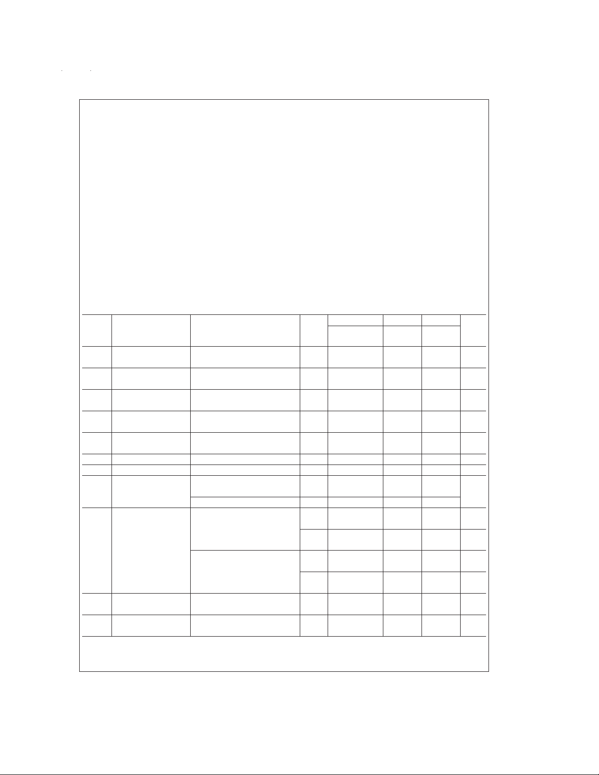
DC Electrical Characteristics
=
The following specifications apply for Supply Voltage
Boldface limits apply for T
=
=
T
A
to T
T
J
MIN
MAX
±
15V, V
; all other limits T
Symbol Parameter Conditions Typ Limit Limit Limit Units
V
V
Input Offset Voltage 2 4 4 9 mV
OS
Input Offset Voltage 6 µV/˚C
OS
Drift Average Drift
I
b
I
OS
I
OS
Input Bias Current 2.5 3 3 5 µA
Input Offset Current 150 350 350 1500 nA
Input Offset Current 0.3 nA/˚C
Drift Average Drift
R
C
A
Input Resistance Differential 100 kΩ
IN
Input Capacitance 3.0 pF
IN
Large Signal V
VOL
OUT
=
±
10V, R
=
2kΩ 2.5 1.8 1.8 1.3 V/mV
L
Voltage Gain (Note 10) 0.9 1.2 1.1 min
=
R
10 kΩ 9
L
=
V
Input Common-Mode Supply
CM
±
15V +14.0 +13.9 +13.9 +13.8 V
Voltage Range +13.8 +13.8 +13.7 min
Supply=+5V 4.0 3.9 3.9 3.8 V
(Note 5) 3.8 3.8 3.7 min
CMRR Common-Mode −10V ≤ V
≤ +10V 105 86 86 80 dB
CM
Rejection Ratio 80 82 78 min
PSRR Power Supply
±
10V ≤ V±≤±16V 96 86 86 80 dB
Rejection Ratio 80 82 78 min
=
≥ 100 kΩ and R
0, R
CM
L
=
=
T
25˚C.
A
J
=
50Ω unless otherwise noted.
S
LM6164 LM6264 LM6364
(Notes 4, 12) (Note 4) (Note 4)
6611max
656max
800 600 1900 max
−13.5 −13.3 −13.3 −13.2 V
−13.1 −13.1 −13.1 min
1.5 1.7 1.7 1.8 V
1.9 1.9 1.9 max
www.national.com3

DC Electrical Characteristics (Continued)
=
The following specifications apply for Supply Voltage
Boldface limits apply for T
=
=
T
A
to T
T
J
MIN
MAX
±
15V, V
; all other limits T
Symbol Parameter Conditions Typ Limit Limit Limit Units
V
Output Voltage Supply=+5V +14.2 +13.5 +13.5 +13.4 V
O
Swing and R
=
2kΩ +13.3 +13.3 +13.3 min
L
Supply=+5V 4.2 3.5 3.5 3.4 V
=
and R
2kΩ 3.3 3.3 3.3 min
L
(Note 10) 1.3 1.7 1.7 1.8 V
Output Short Source 65 30 30 30 mA
Circuit Current 20 25 25 min
Sink 65 30 30 30 mA
I
S
Supply Current 5.0 6.5 6.5 6.8 mA
=
≥ 100 kΩ and R
0, R
CM
L
=
=
T
25˚C.
A
J
=
50Ω unless otherwise noted.
S
LM6164 LM6264 LM6364
(Notes 4, 12) (Note 4) (Note 4)
−13.4 −13.0 −13.0 −12.9 V
−12.7 −12.8 −12.8 min
2.0 1.9 1.9 max
20 25 25 min
6.8 6.7 6.9 min
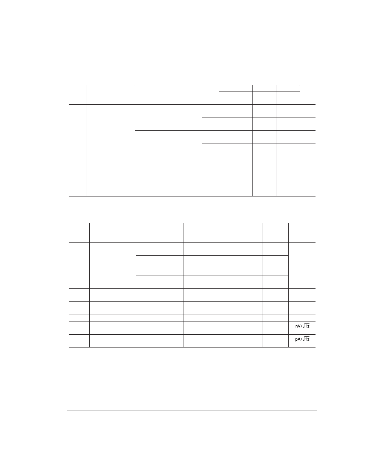
AC Electrical Characteristics
=
The following specifications apply for Supply Voltage
Boldface limits apply for T
=
=
T
A
to T
T
J
MIN
MAX
±
15V, V
; all other limits T
Symbol Parameter Conditions Typ Limit Limit Limit Units
GBW Gain-Bandwidth F=20 MHz 175 140 140 120 MHz
Product 100 120 100
=
±
5V 120
=
+5 (Note 9) 300 200 200 200 V/µs
=
±
5V 200
=
20 V
PP
%
=
=
=
−4, R
2kΩ
L
+5 45 Deg
=
+10
V
=
+10
V
SR Slew Rate A
PBW Power Bandwidth V
T
S
φ
m
A
D
φ
D
e
np-p
Settling Time 10V Step to 0.1
Phase Margin A
Differential Gain NTSC, A
Differential Phase NTSC, A
Input Noise F=10 kHz 8
Supply
V
Supply
OUT
A
V
V
Voltage
i
np-p
Input Noise F=10 kHz 1.5
Current
Note 2: Continuous short-circuit operation at elevated ambient temperature can result in exceeding the maximum allowed junction temperature of 150˚C.
Note 3: The typical junction-to-ambient thermal resistance of the molded plastic DIP (N) is 105˚C/Watt, the molded plastic SO (M) package is 155˚C/Watt, and the
cerdip (J) package is 125˚C/Watt. All numbers apply for packages soldered directly into a printed circuit board.
Note 4: Limits are guaranteed by testing or correlation.
Note 5: For single supply operation, the following conditions apply: V
−
) to realize maximum output swing. This connection will degrade VOS.
Pin4(V
Note 6: C
≤ 5pF.
L
Note 7: Inorder to achieve optimum AC performance, the input stage was designed without protective clamps. Exceeding the maximum differential input voltage results in reverse breakdown of the base-emitter junction of one of the input transistors and probable degradation of the input parameters (especially V
Noise).
Note 8: Theaveragevoltagethattheweakestpincombinations(thoseinvolvingPin2orPin 3) can withstand and still conform to the datasheet limits. The test circuit
used consists of the human body model of 100 pF in series with 1500Ω.
+
=
5V,V
=
≥ 100 kΩ and R
0, R
CM
L
=
=
T
A
25˚C.
J
=
50Ω unless otherwise noted.
S
LM6164 LM6264 LM6364
(Notes 4, 12) (Note 4) (Note 4)
180 180 180
4.5 MHz
100 ns
<
0.1
<
0.1 Deg
−
=
0V,V
=
CM
2.5V,V
=
2.5V.Pin1&Pin8(V
OUT
Adjust) are each connected to
OS
OS,IOS
min
min
%
, and
www.national.com 4
 Loading...