

NSC LM6182IN, LM6182IMX, LM6182IM, LM6182AIN Datasheet
LM6182
Dual 100 mA Output, 100 MHz Current Feedback
Amplifier
General Description
The LM6182 dual current feedback amplifier offers an unparalleled combination of bandwidth, slew-rate, and output current. Each amplifier can directly drive a 2V signal into a 50Ω
or 75Ω back-terminated coax cable system over the full industrial temperature range. This represents a radical enhancement in output drive capability for a dual 8-pin
high-speed amplifier making it ideal for video applications.
Built on National’s advanced high-speed VIP II
™
(Vertically
Integrated PNP) process, the LM6182 employs
current-feedback providing bandwidth that does not vary
dramatically with gain; 100 MHz at Av=−1, 60 MHz at Av
=
−10. With a slew rate of 2000 V/µsec, 2nd harmonic distortion of −50 dBc at 10 MHz and settling time of 50 ns (0.1%),
the two independent amplifiers of the LM6182 offer performance that is ideal for data acquisition, high-speed ATE,and
precision pulse amplifier applications.
See the LM6181 data sheet for a single amplifier with these
same features.
Features
(Typical unless otherwise noted)
n Slew Rate: 2000 V/µs
n Closed Loop Bandwidth: 100 MHz
n Settling Time (0.1%): 50 ns
n Low Differential Gain and Phase Error: 0.05%, 0.04˚
R
L
=
150Ω
n Low Offset Voltage: 2 mV
n High Output Drive:
±
10V into 150Ω
n Characterized for Supply Ranges:
±
5V and±15V
n Improved Performance over OP260 and LT1229
Applications
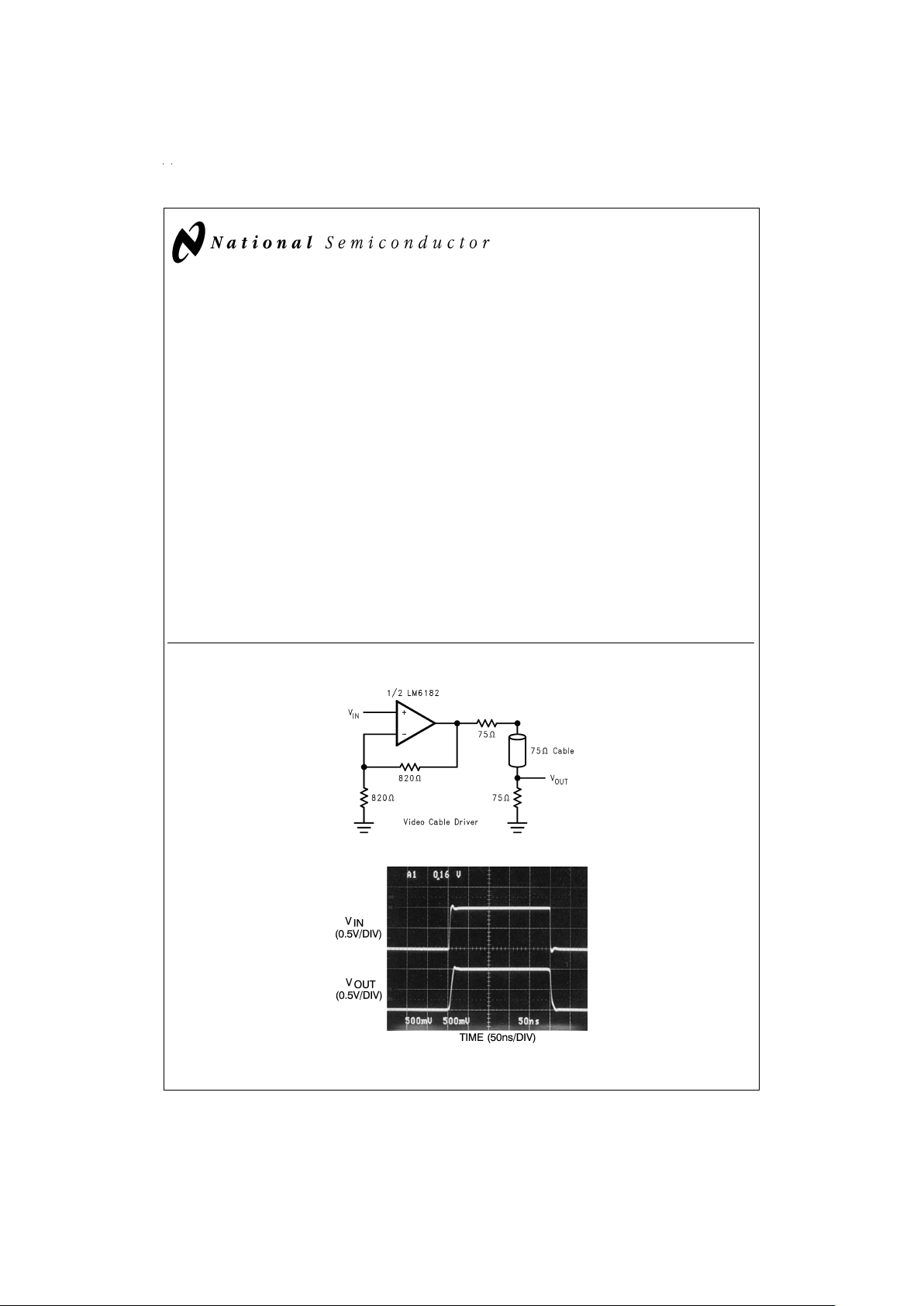
n Coax Cable Driver
n Professional Studio Video Equipment
n Flash ADC Buffer
n PC and Workstation Video Boards
n Facsimile and Imaging Systems
Typical Application
VIP II™is a trademark ofNational Semiconductor Corporation.
DS011926-1
DS011926-2
April 1994
LM6182 Dual 100 mA Output, 100 MHz Current Feedback Amplifier
© 1999 National Semiconductor Corporation DS011926 www.national.com
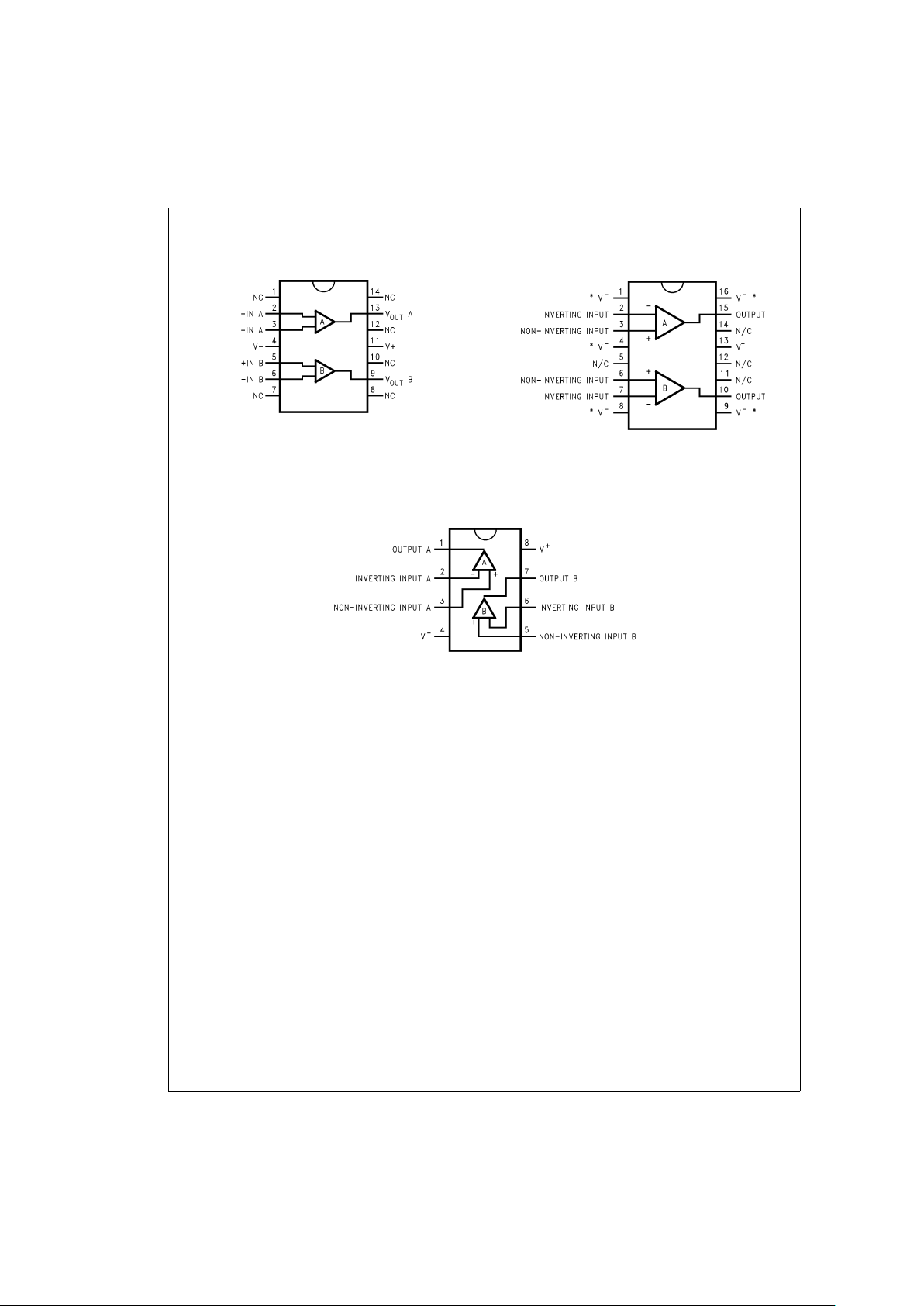
Connection Diagrams
Dual-In-Line Package (J)
DS011926-51
Order Number LM6182AMJ/883
See NS Package Number J14A
Small Outline Package (M)
DS011926-4
*
Heat Sinking Pins (Note 3)
Order Number LM6182IM or LM6182AIM
See NS Package Number M16A
Dual-In-Line Package (N)
DS011926-3
Order Number LM6182IN, LM6182AIN or LM6182AMN
See NS Package Number N08E
www.national.com 2
Absolute Maximum Ratings (Note 1)
If Military/Aerospace specified devices are required,
please contact the National Semiconductor Sales Office/
Distributors for availability and specifications.
Supply Voltage
±
18V
Differential Input Voltage
±
6V
Input Voltage
±
Supply Voltage
Inverting Input Current 15 mA
Output Short Circuit (Note 4)
Soldering Information
Dual-In-Line Package (N)
Soldering (10s) 260˚C
Small Outline Package (M)
Vapor Phase (60s) 215˚C
Infrared (15s) 220˚C
Storage Temperature Range −65˚C ≤ T
J
≤ +150˚C
Junction Temperature 150˚C
ESD Rating (Note 2)
±
2000V
Operating Ratings
Supply Voltage Range 7V to 32V
Junction Temperature Range (Note 3)
LM6182AM −55˚C ≤ T
J
≤ +125˚C
LM6182AI, LM6182I −40˚C ≤ T
J
≤ +85˚C
±
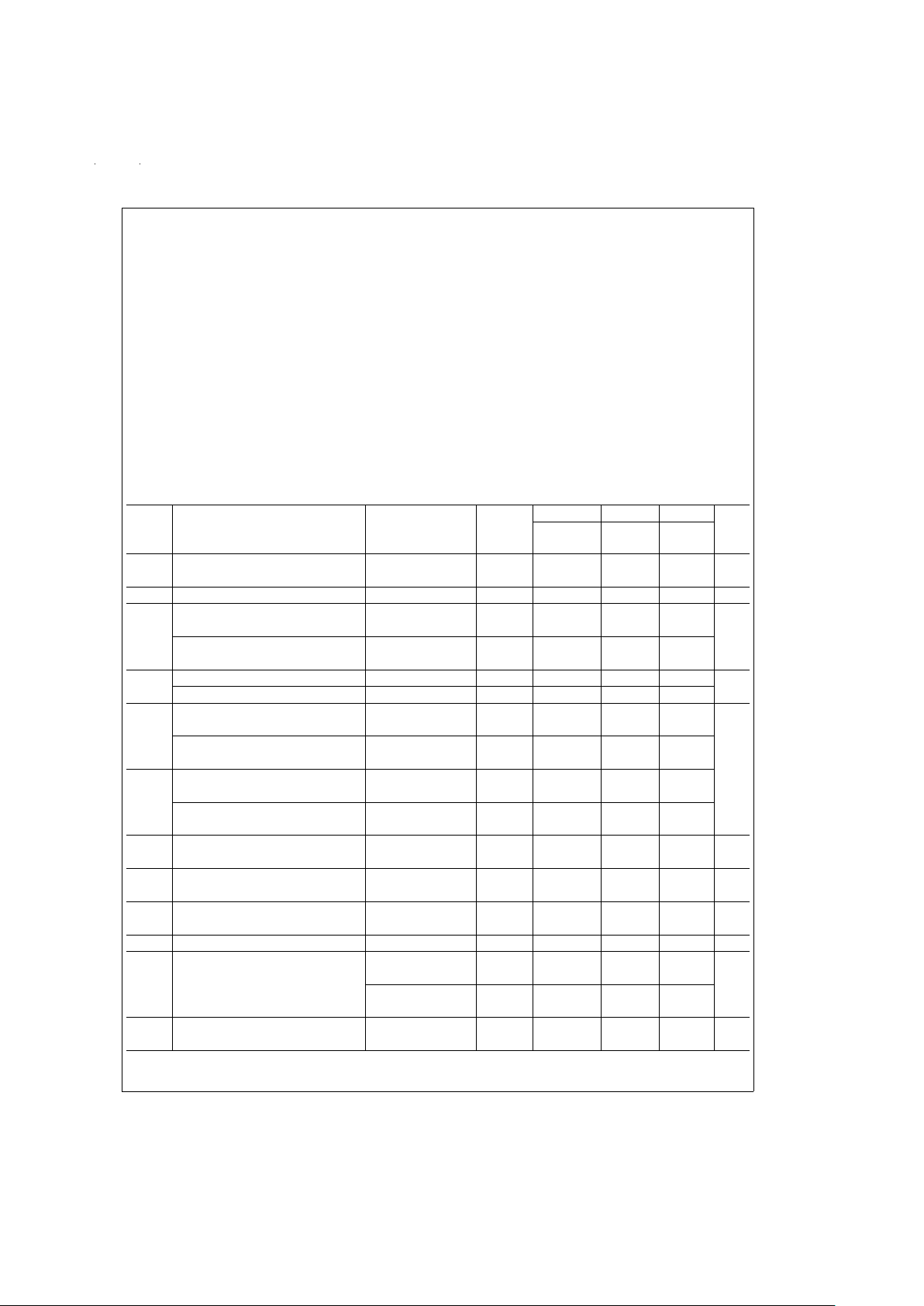
15V DC Electrical Characteristics
The following specifications apply for supply voltage
=
±
15V, Vcm=V
O
=
0V, R
f
=
820Ω, and R
L
=
1kΩunless otherwise
noted. Boldface limits apply at the temperature extremes; all other limits T
J
=
25˚C.
Symbol Parameter Conditions Typical
(Note 5)
LM6182AM LM6182AI LM6182I Units
Limit Limit Limit
(Note 6) (Note 6) (Note 6)
V
OS
Input Offset Voltage 2.0 3.0 3.0 5.0 mV
4.0 3.5 5.5 max
TCV
OS
Input Offset Voltage Drift 5.0 µV/˚C
I
B
Inverting Input Bias Current 2.0 5.0 5.0 10.0 µA
max
12.0 12.0 17.0
Non-Inverting Input Bias Current 0.75 2.0 2.0 3.0
4.0 4.0 5.0
TCI
B
Inverting Input Bias Current Drift 30 nA/˚C
Non-Inverting Input Bias Current Drift 10
I
B
Inverting Input Bias Current
±
4.5V ≤ VS≤±16V 0.1 0.5 0.5 0.75 µA/V
max
PSR Power Supply Rejection 3.0 3.0 4.5
Non-Inverting Input Bias Current
±
4.5V ≤ VS≤±16V 0.05 0.5 0.5 0.5
Power Supply Rejection 1.5 1.5 3.0
I
B
Inverting Input Bias Current −10V ≤ VCM≤ +10V 0.15 0.5 0.5 0.75
CMR Common Mode Rejection 1.0 1.0 1.5
Non-Inverting Input Bias Current −10V ≤ V
CM
≤ +10V 0.1 0.5 0.5 0.5
Common Mode Rejection 1.0 1.0 1.5
CMRR Common Mode Rejection Ratio −10V ≤ V
CM
≤ +10V 60 50 50 50 dB
47 47 47 min
PSRR Power Supply Rejection Ratio
±
4.5V ≤ VS≤±16V 80 70 70 70 dB
67 67 65 min
R
O
Output Resistance A
V
=
−1 0.2 Ω
f=300 kHz
R
IN
Non-Inverting Input Resistance 10 MΩ
V
O
Output Voltage Swing R
L
=
1kΩ 12 11 11 11 V
min
10 10 10
R
L
=
150Ω 11 9.5 9.5 9.5
5.6 6.0 6.0
I
SC
Output Short Circuit Current 100 70 70 70 mA
37.5 40 40 min
www.national.com3
±
15V DC Electrical Characteristics (Continued)
The following specifications apply for supply voltage
=
±
15V, Vcm=V
O
=
0V, R
f
=
820Ω, and R
L
=
1kΩunless otherwise
noted. Boldface limits apply at the temperature extremes; all other limits T
J
=
25˚C.
Symbol Parameter Conditions Typical
(Note 5)
LM6182AM LM6182AI LM6182I Units
Limit Limit Limit
(Note 6) (Note 6) (Note 6)
Z
T
Transimpedance R
L
=
1kΩ 1.8 1.0 1.0 0.8 MΩ
min
0.4 0.5 0.4
R
L
=
150Ω 1.4 0.8 0.8 0.7
0.3 0.35 0.3
I
S
Supply Current No Load, V
IN
=
0V 15 20 20 20 mA
Both Amplifiers 22 22 22 max
V
CM
Input Common Mode Voltage Range V+−1.7V V
V
−
+1.7V
±
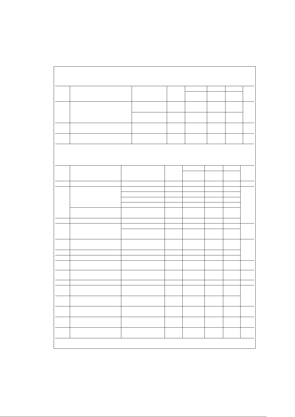
15V AC Electrical Characteristics
The following specifications apply for supply voltage
=
±
15V, Vcm=V
O
=
0V, R
f
=
820Ω, and R
L
=
1kΩunless otherwise
noted. Boldface limits apply at the temperature extremes; all other limits T
J
=
25˚C.
Symbol Parameter Conditions Typical
(Note 5)
LM6182AM LM6182AI LM6182I Units
Limit Limit Limit
(Note 6) (Note 6) (Note 6)
Xt Crosstalk Rejection (Note 7) 93 dB
BW Closed Loop Bandwidth −3 dB A
V
=
+2 100 MHz
A
V
=
+10 75
A
V
=
−1 100
A
V
=
−10 60
Closed Loop Bandwidth A
V
=
+2, R
L
=
150Ω 35
0.1 dB Flat, R
SOURCE
=
200Ω
PBW Power Bandwidth A
V
=
−1, V
O
=
5V
PP
60
SR Slew Rate Overdriven 2000 V/µs
min
A
V
=
−1, V
O
=
±
10V 1400 1000 1000 1000
R
L
=
150Ω, (Note 8)
t
s
Settling Time (0.1%)A
V
=
−1, V
O
=
±
5V 50 ns
R
L
=
150Ω
t
r,tf
Rise and Fall Time V
O
=
1V
PP
5
t
p
Propagation Delay Time V
O
=
1V
PP
6
in(+) Non-Inverting Input Noise
Current Density
f=1 kHz 3 pA/
√
Hz
in(−) Inverting Input Noise
Current Density
f=1 kHz 16 pA/
√
Hz
e
n
Input Noise Voltage Density f=1 kHz 4 nV/√Hz
Second Harmonic Distortion V
O
=
2V
PP
,f=10 MHz -50 dBc
A
V
=
+2
Third Harmonic Distortion V
O
=
2V
PP
,f=10 MHz -55
A
V
=
+2
Differential Gain R
L
=
150Ω 0.05
%
A
V
=
+2, NTSC
Differential Phase R
L
=
150Ω 0.04 Deg
A
V
=
+2, NTSC
THD Total Harmonic Distortion V
O
=
2V
PP,AV
=
+2, 0.58
%
f=10 MHz, R
L
=
150Ω
www.national.com 4
±
5V DC Electrical Characteristics
The following specifications apply for supply voltage
=
±
5V, Vcm=V
O
=
0V, R
f
=
820Ω, and R
L
=
1kΩunless otherwise
noted. Boldface limits apply at the temperature extremes; all other limits T
J
=
25˚C.
Symbol Parameter Conditions Typical
(Note 5)
LM6182AM LM6182AI LM6182I Units
Limit Limit Limit
(Note 6) (Note 6) (Note 6)
V
OS
Input Offset Voltage 1.0 2.0 2.0 3.0 mV
3.0 2.5 3.5 max
TCV
OS
Input Offset Voltage Drift 2.5 µV/˚C
I
B
Inverting Input Bias Current 5.0 10 10 17.5 µA
max
22 22 27.0
Non-Inverting Input Bias Current 0.25 1.5 1.5 3.0
3.0 3.0 5.0
TCI
B
Inverting Input Bias Current Drift 50 nA/˚C
Non-Inverting Input Bias Current Drift 3.0
I
B
Inverting Input Bias Current
±
4V ≤ VS≤±6V 0.3 0.5 0.5 0.75 µA/V
max
PSR Power Supply Rejection 1.0 1.0 1.5
Non-Inverting Input Bias Current
±
4V ≤ VS≤±6V 0.05 0.5 0.5 0.5
Power Supply Rejection 1.0 1.0 1.5
I
B
Inverting Input Bias Current −2.5V ≤ VCM≤ +2.5V 0.3 0.5 0.5 1.0
CMR Common Mode Rejection 1.0 1.0 1.5
Non-Inverting Input Bias Current −2.5V ≤ V
CM
≤ +2.5V 0.12 0.5 0.5 0.5
Common Mode Rejection 1.0 1.0 1.5
CMRR Common Mode Rejection Ratio −2.5V ≤ V
CM
≤ +2.5V 57 50 50 50 dB
min
47 47 47
PSRR Power Supply Rejection Ratio
±
4V ≤ VS≤±6V 80 70 70 64
67 67 60
R
O
Output Resistance A
V
=
−1 0.25 Ω
f=300 kHz
R
IN
Non-Inverting Input Resistance 8 MΩ
V
O
Output Voltage Swing R
L
=
1kΩ 2.6 2.25 2.25 2.25 V
min
2.0 2.0 2.0
R
L
=
150Ω 2.2 2.0 2.0 2.0
1.8 1.8 1.8
I
SC
Output Short Circuit Current 100 65 65 65 mA
35 40 40 min
Z
T
Transimpedance R
L
=
1kΩ 1.4 0.75 0.75 0.6 MΩ
min
0.3 0.35 0.3
R
L
=
150Ω 1.0 0.5 0.5 0.4
0.2 0.25 0.2
I
S
Supply Current No Load, V
IN
=
0V 13 17 17 17 mA
Both Amplifiers 18.5 18.5 18.5 max
V
CM
Input Common Mode Voltage Range V+−1.7V V
V
−
+1.7V
www.national.com5
±
5V AC Electrical Characteristics
The following specifications apply for supply voltage
=
±
5V, Vcm=V
O
=
0V, R
f
=
820Ω, and R
L
=
1kΩunless otherwise
noted. Boldface limits apply at the temperature extremes; all other limits T
J
=
25˚C.
Symbol Parameter Conditions Typical
(Note 5)
LM6182AM LM6182AI LM6182I Units
Limit Limit Limit
(Note 6) (Note 6) (Note 6)
Xt Crosstalk Rejection (Note 7) 92 dB
BW Closed Loop Bandwidth −3 dB A
V
=
+2 50 MHz
A
V
=
+10 40
A
V
=
−1 55
A
V
=
−10 35
Closed Loop Bandwidth A
V
=
+2, R
L
=
150Ω 15
0.1 dB Flat, R
SOURCE
=
200Ω
PBW Power Bandwidth A
V
=
−1, V
O
=
4V
PP
40
SR Slew Rate A
V
=
−1, V
O
=
±
2V 500 375 375 375 V/µs
R
L
=
150Ω, (Note 8) min
t
s
Settling Time (0.1%)A
V
=
−1, V
O
=
±
2V 50 ns
R
L
=
150Ω
t
r,tf
Rise and Fall Time V
O
=
1V
PP
8.5
t
p
Propagation Delay Time V
O
=
1V
PP
8
in(+) Non-Inverting Input Noise
Current Density
f=1 kHz 3 pA/
√
Hz
in(−) Inverting Input Noise
Current Density
f=1 kHz 16 pA/
√
Hz
e
n
Input Noise Voltage Density f=1 kHz 4 nV/√Hz
Second Harmonic Distortion V
O
=
2V
PP
,f=10 MHz -45 dBc
A
V
=
+2
Third Harmonic Distortion V
O
=
2V
PP
,f=10 MHz -55
A
V
=
+2
Differential Gain R
L
=
150Ω 0.06
%
A
V
=
+2, NTSC
Differential Phase R
L
=
150Ω 0.16 Deg
A
V
=
+2, NTSC
THD Total Harmonic Distortion V
O
=
2V
PP,AV
=
+2, 0.36
%
f=5 MHz, R
L
=
150Ω
Note 1: Absolute Maximum Ratings indicate limits beyond which damage to the device may occur. Operating ratings indicate conditions for which the device is intended to be functional, but device parameter specifications may not be guaranteed under these conditions. For guaranteed specifications and test conditions, see
the Electrical Characteristics.
Note 2: Human body model 100 pF and 1.5 kΩ.
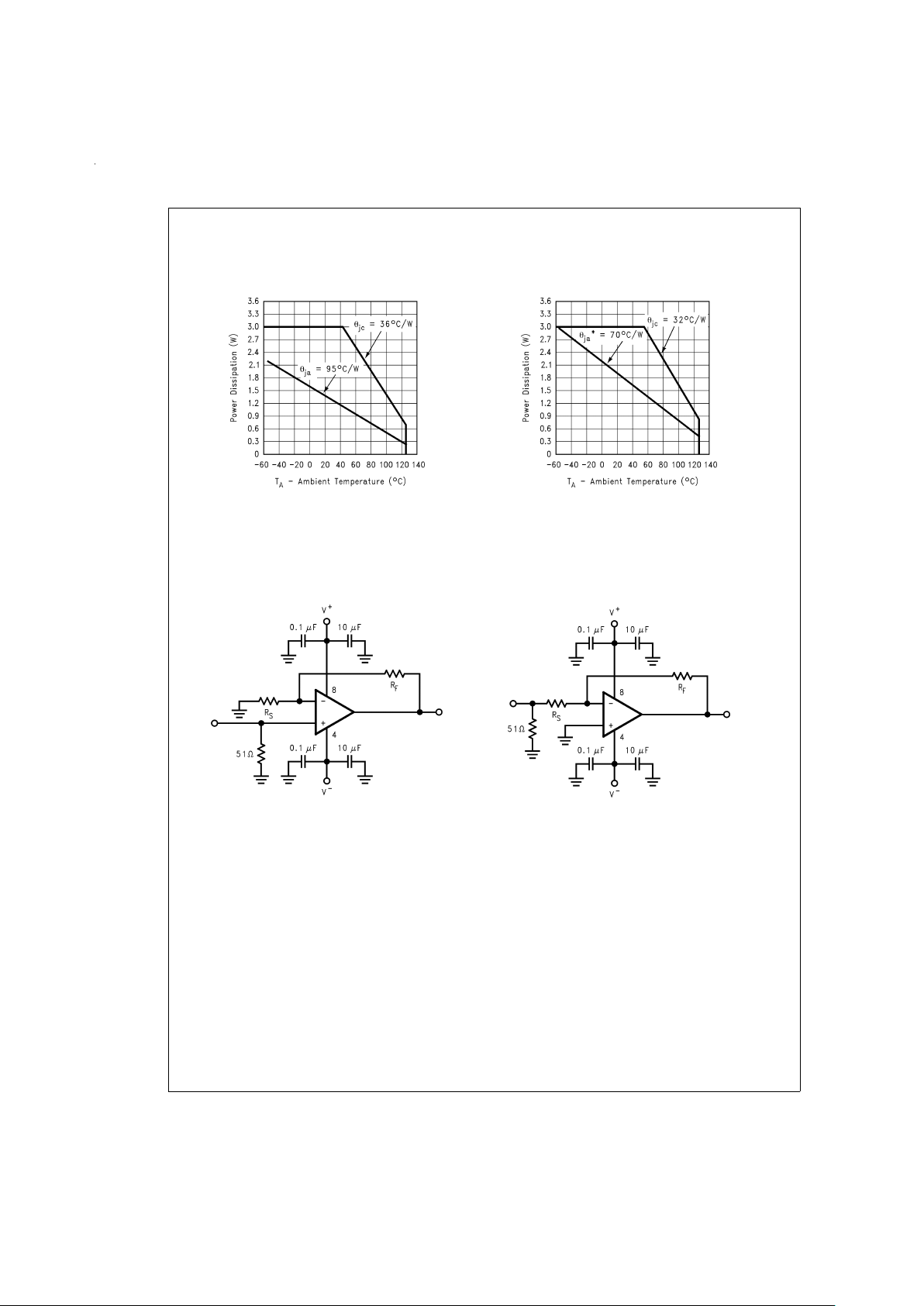
Note 3: The typical junction-to-ambient thermal resistance of the molded plastic DIP(N) soldered directly into a PC board is 95˚C/W. The junction-to-ambient thermal
resistance of the S.O. surface mount (M) package mounted flush to the PC board is 70˚C/W when pins 1,4,8,9 and 16 are soldered to a total of 2 in
2
1 oz copper
trace. The S.O. (M) package must have pin 4 and at least one of pins 1,8,9, or 16 connected to V− for proper operation.
Note 4: Continuous short circuit operation at elevated ambient temperature can result in exceeding the maximum allowable junction temperature of 150˚C. Each am-
plifier of the LM6182 is short circuit current limited to 100 mA typical.
Note 5: Typical values represent the most likely parametric norm.
Note 6: All limits are guaranteed at room temperature (standard type face) or at operating temperature extremes (boldface type).
Note 7: Each amp excited in turn with 100 kHz to produce Vo=2 Vpp. Results are input referred.
Note 8: Measured from +25%to +75%of output waveform.
Note 9: Also available per the Standard Military Drawing, 5962-9460301MCA.
Note 10: For guaranteed military specifications see military datasheet MNLM6182AM-X.
www.national.com 6
±
5V AC Electrical Characteristics (Continued)
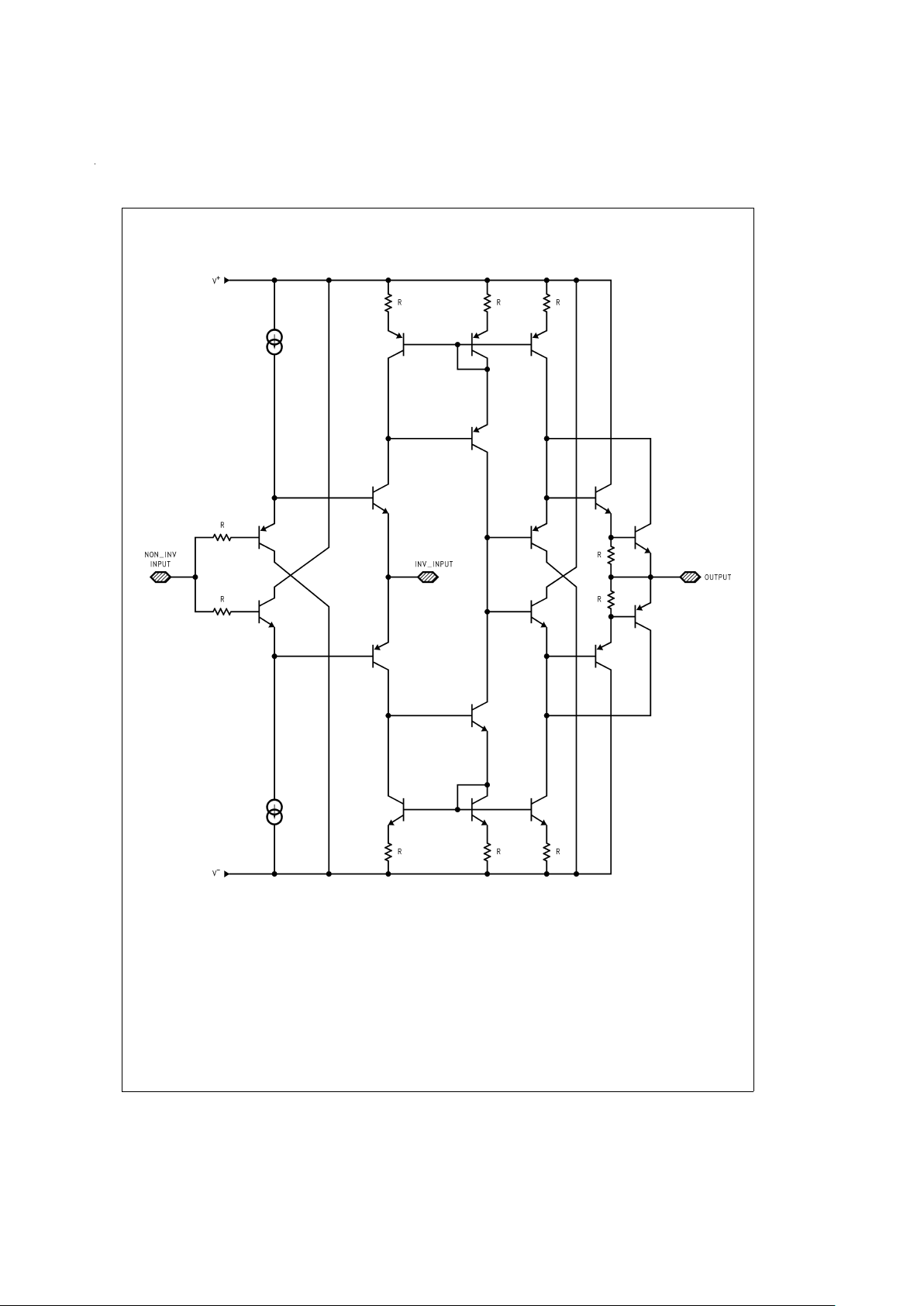
Simplified Schematic 1/2 LM6182
DS011926-6
www.national.com7
Typical Performance Characteristics
MAXIMUM POWER DERATING CURVES
TYPICAL PERFORMANCE TEST CIRCUITS
N-Package
DS011926-7
M-Package
DS011926-8
*
θ
ja
=
Thermal Resistance with 2 square inches of 1 ounce copper tied to
pins 1, 8, 9 and 16
Non-Inverting:
Small Signal Pulse Response,
Slew Rate, −3 dB Bandwidth
DS011926-9
Inverting:
Small Signal Pulse Response,
Slew Rate, −3 dB Bandwidth
DS011926-10
www.national.com 8
 Loading...