

NSC LM6181IN, LM6181IMX-8, LM6181IMX, LM6181IM, LM6181IM-8 Datasheet
LM6181
100 mA, 100 MHz Current Feedback Amplifier
General Description
The LM6181 current-feedback amplifier offers an unparalleled combination of bandwidth, slew-rate, and output current. The amplifier can directly drive up to 100 pF capacitive
loads without oscillating and a 10V signal into a 50Ω or 75Ω
back-terminated coax cable system over the full industrial
temperature range. This represents a radical enhancement
in output drive capability for an 8-pin DIP high-speed amplifier making it ideal for video applications.
Built on National’s advanced high-speed VIP
™
II (Vertically
Integrated PNP) process, the LM6181 employs currentfeedback providing bandwidth that does not vary dramatically with gain; 100 MHz at A
V
=
−1, 60 MHz at A
V
=
−10.
With a slew rate of2000V/µs,2ndharmonic distortion of −50
dBc at 10 MHz and settling time of 50 ns (0.1%) the LM6181
dynamic performance makes it ideal for data acquisition,
high speed ATE, and precision pulse amplifier applications.
Features
(Typical unless otherwise noted)
n Slew rate: 2000 V/µs
n Settling time (0.1%): 50 ns
n Characterized for supply ranges:
±
5V and±15V
n Low differential gain and phase error: 0.05%, 0.04˚
n High output drive:
±
10V into 100Ω
n Guaranteed bandwidth and slew rate
n Improved performance over EL2020, OP160, AD844,
LT1223 and HA5004
Applications
n Coax cable driver
n Video amplifier
n Flash ADC buffer
n High frequency filter
n Scanner and Imaging systems
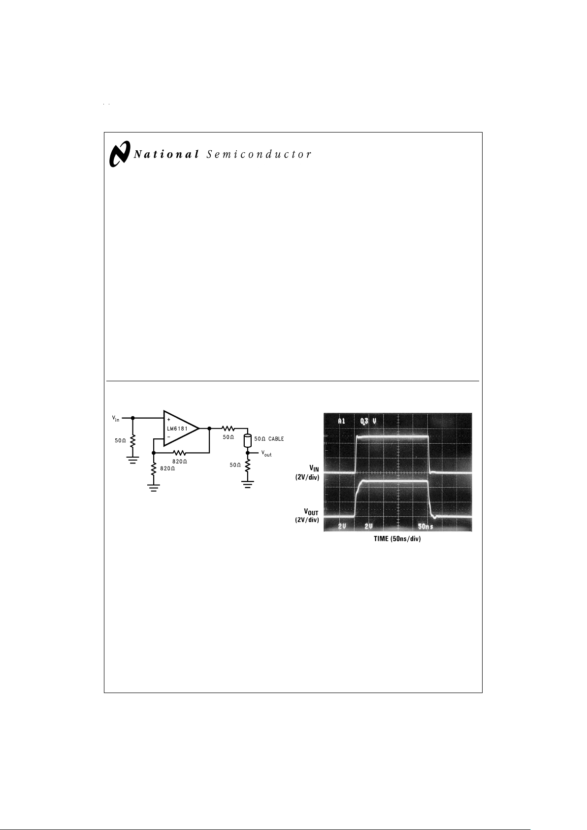
Typical Application
VIP™is a registered trademark of National Semiconductor Corporation.
DS011328-1
Cable Driver
DS011328-2
May 1998
LM6181 100 mA, 100 MHz Current Feedback Amplifier
© 1999 National Semiconductor Corporation DS011328 www.national.com
Absolute Maximum Ratings (Note 1)
If Military/Aerospace specified devices are required,
please contact the National Semiconductor Sales Office/
Distributors for availability and specifications.
Supply Voltage
±
18V
Differential Input Voltage
±
6V
Input Voltage
±
Supply Voltage
Inverting Input Current 15 mA
Soldering Information
Dual-In-Line Package (N)
Soldering (10 sec) 260˚C
Small Outline Package (M)
Vapor Phase (60 seconds) 215˚C
Infrared (15 seconds) 220˚C
Output Short Circuit (Note 7)
Storage Temperature Range −65˚C ≤ T
J
≤ +150˚C
Maximum Junction Temperature 150˚C
ESD Rating (Note 2)
±
3000V
Operating Ratings
Supply Voltage Range 7V to 32V
Junction Temperature Range (Note 3)
LM6181AM −55˚C ≤ T
J
≤ +125˚C
LM6181AI, LM6181I −40˚C ≤ T
J
≤ +85˚C
Thermal Resistance (θ
JA
, θJC)
8-pin DIP (N) 102˚C/W, 42˚C/W
8-pin SO (M-8) 153˚C/W, 42˚C/W
16-pin SO (M) 70˚C/W, 38˚C/W
±
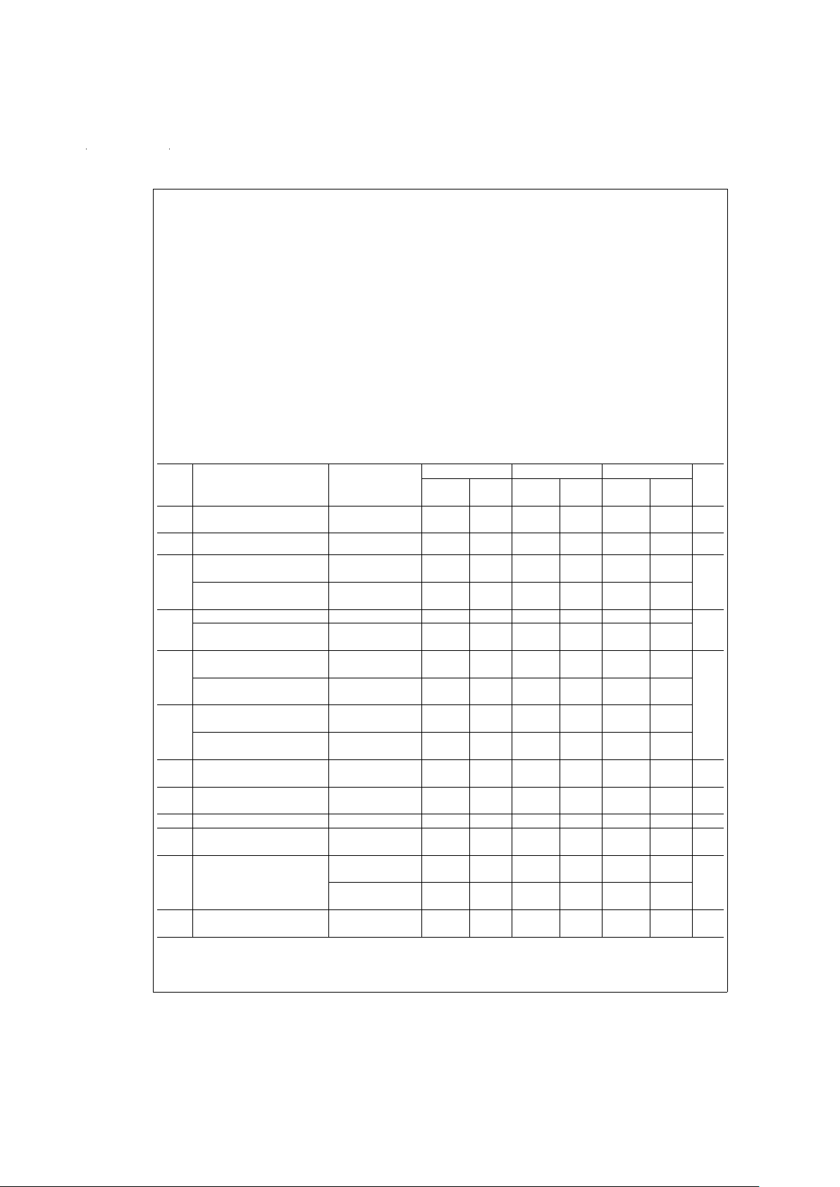
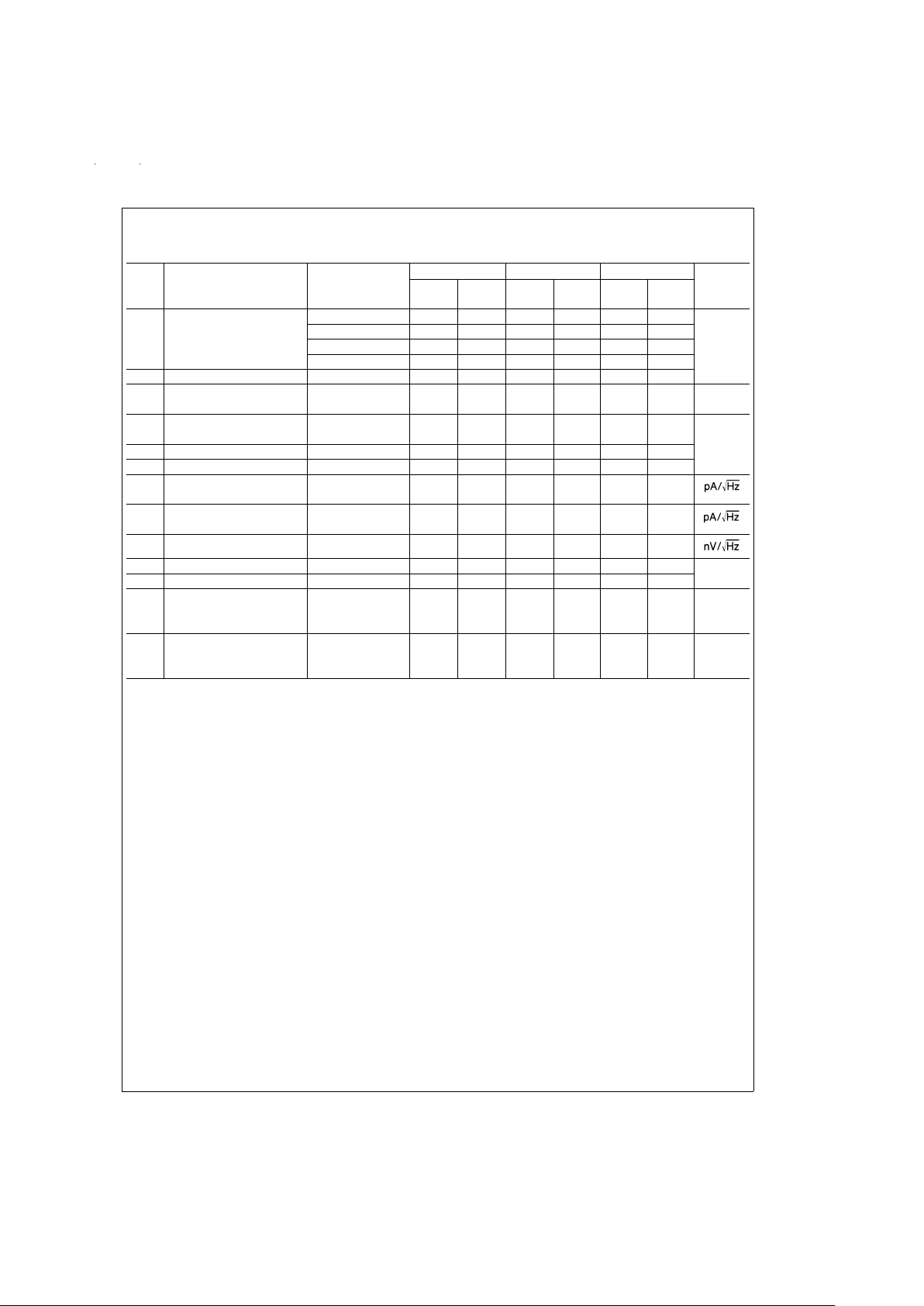
15V DC Electrical Characteristics
The following specifications apply for Supply Voltage
=
±
15V, R
F
=
820Ω, and R
L
=
1kΩunless otherwise noted. Boldface
limits apply at the temperature extremes; all other limits T
J
=
25˚C.
Symbol Parameter Conditions LM6181AM LM6181AI LM6181I Units
Typical Limit Typical Limit Typical Limit
(Note 4) (Note 5) (Note 4) (Note 5) (Note 4) (Note 5)
V
OS
Input Offset Voltage 2.0 3.0 2.0 3.0 3.5 5.0 mV
4.0 3.5 5.5 max
TC
V
OS
Input Offset Voltage Drift 5.0 5.0 5.0 µV/˚C
I
B
Inverting Input Bias Current 2.0 5.0 2.0 5.0 5.0 10 µA
max
12.0 12.0 17.0
Non-Inverting Input Bias Current 0.5 1.5 0.5 1.5 2.0 3.0
3.0 3.0 5.0
TC I
B
Inverting Input Bias Current Drift 30 30 30 nA/˚C
Non-Inverting Input Bias 10 10 10
Current Drift
I
B
Inverting Input Bias Current V
S
=
±
4.5V,±16V 0.3 0.5 0.3 0.5 0.3 0.75 µA/V
max
PSR Power Supply Rejection 3.0 3.0 4.5
Non-Inverting Input Bias Current V
S
=
±
4.5V,±16V 0.05 0.5 0.05 0.5 0.05 0.5
Power Supply Rejection 1.5 1.5 3.0
I
B
Inverting Input Bias Current −10V ≤ VCM≤ +10V 0.3 0.5 0.3 0.5 0.3 0.75
CMR Common Mode Rejection 0.75 0.75 1.0
Non-Inverting Input Bias Current −10V ≤ V
CM
≤ +10V 0.1 0.5 0.1 0.5 0.1 0.5
Common Mode Rejection 0.5 0.5 0.5
CMRR Common Mode Rejection Ratio −10V ≤ V
CM
≤ +10V 60 50 60 50 60 50 dB
50 50 50 min
PSRR Power Supply Rejection Ratio V
S
=
±
4.5V,±16V 80 70 80 70 80 70 dB
70 70 65 min
R
O
Output Resistance A
V
=
−1, f=300 kHz 0.2 0.2 0.2 Ω
R
IN
Non-Inverting Input Resistance 10 10 10 MΩ
min
V
O
Output Voltage Swing R
L
=
1kΩ 12 11 12 11 12 11 V
min
11 11 11
R
L
=
100Ω 11 10 11 10 11 10
7.5 8.0 8.0
I
SC
Output Short Circuit Current 130 100 130 100 130 100 mA
75 85 85 min
www.national.com 2
±
15V DC Electrical Characteristics (Continued)
The following specifications apply for Supply Voltage
=
±
15V, R
F
=
820Ω, and R
L
=
1kΩunless otherwise noted. Boldface
limits apply at the temperature extremes; all other limits T
J
=
25˚C.
Symbol Parameter Conditions LM6181AM LM6181AI LM6181I Units
Typical Limit Typical Limit Typical Limit
(Note 4) (Note 5) (Note 4) (Note 5) (Note 4) (Note 5)
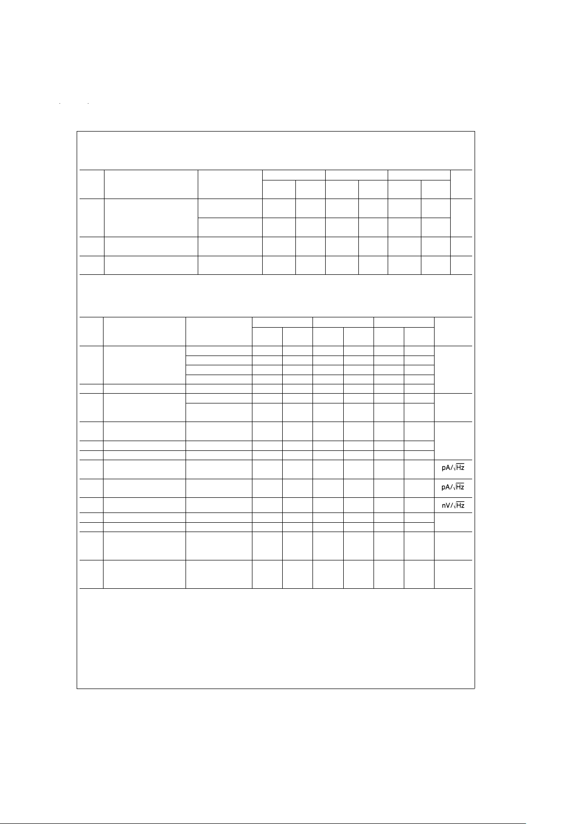
Z
T
Transimpedance R
L
=
1kΩ 1.8 1.0 1.8 1.0 1.8 0.8
0.5 0.5 0.4 MΩ
R
L
=
100Ω 1.4 0.8 1.4 0.8 1.4 0.7 min
0.4 0.4 0.35
I
S
Supply Current No Load, V
O
=
0V 7.5 10 7.5 10 7.5 10 mA
10 10 10 max
V
CM
Input Common Mode V+− 1.7V V+− 1.7V V+− 1.7V V
Voltage Range V
−
+ 1.7V V−+ 1.7V V−+ 1.7V
±
15V AC Electrical Characteristics
The following specifications apply for Supply Voltage
=
±
15V, R
F
=
820Ω,R
L
=
1kΩunless otherwise noted. Boldface limits
apply at the temperature extremes; all other limits T
J
=
25˚C.
Symbol Parameter Conditions LM6181AM LM6181AI LM6181I Units
Typical Limit Typical Limit Typical Limit
(Note 4) (Note 5) (Note 4) (Note 5) (Note 4) (Note 5)
BW Closed Loop Bandwidth A
V
=
+2 100 100 100 MHz
min
−3 dB A
V
=
+10 80 80 80
A
V
=
−1 100 80 100 80 100 80
A
V
=
−10 60 60 60
PBW Power Bandwidth A
V
=
−1, V
O
=
5V
PP
60 60 60
SR Slew Rate Overdriven 2000 2000 2000 V/µs
min
A
V
=
−1, V
O
=
±
10V, 1400 1000 1400 1000 1400 1000
R
L
=
150Ω (Note 6)
t
s
Settling Time (0.1%)A
V
=
−1, V
O
=
±
5V 50 50 50 ns
R
L
=
150Ω
t
r,tf
Rise and Fall Time V
O
=
1V
PP
555
t
p
Propagation Delay Time V
O
=
1V
PP
666
i
n(+)
Non-Inverting Input Noise f=1 kHz 3 3 3
Current Density
i
n(−)
Inverting Input Noise f=1 kHz 16 16 16
Current Density
e
n
Input Noise Voltage
Density
f=1 kHz 4 4 4
Second Harmonic Distortion 2 VPP, 10 MHz −50 −50 −50 dBc
Third Harmonic Distortion 2 V
PP
, 10 MHz −55 −55 −50
Differential Gain R
L
=
150Ω
A
V
=
+2 0.05 0.05 0.05
%
NTSC
Differential Phase R
L
=
150Ω
A
V
=
+2 0.04 0.04 0.04 Deg
NTSC
www.national.com3
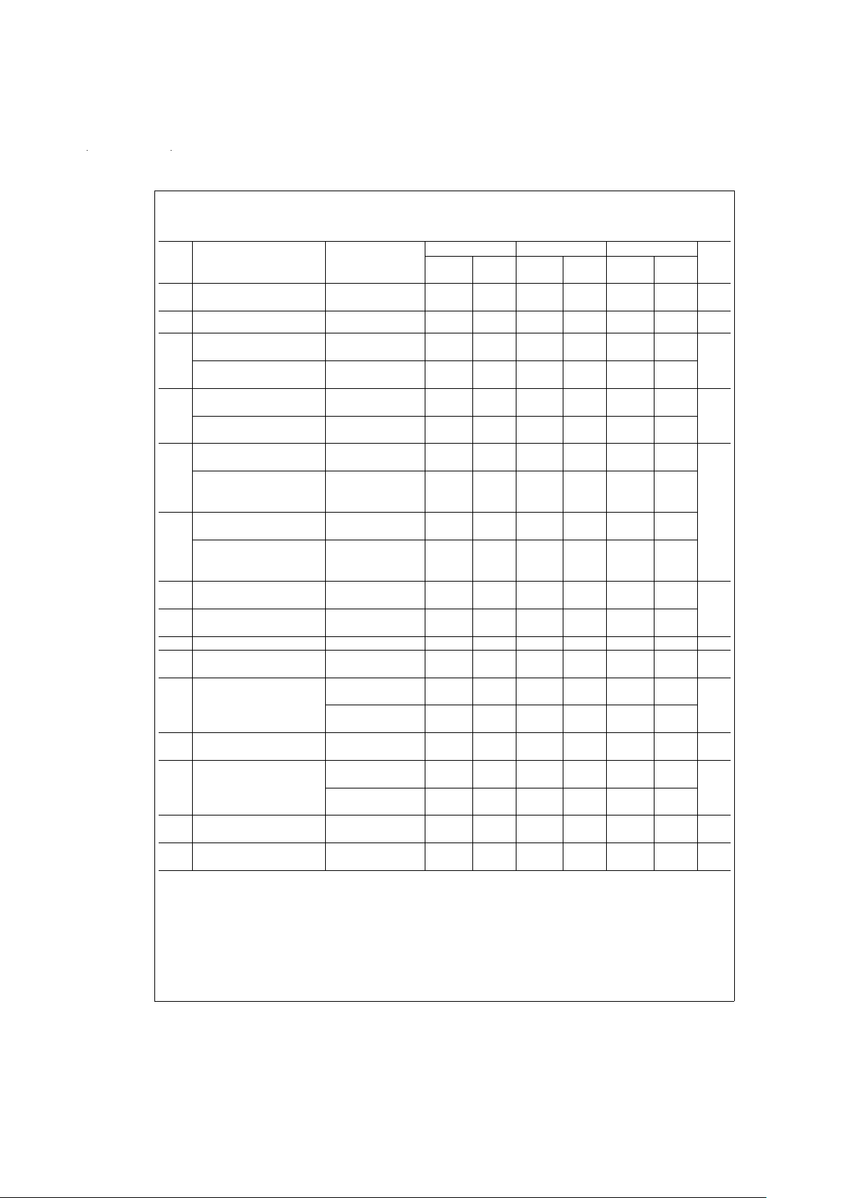
±
5V DC Electrical Characteristics
The following specifications apply for Supply Voltage
=
±
5V, R
F
=
820Ω, and R
L
=
1kΩunless otherwise noted. Boldface
limits apply at the temperature extremes; all other limits T
J
=
25˚C.
Symbol Parameter Conditions LM6181AM LM6181AI LM6181I Units
Typical Limit Typical Limit Typical Limit
(Note 4) (Note 5) (Note 4) (Note 5) (Note 4) (Note 5)
V
OS
Input Offset Voltage 1.0 2.0 1.0 2.0 1.0 3.0 mV
3.0 2.5 3.5 max
TC
V
OS
Input Offset Voltage Drift 2.5 2.5 2.5 µV/˚C
I
B
Inverting Input 5.0 10 5.0 10 5.0 17.5 µA
max
Bias Current 22 22 27.0
Non-Inverting Input 0.25 1.5 0.25 1.5 0.25 3.0
Bias Current 1.5 1.5 5.0
TC I
B
Inverting Input Bias 50 50 50 nA/˚C
Current Drift
Non-Inverting Input 3.0 3.0 3.0
Bias Current Drift
I
B
Inverting Input Bias Current V
S
=
±
4.0V,±6.0V 0.3 0.5 0.3 0.5 0.3 1.0 µA/V
max
PSR Power Supply Rejection 0.5 0.5 1.0
Non-Inverting Input V
S
=
±
4.0V,±6.0V 0.05 0.5 0.05 0.5 0.05 0.5
Bias Current
Power Supply Rejection 0.5 0.5 0.5
I
B
Inverting Input Bias Current −2.5V ≤ VCM≤ +2.5V 0.3 0.5 0.3 0.5 0.3 1.0
CMR Common Mode Rejection 1.0 1.0 1.5
Non-Inverting Input −2.5V ≤ V
CM
≤ +2.5V 0.12 0.5 0.12 0.5 0.12 0.5
Bias Current
Common Mode Rejection 1.0 0.5 0.5
CMRR Common Mode −2.5V ≤ V
CM
≤ +2.5V 57 50 57 50 57 50 dB
min
Rejection Ratio 47 47 47
PSRR Power Supply V
S
=
±
4.0V,±6.0V 80 70 80 70 80 64
Rejection Ratio 70 70 64
R
O
Output Resistance A
V
=
−1, f=300 kHz 0.25 0.25 0.25 Ω
R
IN
Non-Inverting 8 8 8 MΩ
Input Resistance min
V
O
Output Voltage Swing R
L
=
1kΩ 2.6 2.25 2.6 2.25 2.6 2.25 V
min
2.2 2.25 2.25
R
L
=
100Ω 2.2 2.0 2.2 2.0 2.2 2.0
2.0 2.0 2.0
I
SC
Output Short 100 75 100 75 100 75 mA
Circuit Current 70 70 70 min
Z
T
Transimpedance R
L
=
1kΩ 1.4 0.75 1.4 0.75 1.0 0.6
0.35 0.4 0.3 MΩ
R
L
=
100Ω 1.0 0.5 1.0 0.5 1.0 0.4 min
0.25 0.25 0.2
I
S
Supply Current No Load, V
O
=
0V 6.5 8.5 6.5 8.5 6.5 8.5 mA
8.5 8.5 8.5 max
V
CM
Input Common Mode V+− 1.7V V+− 1.7V V+− 1.7V V
Voltage Range V
−
+ 1.7V V−+ 1.7V V−+ 1.7V
www.national.com 4
±
5V AC Electrical Characteristics
The following specifications apply for Supply Voltage
=
±
5V, R
F
=
820Ω, and R
L
=
1kΩunless otherwise noted. Boldface
limits apply at the temperature extremes; all other limits T
J
=
25˚C.
Symbol Parameter Conditions LM6181AM LM6181AI LM6181I Units
Typical Limit Typical Limit Typical Limit
(Note 4) (Note 5) (Note 4) (Note 5) (Note 4) (Note 5)
BW Closed Loop Bandwidth −3 dB A
V
=
+2 50 50 50 MHz
min
A
V
=
+10 40 40 40
A
V
=
−1 55 35 55 35 55 35
A
V
=
−10 35 35 35
PBW Power Bandwidth A
V
=
−1, V
O
=
4V
PP
40 40 40
SR Slew Rate A
V
=
−1, V
O
=
±
2V, 500 375 500 375 500 375 V/µs
R
L
=
150Ω (Note 6) min
t
s
Settling Time (0.1%)A
V
=
−1, V
O
=
±
2V 50 50 50 ns
R
L
=
150Ω
t
r,tf
Rise and Fall Time V
O
=
1V
PP
8.5 8.5 8.5
t
p
Propagation Delay Time V
O
=
1V
PP
888
i
n(+)
Non-Inverting Input Noise f=1 kHz 3 3 3
Current Density
i
n(−)
Inverting Input Noise f=1 kHz 16 16 16
Current Density
e
n
Input Noise Voltage
Density
f=1 kHz 4 4 4
Second Harmonic Distortion 2 VPP, 10 MHz −45 −45 −45 dBc
Third Harmonic Distortion 2 V
PP
, 10 MHz −55 −55 −55
Differential Gain R
L
=
150Ω
A
V
=
+2 0.063 0.063 0.063
%
NTSC
Differential Phase R
L
=
150Ω
A
V
=
+2 0.16 0.16 0.16 Deg
NTSC
Note 1: Absolute Maximum Ratings indicate limits beyond which damage to the device may occur. Operating ratings indicate conditions the device is intended to
be functional, but device parameter specifications may not be guaranteed under these conditions. For guaranteed specifications and test conditions, see the Electrical
Characteristics.
Note 2: Human body model 100 pF and 1.5 kΩ.
Note 3: The typical junction-to-ambient thermal resistance of the molded plastic DIP(N) package soldered directly into a PC board is 102˚C/W. The
junction-to-ambient thermal resistance of the S.O. surface mount (M) package mounted flush to the PC board is 70˚C/W when pins 1, 4, 8, 9 and 16 are soldered
to a total 2 in
2
1 oz. copper trace. The 16-pin S.O. (M) package must have pin 4 and at least one of pins 1, 8, 9, or 16 connected to V−for proper operation. The typical
junction-to-ambient thermal resistance of the S.O. (M-8) package soldered directly into a PC board is 153˚C/W.
Note 4: Typical values represent the most likely parametric norm.
Note 5: All limits guaranteed at room temperature (standard type face) or at operating temperature extremes (bold face type).
Note 6: Measured from +25%to +75%of output waveform.
Note 7: Continuousshort circuit operation at elevated ambient temperature can result in exceeding the maximum allowed junction temperature of 150˚C. Output cur-
rents in excess of
±
130 mA over a long term basis may adversely affect reliability.
Note 8: For guaranteed Military Temperature Range parameters see RETS6181X.
www.national.com5
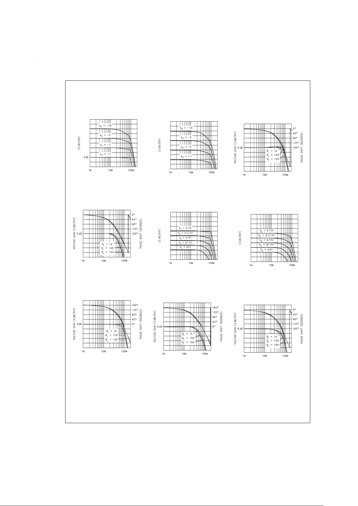
Typical Performance Characteristics T
A
=
25˚C unless otherwise noted
CLOSED-LOOP
FREQUENCY RESPONSE
V
S
=
±
15V; R
f
=
820Ω;
R
L
=
1kΩ
DS011328-34
CLOSED-LOOP
FREQUENCY RESPONSE
V
S
=
±
15V; R
f
=
820Ω;
R
L
=
150Ω
DS011328-35
UNITY GAIN
FREQUENCY RESPONSE
V
S
=
±
15V; A
V
=
+1;
R
f
=
820Ω
DS011328-36
UNIT GAIN
FREQUENCY RESPONSE
V
S
=
±
5V; A
V
=
+1;
R
f
=
820Ω
DS011328-37
FREQUENCY RESPONSE
vs SUPPLY VOLTAGE
A
V
=
−1; R
f
=
820Ω;
R
L
=
1kΩ
DS011328-38
FREQUENCY RESPONSE
vs SUPPLY VOLTAGE
A
V
=
−1; R
f
=
820Ω;
R
L
=
150Ω
DS011328-39
INVERTING GAIN
FREQUENCY RESPONSE
V
S
=
±
15V; A
V
=
−1;
R
f
=
820Ω
DS011328-40
INVERTING GAIN
FREQUENCY RESPONSE
V
S
=
±
5V; A
V
=
−1;
R
f
=
820Ω
DS011328-41
NON-INVERTING GAIN
FREQUENCY RESPONSE
V
S
=
±
15V; A
V
=
+2;
R
f
=
820Ω
DS011328-42
www.national.com 6
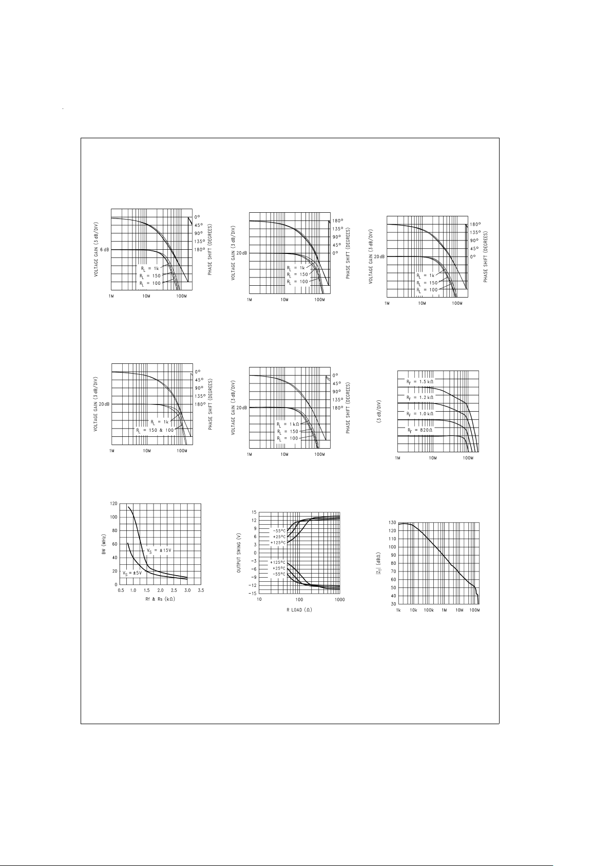
Typical Performance Characteristics T
A
=
25˚C unless otherwise noted (Continued)
NON-INVERTING GAIN
FREQUENCY RESPONSE
V
S
=
±
5V; A
V
=
+2;
R
f
=
820Ω
DS011328-43
INVERTING GAIN
FREQUENCY RESPONSE
V
S
=
±
15V; A
V
=
−10;
R
f
=
820Ω
DS011328-44
INVERTING GAIN
FREQUENCY RESPONSE
V
S
=
±
5V; A
V
=
−10;
R
f
=
820Ω
DS011328-45
NON-INVERTING GAIN
FREQUENCY RESPONSE
V
S
=
±
15V; A
V
=
+10;
R
f
=
820Ω
DS011328-46
NON-INVERTING GAIN
FREQUENCY RESPONSE
V
S
=
±
5V; A
V
=
+10;
R
f
=
820Ω
DS011328-47
NON-INVERTING GAIN
FREQUENCY COMPENSATION
V
S
=
±
15V; A
V
=
+2;
R
L
=
150Ω
DS011328-48
BANDWIDTH vs Rf&R
S
A
V
=
−1, R
L
=
1kΩ
DS011328-49
OUTPUT SWING vs
R
LOAD
PULSED, V
S
=
±
15V,
I
IN
=
±
200 µA, V
IN+
=
0V
DS011328-50
TRANSIMPEDANCE
vs FREQUENCY
V
S
=
±
15V
R
L
=
1kΩ
DS011328-51
www.national.com7
 Loading...