

LM6171
High Speed Low Power Low Distortion Voltage Feedback
Amplifier
General Description
The LM6171 is a high speed unity-gain stable voltage feedback amplifier. It offers a high slew rate of 3600V/µs and a
unity-gain bandwidth of 100 MHz while consuming only 2.5
mA of supply current. The LM6171 has very impressive AC
and DC performance which is a great benefit for high speed
signal processing and video applications.
The
±
15V power supplies allow for large signal swings and
give greater dynamic range and signal-to-noise ratio. The
LM6171 has high output current drive, low SFDR and THD,
ideal for ADC/DAC systems. The LM6171 is specified for
±
5V operation for portable applications.
The LM6171 is built on National’s advanced VIP
™
III (Verti-
cally Integrated PNP) complementary bipolar process.
Features
(Typical Unless Otherwise Noted)
n Easy-To-Use Voltage Feedback Topology
n Very High Slew Rate: 3600V/µs
n Wide Unity-Gain-Bandwidth Product: 100 MHz
n −3 dB Frequency
@
A
V
=
+2: 62 MHz
n Low Supply Current: 2.5 mA
n High CMRR: 110 dB
n High Open Loop Gain: 90 dB
n Specified for
±
15V and±5V Operation
Applications
n Multimedia Broadcast Systems
n Line Drivers, Switchers
n Video Amplifiers
n NTSC, PAL
®
and SECAM Systems
n ADC/DAC Buffers
n HDTV Amplifiers
n Pulse Amplifiers and Peak Detectors
n Instrumentation Amplifier
n Active Filters
Typical Performance Characteristics
VIP™is a trademark of National Semiconductor Corporation.
PAL
®
is a registered trademark of and used under licence from Advanced Micro Devices, Inc.
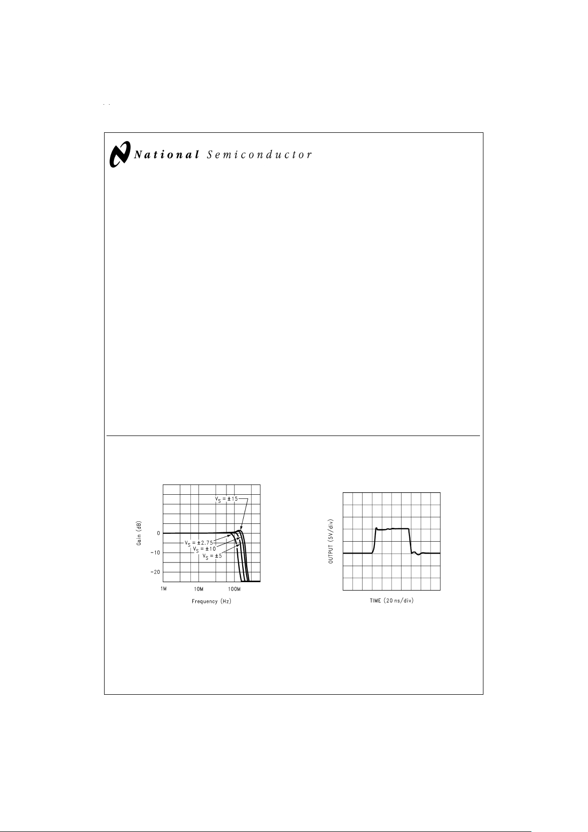
Closed Loop Frequency Response
vs Supply Voltage (A
V
=
+1)
DS012336-5
Large Signal
Pulse Response
A
V
=
+1, V
S
=
±
15
DS012336-9
May 1998
LM6171 High Speed Low Power Low Distortion Voltage Feedback Amplifier
© 1999 National Semiconductor Corporation DS012336 www.national.com
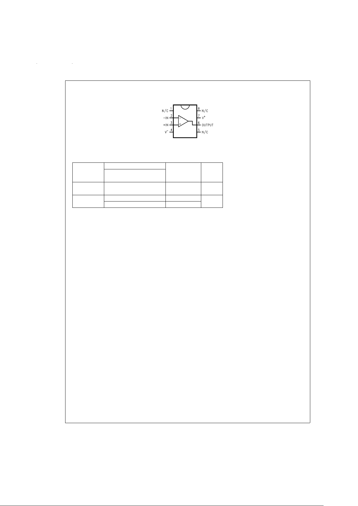
Connection Diagram
Ordering Information
Package Temperature Range Transport
Media
NSC
Drawing
Industrial
−40˚C to +85˚C
8-Pin LM6171AIN Rails N08E
Molded DIP LM6171BIN
8-Pin LM6171AIM, LM6171BIM Rails M08A
Small Outline LM6171AIMX, LM6171BIMX Tape and Reel
8-Pin DIP/SO
DS012336-1
Top View
www.national.com 2
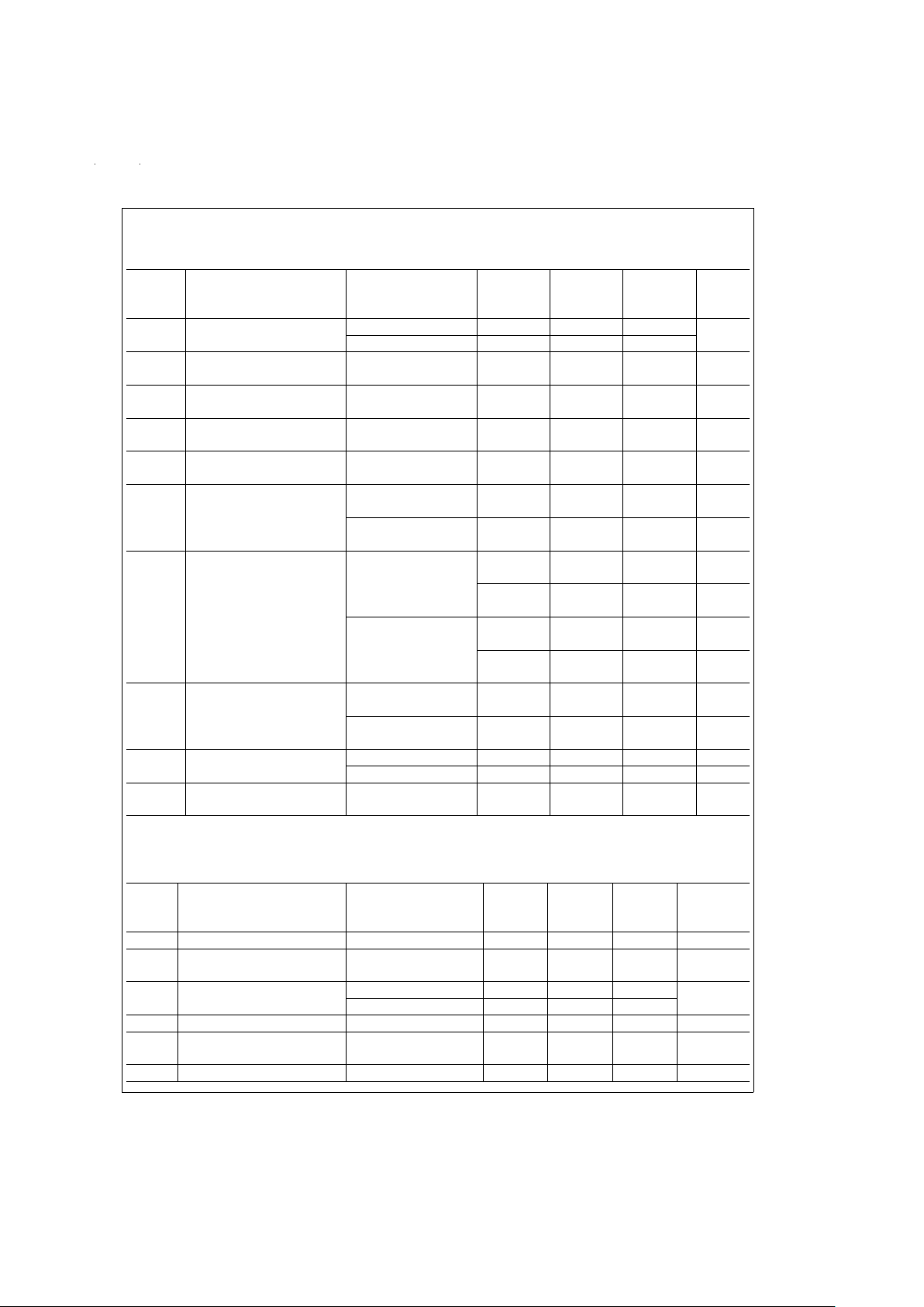
Absolute Maximum Ratings (Note 1)
If Military/Aerospace specified devices are required,
please contact the National Semiconductor Sales Office/
Distributors for availability and specifications.
ESD Tolerance (Note 2) 2.5 kV
Supply Voltage (V
+–V−
) 36V
Differential Input Voltage
(Note 11)
±
10V
Common-Mode
Voltage Range V
+
−1.4V to V−+ 1.4V
Output Short Circuit to Ground
(Note 3) Continuous
Storage Temperature Range −65˚C to +150˚C
Maximum Junction Temperature
(Note 4) 150˚C
Operating Ratings (Note 1)
Supply Voltage 2.75V ≤ V
+
≤ 18V
Junction Temperature Range
LM6171AI, LM6171BI −40˚C ≤ T
J
≤ +85˚C
Thermal Resistance (θ
JA
)
N Package, 8-Pin Molded DIP 108˚C/W
M Package, 8-Pin Surface Mount 172˚C/W
±
15V DC Electrical Characteristics
Unless otherwise specified, all limits guaranteed for T
J
=
25˚C, V
+
=
+15V, V
−
=
−15V, V
CM
=
0V, and R
L
=
1kΩ.Boldface
limits apply at the temperature extremes
Typ LM6171AI LM6171BI
Symbol Parameter Conditions (Note 5) Limit Limit Units
(Note 6) (Note 6)
V
OS
Input Offset Voltage 1.5 3 6 mV
58max
TC V
OS
Input Offset Voltage Average Drift 6 µV/˚C
I
B
Input Bias Current 1 3 3 µA
44max
I
OS
Input Offset Current 0.03 2 2 µA
33max
R
IN
Input Resistance Common Mode 40 MΩ
Differential Mode 4.9
R
O
Open Loop 14 Ω
Output Resistance
CMRR Common Mode V
CM
=
±
10V 110 80 75 dB
Rejection Ratio 75 70 min
PSRR Power Supply V
S
=
±
15V to±5V 95 85 80 dB
Rejection Ratio 80 75 min
V
CM
Input Common-Mode CMRR ≥ 60 dB
±
13.5 V
Voltage Range
A
V
Large Signal Voltage R
L
=
1kΩ 90 80 80 dB
Gain (Note 7) 70 70 min
R
L
=
100Ω 83 70 70 dB
60 60 min
V
O
Output Swing R
L
=
1kΩ 13.3 12.5 12.5 V
12 12 min
−13.3 −12.5 −12.5 V
−12 −12 max
R
L
=
100Ω 11.6 9 9 V
8.5 8.5 min
−10.5 −9 −9 V
−8.5 −8.5 max
Continuous Output Current Sourcing, R
L
=
100Ω 116 90 90 mA
(Open Loop) (Note 8) 85 85 min
Sinking, R
L
=
100Ω 105 90 90 mA
85 85 max
www.national.com3
±
15V DC Electrical Characteristics (Continued)
Unless otherwise specified, all limits guaranteed for T
J
=
25˚C, V
+
=
+15V, V
−
=
−15V, V
CM
=
0V, and R
L
=
1kΩ.Boldface
limits apply at the temperature extremes
Typ LM6171AI LM6171BI
Symbol Parameter Conditions (Note 5) Limit Limit Units
(Note 6) (Note 6)
Continuous Output Current Sourcing, R
L
=
10Ω 100 mA
(in Linear Region) Sinking, R
L
=
10Ω 80 mA
I
SC
Output Short Sourcing 135 mA
Circuit Current Sinking 135 mA
I
S
Supply Current 2.5 4 4 mA
4.5 4.5 max
±
15V AC Electrical Characteristics
Unless otherwise specified, all limits guaranteed for T
J
=
25˚C, V
+
=
+15V, V
−
=
−15V, V
CM
=
0V, and R
L
=
1kΩ.Boldface
limits apply at the temperature extremes
Typ LM6171AI LM6171BI
Symbol Parameter Conditions (Note 5) Limit Limit Units
(Note 6) (Note 6)
SR Slew Rate (Note 9) A
V
=
+2, V
IN
=
13 V
PP
3600 V/µs
A
V
=
+2, V
IN
=
10 V
PP
3000
GBW Unity Gain-Bandwidth Product 100 MHz
−3 dB Frequency A
V
=
+1 160 MHz
A
V
=
+2 62 MHz
φm Phase Margin 40 deg
t
s
Settling Time (0.1%)A
V
=
−1, V
OUT
=
±
5V 48 ns
R
L
=
500Ω
Propagation Delay V
IN
=
±
5V, R
L
=
500Ω,6 ns
A
V
=
−2
A
D
Differential Gain (Note 10) 0.03
%
φ
D
Differential Phase (Note 10) 0.5 deg
e
n
Input-Referred f=1 kHz
12
Voltage Noise
i
n
Input-Referred f=1 kHz
1
Current Noise
±
5V DC Electrical Characteristics
Unless otherwise specified, all limits guaranteed for T
J
=
25˚C, V
+
=
+5V, V
−
=
−5V, V
CM
=
0V, and R
L
=
1kΩ.Boldface
limits apply at the temperature extremes
Typ LM6171AI LM6171BI
Symbol Parameter Conditions (Note 5) Limit Limit Units
(Note 6) (Note 6)
V
OS
Input Offset Voltage 1.2 3 6 mV
58max
TC V
OS
Input Offset Voltage 4 µV/˚C
Average Drift
I
B
Input Bias Current 1 2.5 2.5 µA
3.5 3.5 max
I
OS
Input Offset Current 0.03 1.5 1.5 µA
2.2 2.2 max
www.national.com 4
±
5V DC Electrical Characteristics (Continued)
Unless otherwise specified, all limits guaranteed for T
J
=
25˚C, V
+
=
+5V, V
−
=
−5V, V
CM
=
0V, and R
L
=
1kΩ.Boldface
limits apply at the temperature extremes
Typ LM6171AI LM6171BI
Symbol Parameter Conditions (Note 5) Limit Limit Units
(Note 6) (Note 6)
R
IN
Input Resistance Common Mode 40 MΩ
Differential Mode 4.9
R
O
Open Loop 14 Ω
Output Resistance
CMRR Common Mode V
CM
=
±
2.5V 105 80 75 dB
Rejection Ratio 75 70 min
PSRR Power Supply V
S
=
±
15V to±5V 95 85 80 dB
Rejection Ratio 80 75 min
V
CM
Input Common-Mode CMRR ≥ 60 dB
±
3.7 V
Voltage Range
A
V
Large Signal Voltage R
L
=
1kΩ 84 75 75 dB
Gain (Note 7) 65 65 min
R
L
=
100Ω 80 70 70 dB
60 60 min
V
O
Output Swing R
L
=
1kΩ 3.5 3.2 3.2 V
33min
−3.4 −3.2 −3.2 V
−3 −3 max
R
L
=
100Ω 3.2 2.8 2.8 V
2.5 2.5 min
−3.0 −2.8 −2.8 V
−2.5 −2.5 max
Continuous Output Current Sourcing, R
L
=
100Ω 32 28 28 mA
(Open Loop) (Note 8) 25 25 min
Sinking, R
L
=
100Ω 30 28 28 mA
25 25 max
I
SC
Output Short Sourcing 130 mA
Circuit Current Sinking 100 mA
I
S
Supply Current 2.3 3 3 mA
3.5 3.5 max
±
5V AC Electrical Characteristics
Unless otherwise specified, all limits guaranteed for T
J
=
25˚C, V
+
=
+5V, V
−
=
−5V, V
CM
=
0V, and R
L
=
1kΩ.Boldface
limits apply at the temperature extremes
Typ LM6171AI LM6171BI
Symbol Parameter Conditions (Note 5) Limit Limit Units
(Note 6) (Note 6)
SR Slew Rate (Note 9) A
V
=
+2, V
IN
=
3.5 V
PP
750 V/µs
GBW Unity Gain-Bandwidth 70 MHz
Product
−3 dB Frequency A
V
=
+1 130 MHz
A
V
=
+2 45
φm Phase Margin 57 deg
t
s
Settling Time (0.1%)A
V
=
−1, V
OUT
=
+1V, 60 ns
R
L
=
500Ω
Propagation Delay V
IN
=
±
1V, R
L
=
500Ω,8 ns
www.national.com5
±
5V AC Electrical Characteristics (Continued)
Unless otherwise specified, all limits guaranteed for T
J
=
25˚C, V
+
=
+5V, V
−
=
−5V, V
CM
=
0V, and R
L
=
1kΩ.Boldface
limits apply at the temperature extremes
Typ LM6171AI LM6171BI
Symbol Parameter Conditions (Note 5) Limit Limit Units
(Note 6) (Note 6)
A
V
=
−2
A
D
Differential Gain (Note 10) 0.04
%
φ
D
Differential Phase (Note 10) 0.7 deg
e
n
Input-Referred f=1 kHz
11
Voltage Noise
i
n
Input-Referred f=1 kHz
1
Current Noise
Note 1: Absolute Maximum Ratings indicate limits beyond which damage to the device may occur. Operating Ratings indicate conditions for which the device is intended to be functional, but specific performance is not guaranteed. For guaranteed specifications and the test conditions, see the Electrical Characteristics.
Note 2: Human body model, 1.5 kΩ in series with 100 pF.
Note 3: Continuous short circuit operation at elevated ambient temperature can result in exceeding the maximum allowed junction temperature of 150˚C.
Note 4: The maximum power dissipation is a function of T
J(max)
, θJA, and TA. The maximum allowable power dissipation at any ambient temperature is P
D
=
(T
J(max)−TA
)/θJA. All numbers apply for packages soldered directly into a PC board.
Note 5: Typical Values represent the most likely parametric norm.
Note 6: All limits are guaranteed by testing or statistical analysis.
Note 7: Large signal voltage gain is the total output swing divided by the input signal required to produce that swing. For V
S
=
±
15V, V
OUT
=
±
5V. For V
S
=
+5V,
V
OUT
=
±
1V.
Note 8: The open loop output current is the output swing with the 100Ω load resistor divided by that resistor.
Note 9: Slew rate is the average of the rising and falling slew rates.
Note 10: Differential gain and phase are measured with A
V
=
+2, V
IN
=
1V
PP
at 3.58 MHz and both input and output 75Ω terminated.
Note 11: Differential input voltage is measured at V
S
=
±
15V.
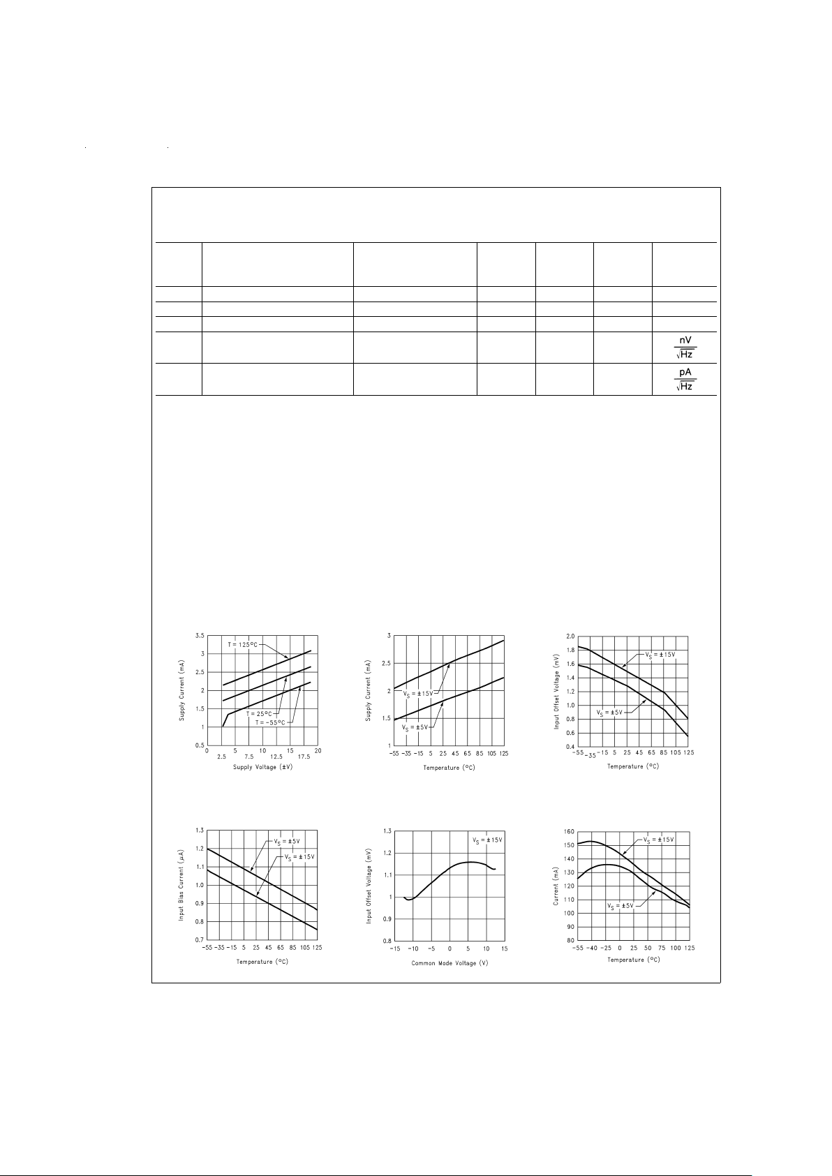
Typical Performance Characteristics Unless otherwise noted, T
A
=
25˚C
Supply Current vs
Supply Voltage
DS012336-20
Supply Current vs
Temperature
DS012336-21
Input Offset Voltage vs
Temperature
DS012336-22
Input Bias Current
vs Temperature
DS012336-23
Input Offset Voltage vs
Common Mode Voltage
DS012336-24
Short Circuit Current
vs Temperature (Sourcing)
DS012336-25
www.national.com 6
 Loading...