


LM6152/LM6154
Dual and Quad High Speed/Low Power 75 MHz GBW
Rail-to-Rail I/O Operational Amplifiers
General Description
Using patented circuit topologies, the LM6152/54 provides
new levels of speed vs. power performance in applications
where low voltage supplies or power limitations previously
made compromise necessary. With only 1.4 mA/amplifier
supply current, the 75 MHz gain bandwidth of this device
supports new portable applications where higher power devices unacceptably drainbatterylife. The slew rate of the devices increases with increasing input differential voltage,
thus allowing the device to handle capacitive loads while
maintaining large signal amplitude.
The LM6152/54 can be driven by voltages that exceed both
power supply rails, thus eliminating concerns about exceeding the common-mode voltage range. The rail-to-rail output
swing capability provides the maximum possible dynamic
range at the output. This is particularly important when operating on low supply voltages.
Operating on supplies from 2.7V to over 24V,the LM6152/54
is excellent for a very wide range of applications, from battery operated systems with large bandwidth requirements to
high speed instrumentation.
Features
At V
S
=
5V, Typ unless noted
n Greater than Rail-to-Rail Input CMVR −0.25V to 5.25V
n Rail-to-Rail Output Swing 0.01V to 4.99V
n Wide Gain-Bandwidth: 75 MHz
@
100 kHz
n Slew Rate:
Small signal 5V/µs
Large signal 45V/µs
n Low supply current 1.4mA/amplifier
n Wide supply range 2.7V to 24V
n Fast settling time of 1.1µs for 2V step (to 0.01%)
n PSRR 91 dB
n CMRR 84 dB
Applications
n Portable high speed instrumentation
n Signal conditioning amplifier/ADC buffers
n Barcode scanners
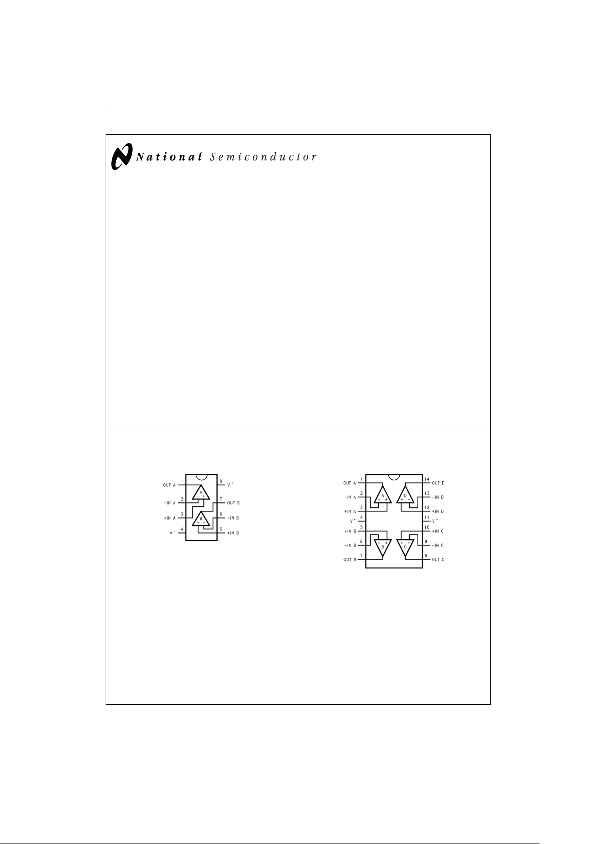
Connection Diagrams
8-Pin DIP/SO
DS012350-3
Top View
14-Pin DIP/SO
DS012350-4
Top View
May 1999
LM6152/LM6154Dual and Quad High Speed/Low Power 75 MHz GBW Rail-to-Rail I/O Operational
Amplifiers
© 1999 National Semiconductor Corporation DS012350 www.national.com
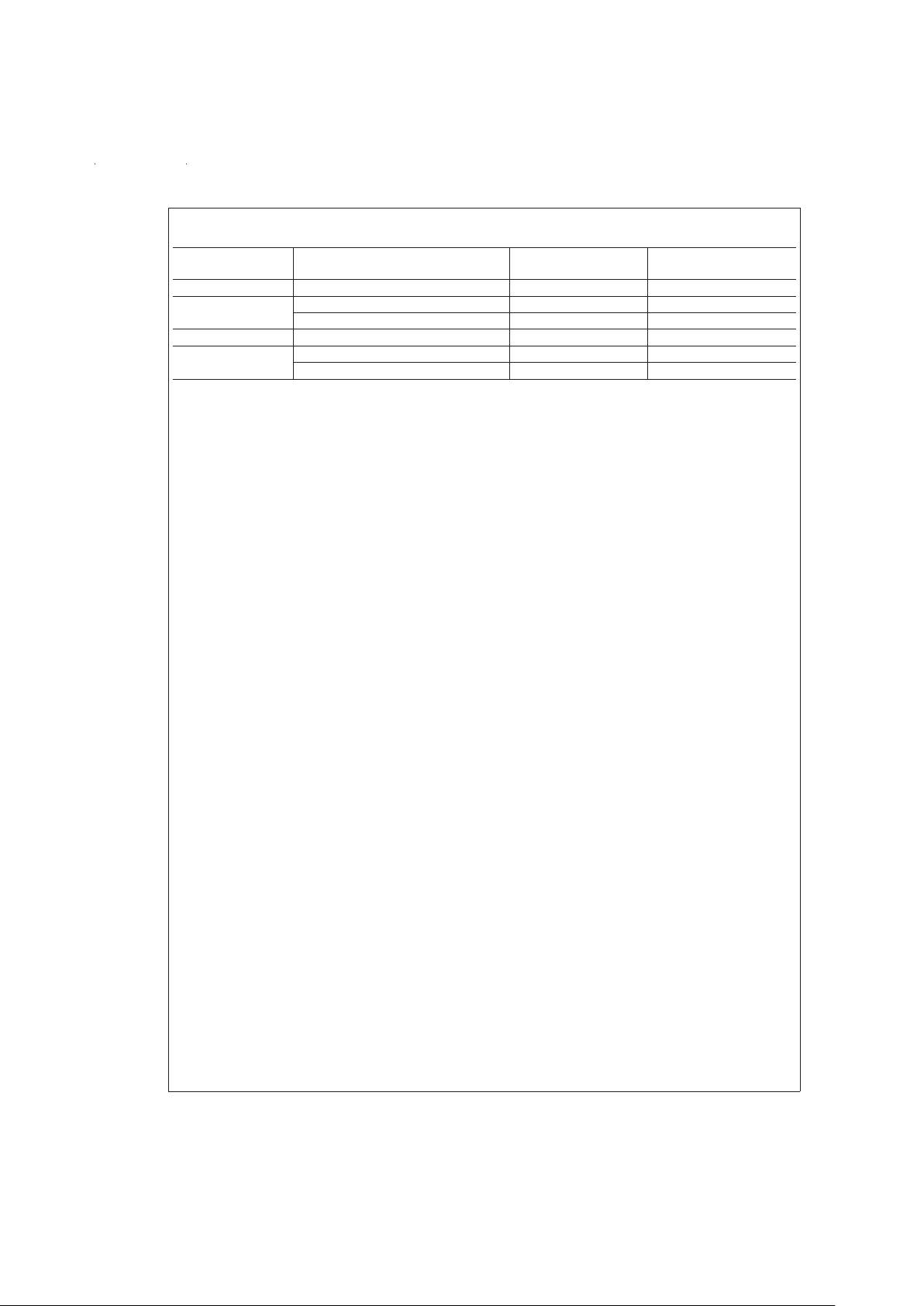
Ordering Information
Packaged Ordering Infomation
NSC Drawing
Number
Supplied As
8-Pin Dip LM6152ACN, LM5152BCN N08E Rails
8-Pin SOIC
LM6152ACM, LM6152BCM M08A Rails
LM6152ACMX, LM6152BCMX M08A 2.5k Tape and Reel
14-Pin DIP LM6154ACN, LM6154BCN N14A Rails
14-Pin SOIC
LM6154ACM, LM6154BCM M14A Rails
LM6154ACMX, LM6154BCMX M14A 2.5k Tape and Reel
www.national.com 2
Absolute Maximum Ratings (Note 1)
If Military/Aerospace specified devices are required,
please contact the National Semiconductor Sales Office/
Distributors for availability and specifications.
ESD Tolerance (Note 2) 2500V
Differential Input Voltage 15V
Voltage at Input/Output
Pin (V
+
) + 0.3V, (V−) −0.3V
Supply Voltage (V
+−V−
) 35V
Current at Input Pin
±
10mA
Current at Output Pin
(Note 3)
±
25mA
Current at Power Supply
Pin 50mA
Lead Temperature
(soldering, 10 sec) 260˚C
Storage Temperature
Range -65˚C to +150˚C
Junction Temperature
(Note 4) 150˚C
Operating Ratings (Note 1)
Supply Voltage 2.7V ≤ V
S
≤ 24V
Junction Temperature Range
LM6152,LM6154 0˚C ≤ T
J
≤ + 70˚C
Thermal Resistance (θ
JA
)
N Pkg, 8-pin Molded Dip 115˚C/W
M Pkg, 8-pin Surface Mount 193˚C/W
N Pkg, 14-pin Molded Dip 81˚C/W
M Pkg, 14-pin Surface Mount 126˚C/W
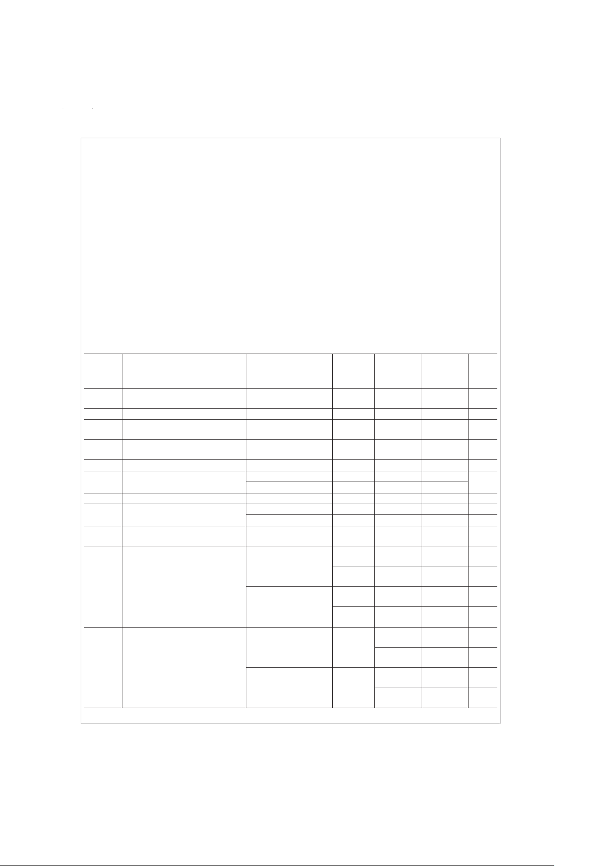
5.0V DC Electrical Characteristics
Unless otherwise specified, all limits guaranteed for TJ= 25˚C, V
+
=
5.0V, V
−
= 0V, V
CM
=
V
O
=
V
+
/2 and R
L
>
1MΩto V+/2.
Boldface limits apply at the temperature extremes.
Symbol Parameter Conditions
Typ
(Note 5)
LM6154AC
LM6152AC
Limit
(Note 6)
LM6154BC
LM6152BC
Limt
(Note 6)
Units
V
OS
Input Offset Voltage
0.54
2
4
5
7
mV
max
TCV
OS
Input Offset Voltage Average Drift 10 µV/˚C
I
B
Input Bias Current 0V ≤ VCM≤ 5V 500
750
980
1500
980
1500
nA
max
I
OS
Input Offset Current 32
40
100
160
100
160
nA
max
R
IN
Input Resistance, CM 0V ≤ VCM≤ 4V 30 MΩ
CMRR Common Mode Rejection Ratio 0V ≤ V
CM
≤ 4V 94 70 70
dB min
0V ≤ V
CM
≤ 5V 84 60 60
PSRR Power Supply Rejection Ratio 5V ≤ V
+
≤ 24V 91 80 80 dB min
V
CM
Input Common-Mode Voltage Range Low −0.25 0 0 V
High 5.25 5.0 5.0 V
A
V
Large Signal Voltage Gain R
L
=
10kΩ 214 50 50 V/mV
min
V
O
Output Swing
R
L
=
100kΩ
0.006
0.02
0.03
0.02
0.03
V
max
4.992
4.97
4.96
4.97
4.96
V
min
R
L
=
2kΩ
0.04
0.10
0.12
0.10
0.12
V
max
4.89
4.80
4.70
4.80
4.70
V
min
I
SC
Output Short Circuit Current Sourcing
6.2
3
2.5
3
2.5
mA
min
27
17
27
17
mA
max
Sinking
16.9
7
5
7
5
mA
min
40 40
mA
max
www.national.com3
5.0V DC Electrical Characteristics (Continued)
Unless otherwise specified, all limits guaranteed for TJ= 25˚C, V
+
=
5.0V, V
−
= 0V, V
CM
=
V
O
=
V
+
/2 and R
L
>
1MΩto V+/2.
Boldface limits apply at the temperature extremes.
Symbol Parameter Conditions
Typ
(Note 5)
LM6154AC
LM6152AC
Limit
(Note 6)
LM6154BC
LM6152BC
Limt
(Note 6)
Units
I
S
Supply Current Per Amplifier
1.4
2
2.25
2
2.25
mA
max
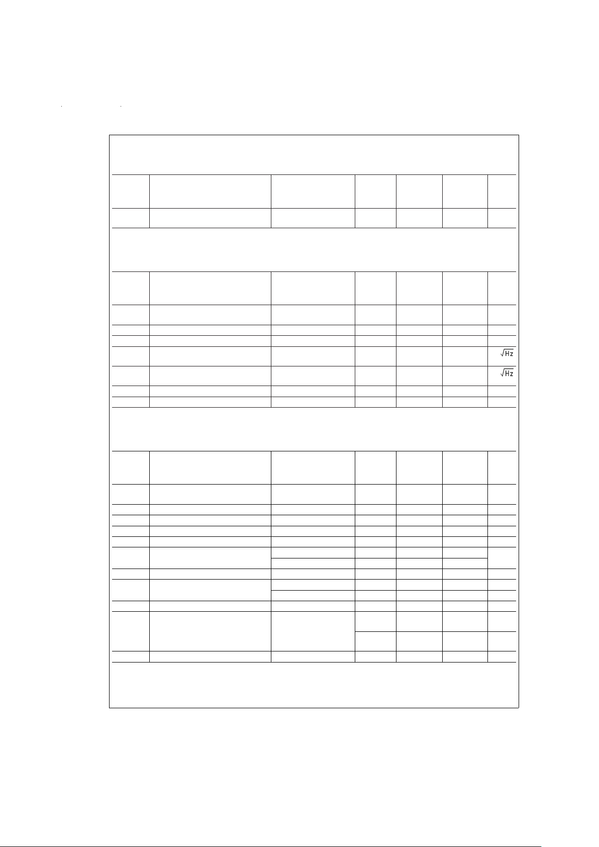
5.0V AC Electrical Characteristics
Unless otherwise specified, all limits guaranteed for TJ= 25˚C, V
+
=
5.0V, V
−
= 0V, V
CM
=
V
O
=
V
+
/2 and R
L
>
1MΩto V+/2.
Boldface limits apply at the temperature extremes.
Symbol Parameter Conditions
Typ
(Note 5)
LM6154AC
LM6152AC
Limit
(Note 6)
LM6154BC
LM6152BC
Limt
(Note 6)
Units
SR Slew Rate
±
4V Step@V
S
=
±
6V,
R
S
<
1kΩ
30
24
15
24
15
V/µs
min
GBW Gain-Bandwidth Product f=100 kHz 75 MHz
Amp-to-Amp Isolation R
L
=
10kΩ 125 dB
e
n
Input-Referred Voltage Noise f=1 kHz 9 nV
i
n
Input-Referred Current Noise f=1 kHz 0.34 pA
T.H.D Total Harmonic Distortion f=10 kHz, R
L
=
10kΩ 0.002
%
ts Settling Time 2V Step to 0.01
%
1.1 µs
2.7V DC Electrical Characteristics
Unless otherwise specified, all limits guaranteed for TJ= 25˚C, V
+
=
2.7V, V
−
= 0V, V
CM
=
V
O
=V+/2 and R
L
>
1MΩto V+/2.
Boldface limits apply at the temperature extremes.
Symbol Parameter Conditions
Typ
(Note 5)
LM6154AC
LM6152AC
Limit
(Note 6)
LM6154BC
LM6152BC
Limt
(Note 6)
Units
V
OS
Input Offset Voltage
0.8
2
5
5
8
mV
max
TCV
OS
Input Offset Voltage Average Drift 10 µV/˚C
I
B
Input Bias Current 500 nA
I
OS
Input Offset Current 50 nA
R
IN
Input Resistance, CM 0V ≤ VCM≤ 1.8V 30 MΩ
CMRR Common Mode Rejection Ratio 0V ≤ V
CM
≤ 1.8V 88
dB
0V ≤ V
CM
≤ 2.7V 78
PSRR Power Supply Rejection Ratio 3V ≤ V
+
≤ 5V 69 dB
V
CM
Input Common-Mode Voltage Range Low −0.25 0 0 V
High 2.95 2.7 2.7 V
A
V
Large Signal Voltage Gain R
L
=
10kΩ 5.5 V/mV
V
O
Output Swing R
L
=
10kΩ
0.032
0.07
0.11
0.07
0.11
V
max
2.68
2.64
2.62
2.64
2.62
V
min
I
S
Supply Current Per Amplifier 1.35 mA
www.national.com 4