

NSC LM6144AIMX, LM6144AIM, LM6144BIN, LM6144BIM, LM6144AIN Datasheet
...
LM6142 Dual and LM6144 Quad
High Speed/Low Power 17 MHz Rail-to-Rail Input-Output
Operational Amplifiers
General Description
Using patent pending new circuit topologies, the LM6142/44
provides new levels of performance in applications where
low voltage supplies or power limitations previously made
compromise necessary. Operating on supplies of 1.8V to
over 24V, the LM6142/44 is an excellent choice for battery
operated systems, portable instrumentation and others.
The greater than rail-to-rail input voltage range eliminates
concern over exceeding the common-mode voltage range.
The rail-to-rail output swing provides the maximum possible
dynamic range at the output. This is particularly important
when operating on low supply voltages.
High gain-bandwidth with 650 µA/Amplifier supply current
opens new battery powered applications where previous
higher power consumption reduced battery life to unacceptable levels. Theabilityto drive large capacitive loads without
oscillating functionally removes this common problem.
Features
At V
S
=
5V. Typ unless noted.
n Rail-to-rail input CMVR −0.25V to 5.25V
n Rail-to-rail output swing 0.005V to 4.995V
n Wide gain-bandwidth: 17 MHz at 50 kHz (typ)
n Slew rate:
Small signal, 5V/µs
Large signal, 30V/µs
n Low supply current 650 µA/Amplifier
n Wide supply range 1.8V to 24V
n CMRR 107 dB
n Gain 108 dB with R
L
=
10k
n PSRR 87 dB
Applications
n Battery operated instrumentation
n Depth sounders/fish finders
n Barcode scanners
n Wireless communications
n Rail-to-rail in-out instrumentation amps
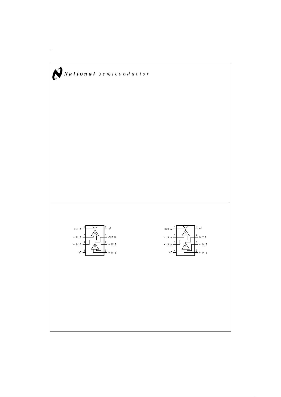
Connection Diagrams
8-Pin CDIP
DS012057-14
Top View
8-Pin DIP/SO
DS012057-1
Top View
May 1999
LM6142 Dual and LM6144 Quad High Speed/Low Power 17 MHz Rail-to-Rail Input-Output
Operational Amplifiers
© 1999 National Semiconductor Corporation DS012057 www.national.com
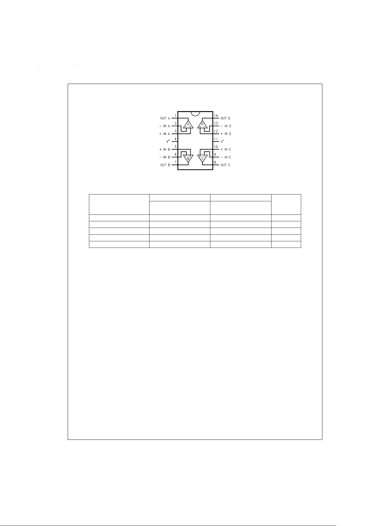
Connection Diagrams (Continued)
Ordering Information
Package Temperature Range Temperature Range NSC
Drawing
Industrial Military
−40˚C to +85˚C −55˚C to +125˚C
8-Pin Molded DIP LM6142AIN, LM6142BIN N08E
8-Pin Small Outline LM6142AIM, LM6142BIM M08A
14-Pin Molded DIP LM6144AIN, LM6144BIN N14A
14-Pin Small Outline LM6144AIM, LM6144BIM M14A
8-Pin CDIP LM6142AMJ-QML J08A
14-Pin DIP/SO
DS012057-2
Top View
www.national.com 2
Absolute Maximum Ratings (Note 1)
If Military/Aerospace specified devices are required,
please contact the National Semiconductor Sales Office/
Distributors for availability and specifications.
ESD Tolerance (Note 2) 2500V
Differential Input Voltage 15V
Voltage at Input/Output Pin (V+) + 0.3V, (V−) − 0.3V
Supply Voltage (V+ − V−) 35V
Current at Input Pin
±
10 mA
Current at Output Pin (Note 3)
±
25 mA
Current at Power Supply Pin 50 mA
Lead Temperature
(soldering, 10 sec) 260˚C
Storage Temp. Range −65˚C to +150˚C
Junction Temperature (Note 4) 150˚C
Operating Ratings (Note 1)
Supply Voltage 1.8V ≤ V+ ≤ 24V
Junction Temperature Range
LM6142, LM6144 −40˚C ≤ T
J
≤ +85˚C
Thermal Resistance (θ
JA
)
N Package, 8-Pin Molded DIP 115˚C/W
M Package, 8-Pin Surface Mount 193˚C/W
N Package, 14-Pin Molded DIP 81˚C/W
M Package, 14-Pin Surface Mount 126˚C/W
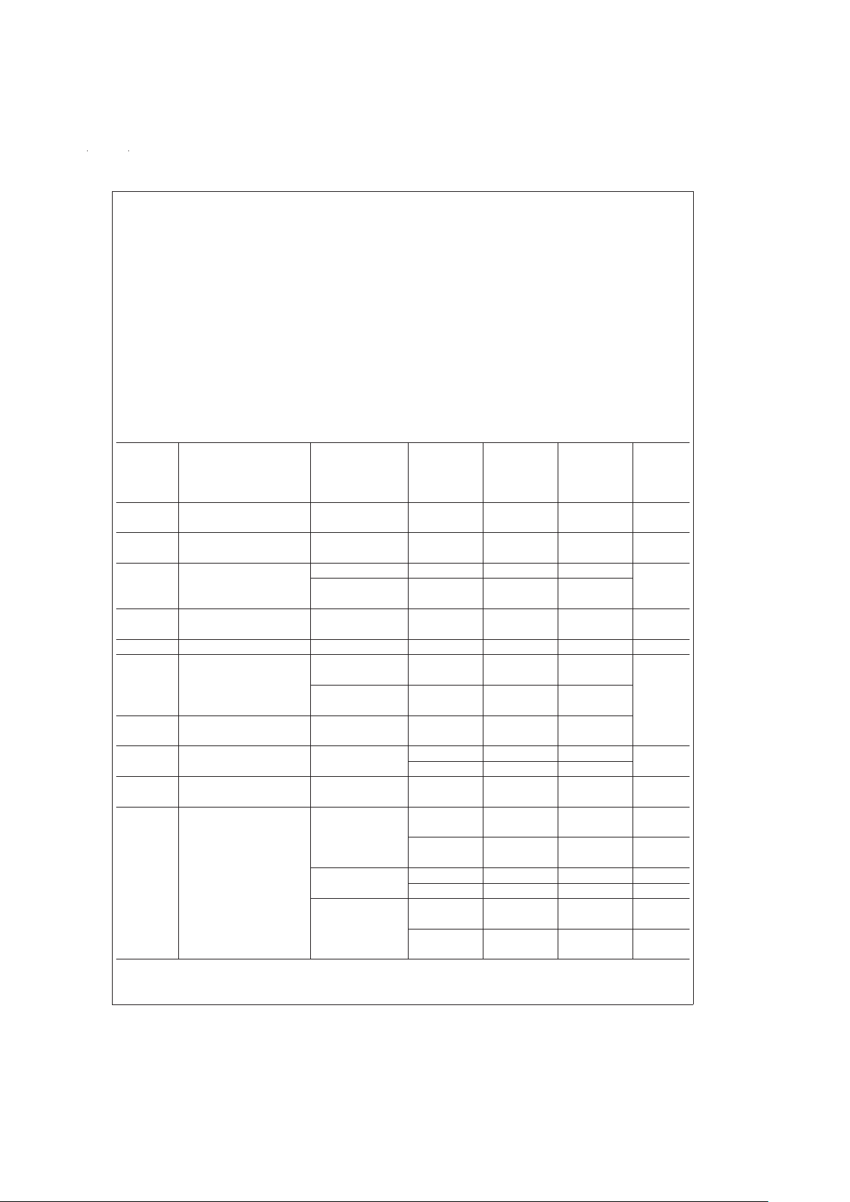
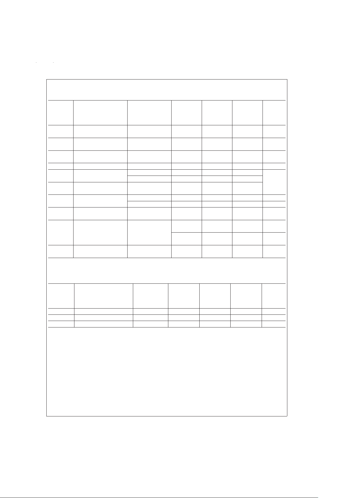
5.0V DC Electrical Characteristics
Unless otherwise specified, all limits guaranteed for T
J
=
25˚C, V+=5.0V, V−=0V, V
CM
=
V
O
=
V+/2 and R
L
>
1MΩto
V+/2. Boldface limits apply at the temperature extremes.
LM6144AI LM6144BI
Symbol Parameter Conditions Typ LM6142AI LM6142BI Units
(Note 5) Limit Limit
(Note 6) (Note 6)
V
OS
Input Offset Voltage 0.3 1.0 2.5 mV
2.2 3.3 max
TCV
OS
Input Offset Voltage 3 µV/˚C
Average Drift
I
B
Input Bias Current 170 250 300 nA
max
0V ≤ V
CM
≤ 5V 180 280
526 526
I
OS
Input Offset Current 3 30 30 nA
80 80 max
R
IN
Input Resistance, C
M
126 MΩ
CMRR Common Mode 0V ≤ V
CM
≤ 4V 107 84 84
dB
min
Rejection Ratio 78 78
0V ≤ V
CM
≤ 5V 82 66 66
79 64 64
PSRR Power Supply 5V ≤ V
+
≤ 24V 87 80 80
Rejection Ratio 78 78
V
CM
Input Common-Mode −0.25 00V
Voltage Range 5.25 5.0 5.0
A
V
Large Signal R
L
=
10k 270 100 80 V/mV
Voltage Gain 70 33 25 min
V
O
Output Swing R
L
=
100k 0.005 0.01 0.01 V
0.013 0.013 max
4.995 4.98 4.98 V
4.93 4.93 min
R
L
=
10k 0.02 V max
4.97 V min
R
L
=
2k 0.06 0.1 0.1 V
0.133 0.133 max
4.90 4.86 4.86 V
4.80 4.80 min
www.national.com3
5.0V DC Electrical Characteristics (Continued)
Unless otherwise specified, all limits guaranteed for T
J
=
25˚C, V+=5.0V, V−=0V, V
CM
=
V
O
=
V+/2 and R
L
>
1MΩto
V+/2. Boldface limits apply at the temperature extremes.
LM6144AI LM6144BI
Symbol Parameter Conditions Typ LM6142AI LM6142BI Units
(Note 5) Limit Limit
(Note 6) (Note 6)
I
SC
Output Short Sourcing 13 10 8 mA
Circuit Current 4.9 4 min
LM6142 35 35 mA
max
Sinking 24 10 10 mA
5.3 5.3 min
35 35 mA
max
I
SC
Output Short Sourcing 8 6 6 mA
Circuit Current 33min
LM6144 35 35 mA
max
Sinking 22 8 8 mA
44min
35 35 mA
max
I
S
Supply Current Per Amplifier 650 800 800 µA
880 880 max
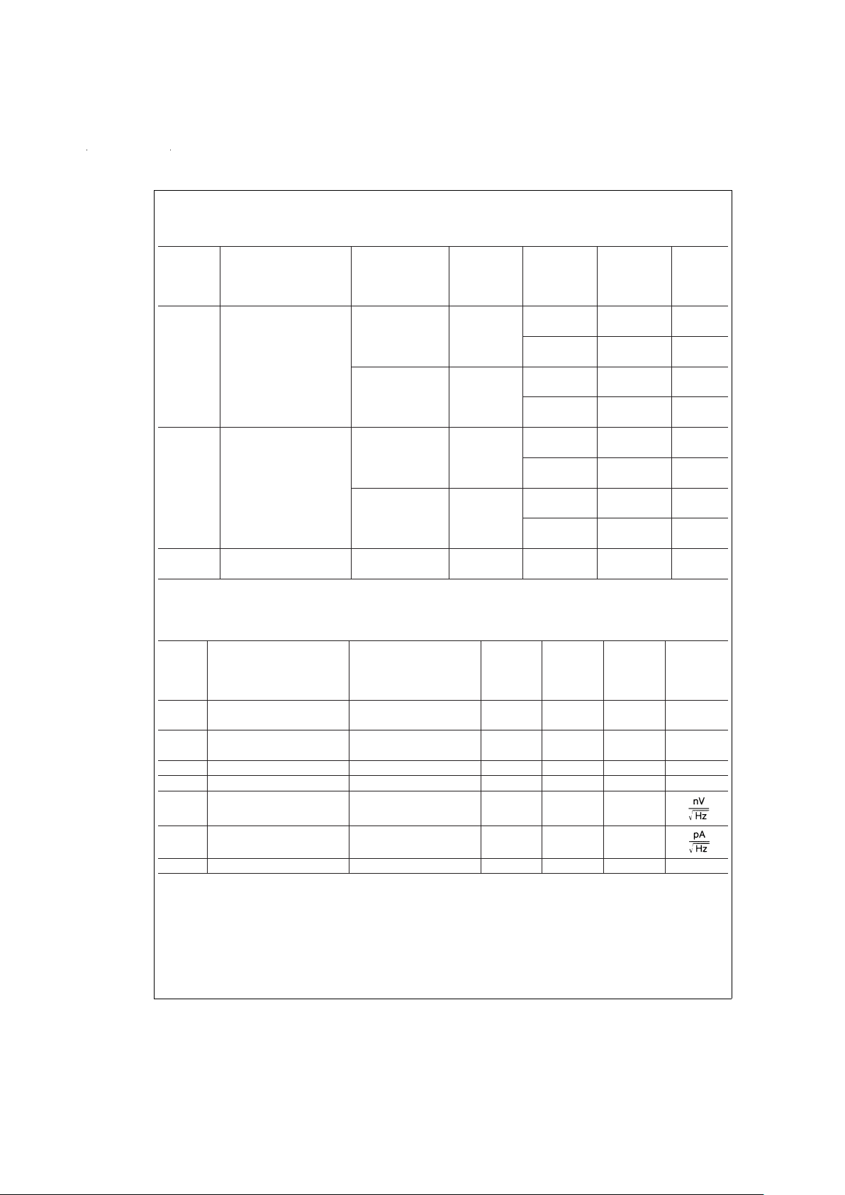
5.0V AC Electrical Characteristics
Unless Otherwise Specified, All Limits Guaranteed for T
J
=
25˚C, V+=5.0V, V−=0V, V
CM
=
V
O
=
V+/2 and R
L
>
1MΩto
V
S
/2. Boldface limits apply at the temperature extremes.
LM6144AI LM6144BI
Symbol Parameter Conditions Typ LM6142AI LM6142BI Units
(Note 5) Limit Limit
(Note 6) (Note 6)
SR Slew Rate 8 V
p-p
@
VCC12V 25 15 13 V/µs
R
S
>
1kΩ 13 11 min
GBW Gain-Bandwidth Product f=50 kHz 17 10 10 MHz
66min
φ
m
Phase Margin 38 Deg
Amp-to-Amp Isolation 130 dB
e
n
Input-Referred f=1 kHz
16
Voltage Noise
i
n
Input-Referred f=1 kHz
0.22
Current Noise
T.H.D. Total Harmonic Distortion f=10 kHz, R
L
=
10 kΩ, 0.003
%
www.national.com 4
2.7V DC Electrical Characteristics
Unless Otherwise Specified, All Limits Guaranteed for T
J
=
25˚C, V+=2.7V, V−=0V, V
CM
=
V
O
=
V+/2 and R
L
>
1MΩto
V+/2. Boldface limits apply at the temperature extreme
LM6144AI LM6144BI
Symbol Parameter Conditions Typ LM6142AI LM6142BI Units
(Note 5) Limit Limit
(Note 6) (Note 6)
V
OS
Input Offset Voltage 0.4 1.8 2.5 mV
4.3 4.3 max
I
B
Input Bias Current 150 250 300 nA
526 526 max
I
OS
Input Offset Current 4 30 30 nA
80 80 max
R
IN
Input Resistance 128 MΩ
CMRR Common Mode 0V ≤ V
CM
≤ 1.8V 90 dB
min
Rejection Ratio 0V ≤ V
CM
≤ 2.7V 76
PSRR Power Supply 3V ≤ V+ ≤ 5V 79
Rejection Ratio
V
CM
Input Common-Mode −0.25 0 0 V min
Voltage Range 2.95 2.7 2.7 V max
A
V
Large Signal R
L
=
10k 55 V/mV
Voltage Gain min
V
O
Output Swing R
L
=
10 kΩ 0.019 0.08 0.08 V
0.112 0.112 max
2.67 2.66 2.66 V
2.25 2.25 min
I
S
Supply Current Per Amplifier 510 800 800 µA
880 880 max
2.7V AC Electrical Characteristics
Unless Otherwise Specified, All Limits Guaranteed for T
J
=
25˚C, V+=2.7V, V−=0V, V
CM
=
V
O
=
V+/2 and R
L
>
1MΩto
V+/2. Boldface limits apply at the temperature extreme
LM6144AI LM6144BI
Symbol Parameter Conditions Typ LM6142AI LM6142BI Units
(Note 5) Limit Limit
(Note 6) (Note 6)
GBW Gain-Bandwidth Product f=50 kHz 9 MHz
φ
m
Phase Margin 36 Deg
G
m
Gain Margin 6 dB
www.national.com5
 Loading...