

NSC LM613IWMX, LM613AMJ-883, LM613IWM Datasheet
LM613
Dual Operational Amplifiers, Dual Comparators, and
Adjustable Reference
General Description
The LM613 consists of dual op-amps, dual comparators, and
a programmable voltage reference in a 16-pin package. The
op-amps out-performs most single-supply op-amps by providing higher speed and bandwidth along with low supply
current. This device was specifically designed to lower cost
and board space requirements in transducer, test, measurement, and data acquisition systems.
Combining a stable voltage reference with wide output swing
op-amps makes the LM613 ideal for single supply transducers, signal conditioning and bridge driving where large
common-mode-signals are common. The voltage reference
consists of a reliable band-gap design that maintains low dynamic output impedance (1Ω typical), excellent initial tolerance (0.6%), and the ability to be programmed from 1.2V to
6.3V via two external resistors. The voltage reference is very
stable even when driving large capacitive loads, as are commonly encountered in CMOS data acquisition systems.
As a member of National’s Super-Block
™
family, the LM613
is a space-saving monolithic alternative to a multi-chip solution, offering a high level of integration without sacrificing
performance.
Features
OP AMP
n Low operating current (Op Amp): 300 µA
n Wide supply voltage range: 4V to 36V
n Wide common-mode range: V
−
to (V+− 1.8V)
n Wide differential input voltage:
±
36V
n Available in plastic package rated for Military Temp.
Range Operation
REFERENCE
n Adjustable output voltage: 1.2V to 6.3V
n Tight initial tolerance available:
±
0.6
%
n Wide operating current range: 17 µA to 20 mA
n Tolerant of load capacitance
Applications
n Transducer bridge driver
n Process and mass flow control systems
n Power supply voltage monitor
n Buffered voltage references for A/D’s
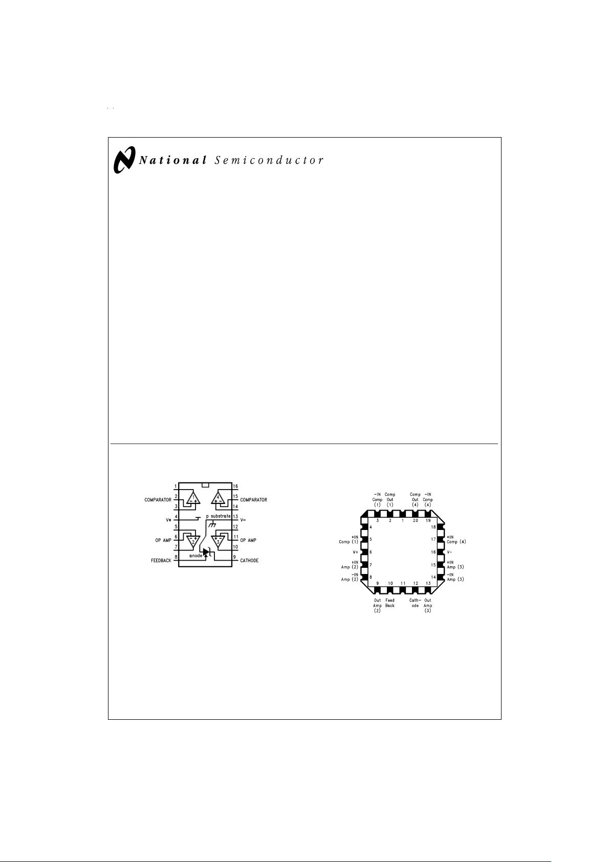
Connection Diagrams
Super-Block™is a trademark of NationalSemiconductor Corporation.
DS009226-1
Top View
E Package Pinout
DS009226-48
June 1998
LM613 Dual Operational Amplifiers, Dual Comparators, and Adjustable Reference
© 1999 National Semiconductor Corporation DS009226 www.national.com
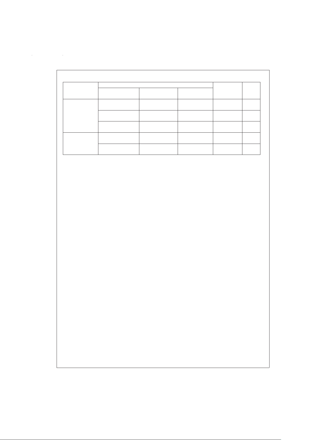
Ordering Information
Reference
Tolerance & V
OS
Temperature Range Package NSC
Drawing
Military Industrial Commercial
−55˚C ≤ T
A
≤ +125˚C −40˚C ≤ TA≤ +85˚C 0˚C ≤ TA≤ +70˚C
±
0.6
%
LM613AMN LM613AIN — 16-Pin N16E
80 ppm/˚C Max. Molded DIP
V
OS
≤ 3.5 mV LM613AMJ/883 — — 16-Pin J16A
(Note 14) Ceramic DIP
LM613AME/883 — — 20-Pin E20A
(Note 14) LCC
±
2.0
%
LM613MN LM613IN LM613CN 16-Pin N16E
150 ppm/˚C Max. Molded DIP
V
OS
≤ 5.0 mV Max. — LM613IWM 16-Pin Wide M16B
Surface Mount
www.national.com 2
Absolute Maximum Ratings (Note 1)
If Military/Aerospace specified devices are required,
please contact the National Semiconductor Sales Office/
Distributors for availability and specifications.
Voltage on Any Pin Except V
R
(referred to V−pin)
(Note 2)
(Note 3)
36V (Max)
−0.3V (Min)
Current through Any Input Pin
&V
R
Pin
±
20 mA
Differential Input Voltage
Military and Industrial
Commercial
±
36V
±
32V
Storage Temperature Range −65˚C ≤ T
J
≤ +150˚C
Maximum Junction Temp.(Note 4) 150˚C
Thermal Resistance,
Junction-to-Ambient (Note 5)
N Package
WM Package
100˚C/W
150˚C/W
Soldering Information (10 Sec.)
N Package
WM Package
260˚C
220˚C
ESD Tolerance (Note 6)
±
1kV
Operating Temperature Range
LM613AI, LM613BI: −40˚C to +85˚C
LM613AM, LM613M: −55˚C to +125˚C
LM613C: 0˚C ≤ T
J
≤ +70˚C
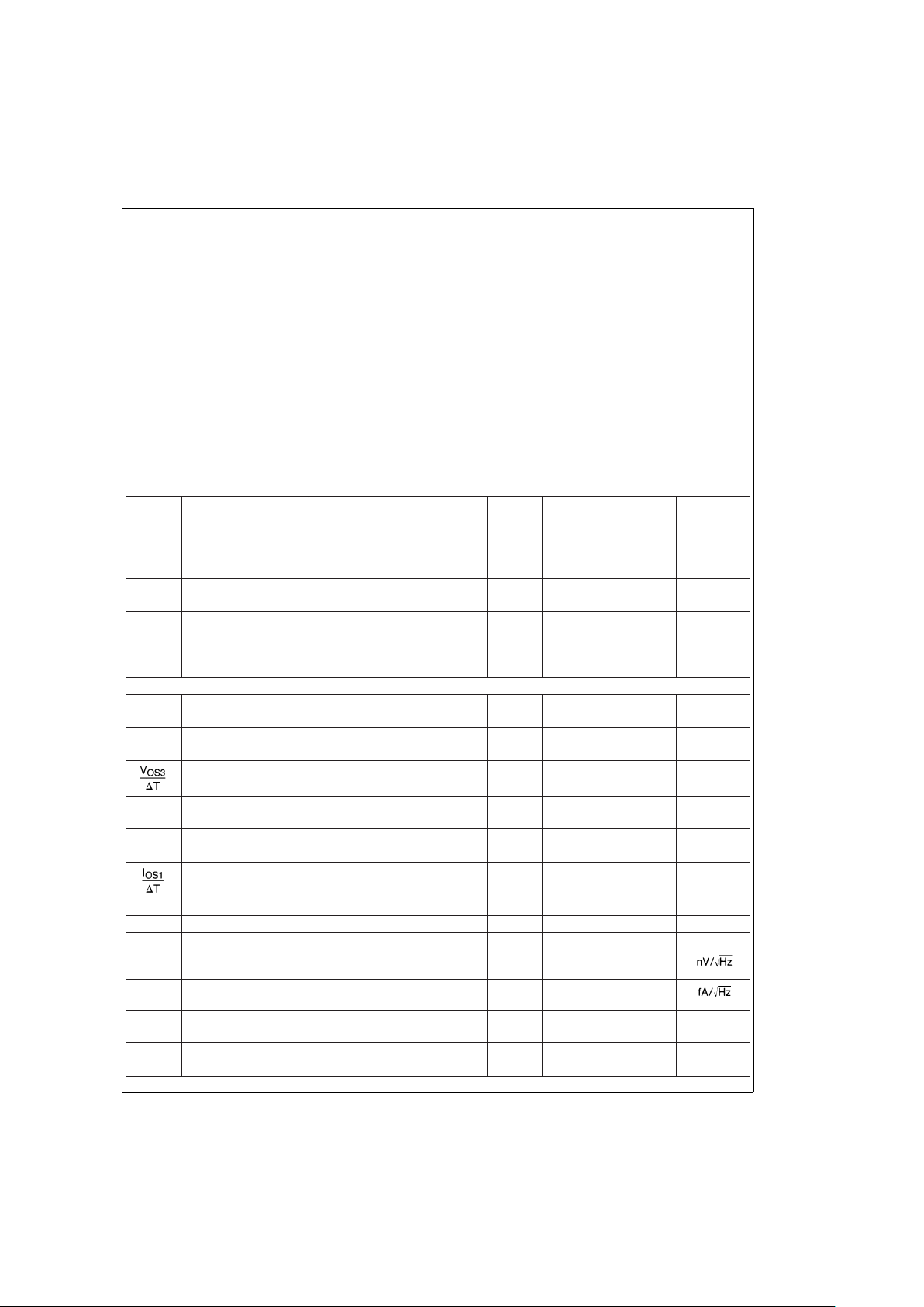
Electrical Characteristics
These specifications apply for V
−
=
GND=0V, V
+
=
5V, V
CM
=
V
OUT
=
2.5V, I
R
=
100 µA, FEEDBACK pin shorted to GND,
unless otherwise specified. Limits in standard typeface are for T
J
=
25˚C; limits in boldface type apply over the Operating
Temperature Range.
LM613AM LM613M
Typical LM613AI LM613I
Symbol Parameter Conditions (Note 7) Limits LM613C Units
(Note 8) Limits
(Note 8)
I
S
Total Supply Current R
LOAD
=
∞
, 450 940 1000 µA (Max)
4V ≤ V
+
≤ 36V (32V for LM613C) 550 1000 1070 µA (Max)
V
S
Supply Voltage Range 2.2 2.8 2.8 V (Min)
2.9 3 3 V (Min)
46 36 32 V (Max)
43 36 32 V (Max)
OPERATIONAL AMPLIFIERS
V
OS1
VOSOver Supply 4V ≤ V+≤ 36V 1.5 3.5 5.0 mV (Max)
(4V ≤ V
+
≤ 32V for LM613C) 2.0 6.0 7.0 mV (Max)
V
OS2
VOSOver V
CM
V
CM
=
0V through V
CM
=
1.0 3.5 5.0 mV (Max)
(V
+
− 1.8V), V
+
=
30V, V
−
=
0V 1.5 6.0 7.0 mV (Max)
Average VOSDrift (Note 8) 15 µV/˚C
(Max)
I
B
Input Bias Current 10 25 35 nA (Max)
11 30 40 nA (Max)
I
OS
Input Offset Current 0.2 4 4 nA (Max)
0.3 5 5 nA (Max)
Average Offset Current
4 pA/˚C
R
IN
Input Resistance Differential 1000 MΩ
C
IN
Input Capacitance Common-Mode 6 pF
e
n
Voltage Noise f=100 Hz, Input Referred 74
I
n
Current Noise f=100 Hz, Input Referred 58
CMRR Common-Mode V
+
=
30V, 0V ≤ V
CM
≤ (V+− 1.8V) 95 80 75 dB (Min)
Rejection Ratio CMRR=20 log (∆V
CM
/∆VOS) 90 75 70 dB (Min)
PSRR Power Supply 4V ≤ V
+
≤ 30V, V
CM
=
V
+
/2, 110 80 75 dB (Min)
Rejection Ratio PSRR=20 log (∆V
+
/VOS) 100 75 70 dB (Min)
www.national.com3
Electrical Characteristics (Continued)
These specifications apply for V
−
=
GND=0V, V
+
=
5V, V
CM
=
V
OUT
=
2.5V, I
R
=
100 µA, FEEDBACK pin shorted to GND,
unless otherwise specified. Limits in standard typeface are for T
J
=
25˚C; limits in boldface type apply over the Operating
Temperature Range.
LM613AM LM613M
Typical LM613AI LM613I
Symbol Parameter Conditions (Note 7) Limits LM613C Units
(Note 8) Limits
(Note 8)
OPERATIONAL AMPLIFIERS
A
V
Open Loop R
L
=
10 kΩ to GND, V
+
=
30V, 500 100 94 V/mV
Voltage Gain 5V ≤ V
OUT
≤ 25V 50 40 40 (Min)
SR Slew Rate V
+
=
30V (Note 9) 0.70 0.55 0.50 V/µs
0.65 0.45 0.45
GBW Gain Bandwidth C
L
=
50 pF 0.8 MHz
0.5 MHz
V
O1
Output Voltage R
L
=
10 kΩ to GND, V
+
− 1.4 V+− 1.7 V+− 1.8 V (Min)
Swing High V
+
=
36V (32V for LM613C) V
+
− 1.6 V+− 1.9 V+− 1.9 V (Min)
V
O2
Output Voltage R
L
=
10 kΩ to V
+
,V
−
+ 0.8 V−+ 0.9 V−+ 0.95 V (Max)
Swing Low V
+
=
36V (32V for LM613C) V
−
+ 0.9 V−+ 1.0 V−+ 1.0 V (Max)
I
OUT
Output Source Current V
OUT
=
2.5V, V
+
IN
=
0V, 25 20 16 mA (Min)
V
−
IN
=
−0.3V 15 13 13 mA (Min)
I
SINK
Output Sink Current V
OUT
=
1.6V, V
+
IN
=
0V, 17 14 13 mA (Min)
V
−
IN
=
0.3V 98 8mA (Min)
I
SHORT
Short Circuit Current V
OUT
=
0V,V
+
IN
=
3V, 30 50 50 mA (Max)
V
−
IN
=
2V 40 60 60 mA (Max)
V
OUT
=
5V, V
+
IN
=
2V, 30 60 70 mA (Max)
V
−
IN
=
3V 32 80 90 mA (Max)
COMPARATORS
V
OS
Offset Voltage 4V ≤ V+≤ 36V (32V for LM613C), 1.0 3.0 5.0 mV (Max)
R
L
=
15 kΩ 2.0 6.0 7.0 mV (Max)
Offset Voltage 0V ≤ VCM≤ 36V 1.0 3.0 5.0 mV (Max)
over V
CM
V
+
=
36V, (32V for LM613C) 1.5 6.0 7.0 mV (Max)
Average Offset 15 µV/˚C
Voltage Drift (Max)
I
B
Input Bias Current 5 25 35 nA (Max)
830 40nA (Max)
I
OS
Input Offset Current 0.2 4 4 nA (Max)
0.3 5 5 nA (Max)
A
V
Voltage Gain R
L
=
10 kΩ to 36V (32V for
LM613C)
500 V/mV
2V ≤ V
OUT
≤ 27V 100 V/mV
t
r
Large Signal V
+
IN
=
1.4V, V
−
IN
=
TTL Swing, 1.5 µs
Response Time R
L
=
5.1 kΩ 2.0 µs
I
SINK
Output Sink Current V
+
IN
=
0V, V
−
IN
=
1V, 20 10 10 mA (Min)
V
OUT
=
1.5V 13 8 8 mA (Min)
V
OUT
=
0.4V 2.8 1.0 0.8 mA (Min)
2.4 0.5 0.5 mA (Min)
I
LEAK
Output Leakage V
+
IN
=
1V, V
−
IN
=
0V, 0.1 10 10 µA (Max)
Current V
OUT
=
36V (32V for LM613C) 0.2 µA (Max)
VOLTAGE REFERENCE
V
R
Voltage Reference (Note 10) 1.244 1.2365 1.2191 V (Min)
www.national.com 4
Electrical Characteristics (Continued)
These specifications apply for V
−
=
GND=0V, V
+
=
5V, V
CM
=
V
OUT
=
2.5V, I
R
=
100 µA, FEEDBACK pin shorted to GND,
unless otherwise specified. Limits in standard typeface are for T
J
=
25˚C; limits in boldface type apply over the Operating
Temperature Range.
LM613AM LM613M
Typical LM613AI LM613I
Symbol Parameter Conditions (Note 7) Limits LM613C Units
(Note 8) Limits
(Note 8)
VOLTAGE REFERENCE
1.2515 1.2689 V (Max)
(
±
0.6%)(
±
2
%
)
Average Temp. Drift (Note 11) 10 80 150 ppm/˚C
(Max)
Hysteresis (Note 12) 3.2 µV/˚C
VRChange V
R(100 µA)−VR(17 µA)
0.05 1 1 mV (Max)
with Current 0.1 1.1 1.1 mV (Max)
V
R(10 mA)−VR(100 µA)
1.5 5 5 mV (Max)
(Note 13) 2.0 5.5 5.5 mV (Max)
R Resistance ∆V
R(10→0.1 mA)
/9.9 mA 0.2 0.56 0.56 Ω (Max)
∆V
R(100→17 µA)
/83 µA 0.6 13 13 Ω (Max)
VRChange V
R(Vro=Vr)−VR(Vro=6.3V)
2.5 7 7 mV (Max)
with High V
RO
(5.06V between Anode and 2.8 10 10 mV (Max)
FEEDBACK)
VRChange with V
R(V+=5V)−VR(V+=36V)
0.1 1.2 1.2 mV (Max)
V
ANODE
Change (V
+
=
32V for LM613C) 0.1 1.3 1.3 mV (Max)
V
R(V+=5V)−VR(V+=3V)
0.01 1 1 mV (Max)
0.01 1.5 1.5 mV (Max)
I
FB
FEEDBACK Bias V
ANODE
≤ VFB≤ 5.06V 22 35 50 nA (Max)
Current 29 40 55 nA (Max)
e
n
VRNoise 10 Hz to 10 kHz, 30 µV
RMS
V
RO
=
V
R
Note 1: Absolute maximum ratings indicate limits beyond which damage to the component may occur. Electrical specifications do not apply when operating the device beyond its rated operating conditions.
Note 2: Input voltage above V
+
is allowed. As long as one input pin voltage remains inside the common-mode range, the comparator will deliver the correct output.
Note 3: More accurately, it is excessive current flow, with resulting excess heating, that limits the voltages on all pins. When any pin is pulled a diode drop below
V
−
, a parasitic NPN transistor turns ON. No latch-up will occur as long as the current through that pin remains below the Maximum Rating. Operation is undefined
and unpredictable when any parasitic diode or transistor is conducting.
Note 4: Simultaneous short-circuit of multiple comparators while using high supply voltages may force junction temperature above maximum, and thus should not
be continuous.
Note 5: Junction temperature may be calculated using T
J
=
T
A+PDθJA
. The given thermal resistance is worst-case for packages in sockets in still air. For packages
soldered to copper-clad board with dissipation from one comparator or reference output transistor, nominal θ
JA
is 90˚C/W for the N package, and 135˚C/W for the
WM package.
Note 6: Human body model, 100 pF discharged through a 1.5 kΩ resistor.
Note 7: Typical values in standard typeface are for T
J
=
25˚C; values in bold face type apply for the full operating temperature range. These values represent the
most likely parametric norm.
Note 8: All limits are guaranteed at room temperature (standard type face) or at operating temperature extremes (bold type face).
Note 9: Slew rate is measured with the op amp in a voltage follower configuration. For rising slew rate, the input voltage is driven from 5V to 25V,and the output
voltage transition is sampled at 10V and
@
20V.For falling slew rate, the input voltage is driven from 25V to 5V, and the output voltage transition is sampled at 20V
and 10V.
Note 10: V
R
is the Cathode-to-feedback voltage, nominally 1.244V.
Note 11: Average reference drift is calculated from the measurement of the reference voltage at 25˚C and at the temperature extremes. The drift, in ppm/˚C, is
10
6
•
∆VR/(V
R[25˚C]
•
∆TJ), where ∆VRis the lowest value subtracted from the highest, V
R[25˚C]
is the value at 25˚C, and ∆TJis the temperature range. This parameter
is guaranteed by design and sample testing.
Note 12: Hysteresis is the change in V
R
caused by a change in TJ, after the reference has been “dehysterized”. To dehysterize the reference; that is minimize the
hysteresis to the typical value, its junction temperature should be cycled in the following pattern, spiraling in toward 25˚C: 25˚C, 85˚C, −40˚C, 70˚C, 0˚C, 25˚C.
Note 13: Low contact resistance is required for accurate measurement.
www.national.com5
Electrical Characteristics (Continued)
Note 14: A military RETS 613AMX electrical test specification is available on request. The Military screened parts can also be procured as a Standard Military Draw-
ing.
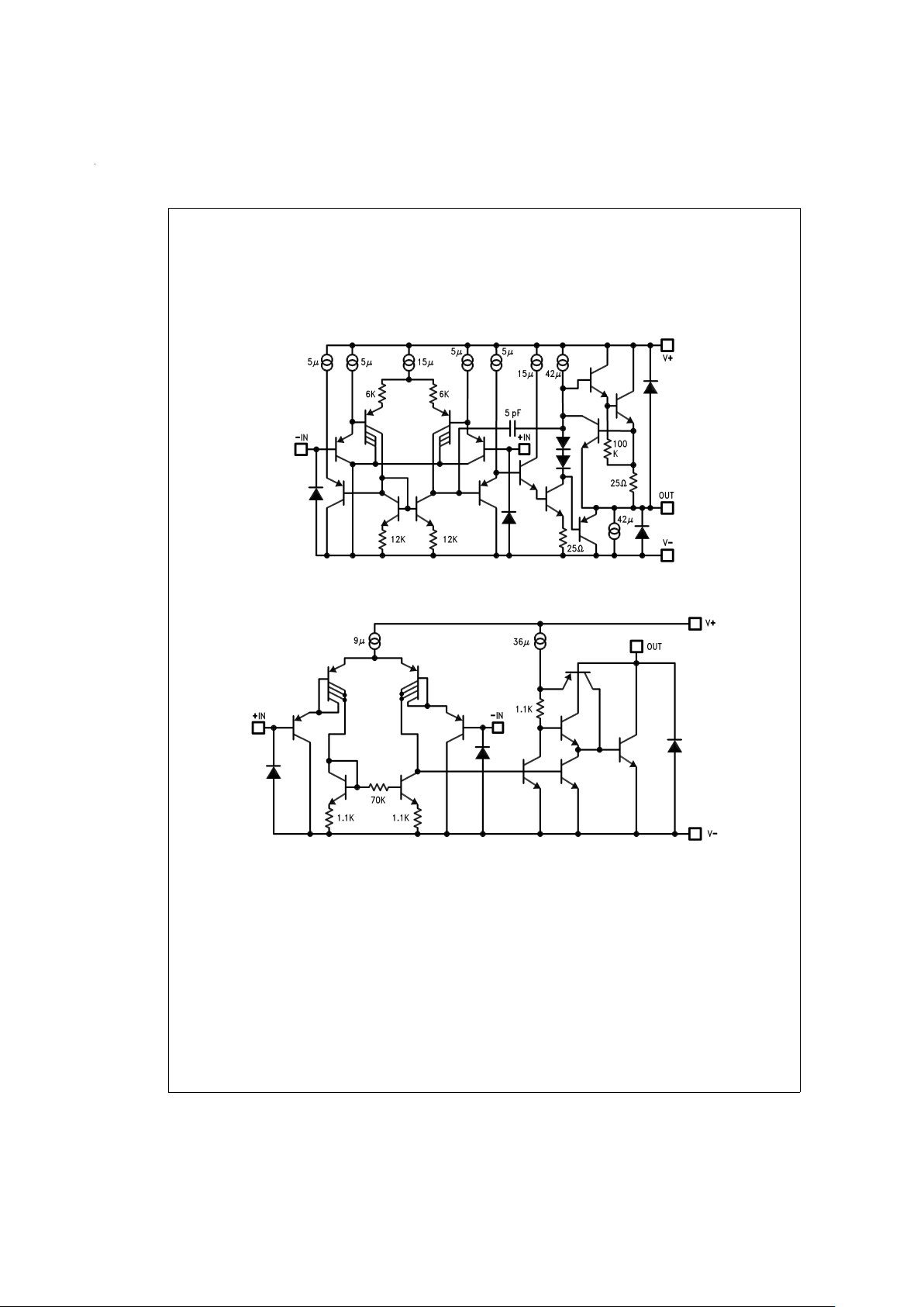
Simplified Schematic Diagrams
Op Amp
DS009226-2
Comparator
DS009226-3
www.national.com 6
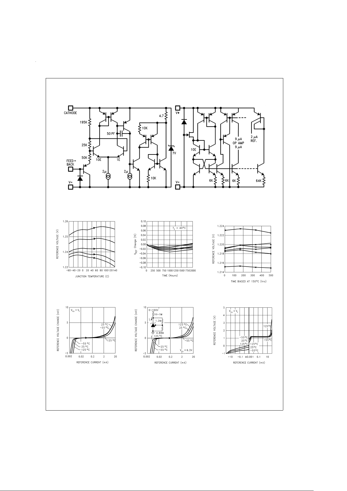
Simplified Schematic Diagrams (Continued)
Typical Performance Characteristics (Reference) T
J
=
25˚C, FEEDBACK pin shorted to V
−
=
0V, unless otherwise noted
Reference/Bias
DS009226-4
Reference Voltage vs Temp.
DS009226-49
Reference Voltage Drift
DS009226-50
Accelerated Reference
Voltage Drift vs Time
DS009226-51
Reference Voltage vs
Current and Temperature
DS009226-52
Reference Voltage vs
Current and Temperature
DS009226-53
Reference Voltage vs
Reference Current
DS009226-54
www.national.com7
 Loading...