

LM6132 Dual/LM6134 Quad
Low Power 10 MHz Rail-to-Rail I/O Operational
Amplifiers
LM6132 Dual and LM6134 Quad, Low Power 10 MHz Rail-to-Rail I/O Operational Amplifiers
April 2000
General Description
The LM6132/34 provides new levels of speed vs power performance in applications where low voltage supplies or
power limitations previously made compromise necessary.
With only 360 µA/amp supply current, the 10 MHz
gain-bandwidth ofthis device supports new portable applications where higher power devices unacceptably drain battery
life.
The LM6132/34 can be driven by voltages that exceed both
power supply rails, thus eliminating concerns over exceeding
the common-mode voltage range. The rail-to-rail output
swing capability provides the maximum possible dynamic
range at the output. This is particularly important when operating on low supply voltages. The LM6132/34 can also drive
large capacitive loads without oscillating.
Operating on supplies from 2.7V to over 24V,the LM6132/34
is excellent for a very wide range of applications, from battery operated systems with large bandwidth requirements to
high speed instrumentation.
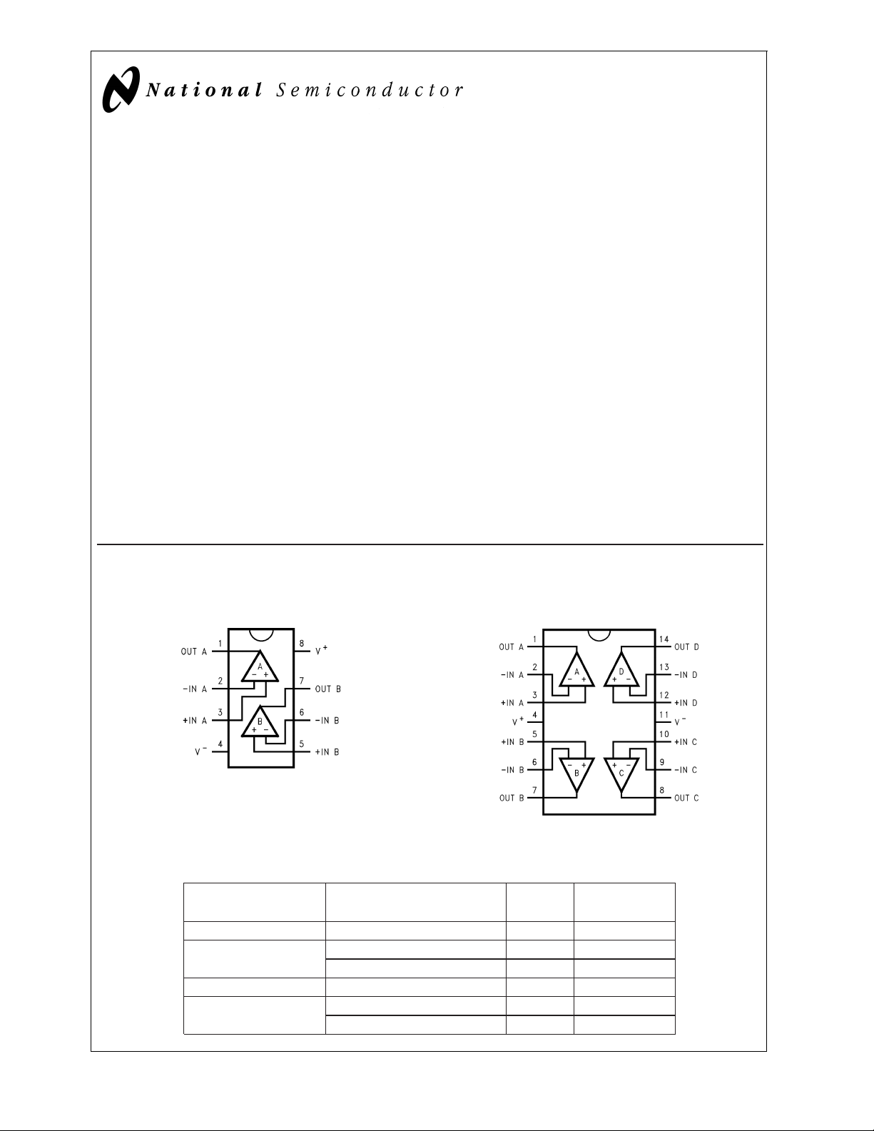
Connection Diagrams
8-Pin DIP/SO
Features
(For 5V Supply, Typ Unless Noted)
n Rail-to-Rail input CMVR −0.25V to 5.25V
n Rail-to-Rail output swing 0.01V to 4.99V
n High gain-bandwidth, 10 MHz at 20 kHz
n Slew rate 12 V/µs
n Low supply current 360 µA/Amp
n Wide supply range 2.7V to over 24V
n CMRR 100 dB
n Gain 100 dB with R
n PSRR 82 dB
L
= 10k
Applications
n Battery operated instrumentation
n Instrumentation Amplifiers
n Portable scanners
n Wireless communications
n Flat panel display driver
14-Pin DIP/SO
DS012349-1
Top View
DS012349-2
Top View
Ordering Information
Package Temperature Range NSC Transport
Industrial, −40˚C to +85˚C Drawing Media
8-Pin Molded DIP LM6132AIN, LM6132BIN N08E Rails
8-Pin Small Outline LM6132AIM, LM6132BIM M08A Rails
LM6132AIMX, LM6132BIMX M08A Tape and Reel
14-Pin Molded DIP LM6134AIN, LM6134BIN N14A Rails
14-Pin Small Outline LM6134AIM, LM6134BIM M14A Rails
LM6134AIMX, LM6134BIMX M14A Tape and Reel
© 2000 National Semiconductor Corporation DS012349 www.national.com
Absolute Maximum Ratings (Note 1)
Junction Temperature (Note 4) 150˚C
If Military/Aerospace specified devices are required,
please contact the National Semiconductor Sales Office/
Distributors for availability and specifications.
ESD Tolerance (Note 2) 2500V
LM6132/LM6134
Differential Input Voltage 15V
Voltage at Input/Output Pin (V
+–V−
Supply Voltage (V
) 35V
+
)+0.3V, (V−)−0.3V
Current at Input Pin
Current at Output Pin (Note 3)
Current at Power Supply Pin 50 mA
±
10 mA
±
25 mA
Operating Ratings(Note 1)
Supply Voltage 1.8V ≤ V
Junction Temperature Range
LM6132, LM6134 −40˚C ≤ T
Thermal resistance (θ
N Package, 8-pin Molded DIP 115˚C/W
M Package, 8-pin Surface Mount 193˚C/W
N Package, 14-pin Molded DIP 81˚C/W
M Package, 14-pin Surface Mount 126˚C/W
)
JA
Lead Temp. (soldering, 10 sec.) 260˚C
Storage Temperature Range −65˚C to +150˚C
5.0V DC Electrical Characteristics
Unless otherwise specified, all limits guaranteed for TJ= 25˚C, V+= 5.0V, V−= 0V, VCM=VO=V+/2 and R
Boldface limits apply at the temperature extremes
LM6134AI LM6134BI
Symbol Parameter Conditions
V
OS
TCV
I
B
I
OS
R
IN
CMRR Common Mode Rejection Ratio 0V ≤ V
PSRR Power Supply Rejection Ratio
V
CM
Input Offset Voltage 0.25 2
Input Offset Voltage Average Drift 5 µV/C
OS
Input Bias Current 0V ≤ VCM≤ 5V 110 140
Input Offset Current 3.4 30
Input Resistance, CM 104 MΩ
≤ 4V 100 75
CM
0V ≤ V
±
2.5V ≤ VS≤±12V 82 78
≤ 5V 80 60
CM
Input Common-Mode Voltage
Range
A
V
V
O
Large Signal Voltage Gain RL= 10k 100 25
Output Swing 100k Load 4.992 4.98
10k Load 4.952 4.94
5k Load 4.923 4.90
I
SC
Output Short Circuit Current
Sourcing 4 2
LM6132
Sinking 3.5 1.8
Typ
(Note 5)
−0.25 00
5.25 5.0 5.0
0.007 0.017
0.032 0.07
0.051 0.095
LM6132AI LM6132BI
Limit Limit
(Note 6) (Note 6)
4
300
50
70
55
75
8
4.93
0.019
4.85
0.09
4.85
0.12
2
1.8
L
6
8
180
350
30
50
75
70
60
55
78
75
15
6
4.98
4.93
0.017
0.019
4.94
4.85
0.07
0.09
4.90
4.85
0.095
0.12
2
1
1.8
1
>
≤ 24V
S
≤ +85˚C
J
1MΩto VS/2.
Units
mV
max
nA
max
nA
max
dB
min
dB
min
V
V/mV
min
V
min
V
max
V
min
V
max
V
min
V
max
mA
min
mA
min
www.national.com 2
5.0V DC Electrical Characteristics (Continued)
Unless otherwise specified, all limits guaranteed for TJ= 25˚C, V+= 5.0V, V−= 0V, VCM=VO=V+/2 and R
Boldface limits apply at the temperature extremes
LM6134AI LM6134BI
Symbol Parameter Conditions
Typ
(Note 5)
LM6132AI LM6132BI
Limit Limit
(Note 6) (Note 6)
I
SC
Output Short Circuit Current
LM6134
Sourcing 3 2
1.6
Sinking 3.5 1.8
1.3
I
S
Supply Current Per Amplifier
360
400
450
>
1MΩto VS/2.
L
2
1
1.8
1
400
450
Units
mA
min
mA
min
µA
max
5.0V AC Electrical Characteristics
Unless otherwise specified, all limits guaranteed for TJ= 25˚C, V+= 5.0V, V−= 0V, VCM=VO=V+/2 and R
Boldface limits apply at the temperature extremes
LM6134AI LM6134BI
Symbol Parameter Conditions
Typ
(Note 5)
LM6132AI LM6132BI
Limit Limit
(Note 6) (Note 6)
±
SR Slew Rate
4V@VS=±6V 14 8 8 V/µs
<
R
1kΩ 77min
S
GBW Gain-Bandwidth Product f = 20 kHz 10 7.4 7.4 MHz
77min
θm Phase Margin R
G
m
e
n
Gain Margin RL= 10k 10 dB
Input Referred Voltage Noise f = 1 kHz 27
= 10k 33 deg
L
>
1MΩto VS/2.
L
Units
LM6132/LM6134
i
n
Input Referred Current Noise f = 1 kHz 0.18
www.national.com3
2.7V DC Electrical Characteristics
Unless otherwise specified, all limits guaranteed for TJ= 25˚C, V+= 2.7V, V−= 0V, VCM=VO=V+/2 and R
Boldface limits apply at the temperature extreme
LM6134AI LM6134BI
Symbol Parameter Conditions
LM6132/LM6134
V
OS
I
B
I
OS
R
IN
Input Offset Voltage 0.12 2 6 mV
Input Bias Current 0V ≤ VCM≤ 2.7V 90 nA
Input Offset Current 2.8 nA
Input Resistance 134 MΩ
CMRR Common Mode 0V ≤ V
Rejection Ratio
PSRR Power Supply
±
1.35V ≤ VS≤±12V 80 dB
Rejection Ratio
V
CM
Input Common-Mode 2.7 2.7 V
Voltage Range 0 0
A
V
Large Signal RL= 10k 100 V/mV
Voltage Gain
V
O
I
S
Output Swing RL= 100k 0.03 0.08 0.08 V
Supply Current Per Amplifier 330 µA
Typ
(Note 5)
≤ 2.7V 82 dB
CM
2.66 2.65 2.65 V
LM6132AI LM6132BI
Limit Limit
(Note 6) (Note 6)
812max
0.112 0.112 max
2.25 2.25 min
>
1MΩto VS/2.
L
Units
2.7V AC Electrical Characteristics
Unless otherwise specified, all limits guaranteed for TJ= 25˚C, V+= 2.7V, V−= 0V, VCM=VO=V+/2 and R
LM6134AI LM6134BI
Symbol Parameter Conditions
GBW Gain-Bandwidth Product R
θ
m
G
m
Phase Margin RL= 10k 23 deg
Gain Margin 12 dB
= 10k, f = 20 kHz 7 MHz
L
Typ
(Note 5)
LM6132AI LM6132BI
Limit Limit
(Note 6) (Note 6)
>
1MΩto VS/2.
L
Units
www.national.com 4
24V DC Electrical Characteristics
Unless otherwise specified, all limits guaranteed for TJ= 25˚C, V+= 24V, V−= 0V, VCM=VO=V+/2 and R
Boldface limits apply at the temperature extreme
LM6134AI LM6134BI
Symbol Parameter Conditions
V
OS
I
B
I
OS
R
IN
CMRR Common Mode 0V ≤ V
Input Offset Voltage 1.7 3 7 mV
Input Bias Current 0V ≤ VCM≤ 24V 125 nA
Input Offset Current 4.8 nA
Input Resistance 210 MΩ
≤ 24V 80 dB
CM
Rejection Ratio
PSRR Power Supply 2.7V ≤ V
≤ 24V 82 dB
S
Rejection Ratio
V
CM
Input Common-Mode −0.25 0 0 V min
Voltage Range 24.25 24 24 V max
A
V
Large Signal RL= 10k 102 V/mV
Voltage Gain
V
O
I
S
Output Swing RL= 10k 0.075 0.15 0.15 V
Supply Current Per Amplifier 390 450 450 µA
Typ
(Note 5)
23.86 23.8 23.8 V
LM6132AI LM6132BI
Limit Limit
(Note 6) (Note 6)
59max
490 490 max
>
1MΩto VS/2.
L
LM6132/LM6134
Units
max
min
24V AC Electrical Characteristics
Unless otherwise specified, all limits guaranteed for TJ= 25˚C, V+= 24V, V−= 0V, VCM=VO=V+/2 and R
LM6134AI LM6134BI
Symbol Parameter Conditions
Typ
(Note 5)
LM6132AI LM6132BI
Limit Limit
(Note 6) (Note 6)
GBW Gain-Bandwidth Product R
θ
m
G
m
THD +
Phase Margin RL= 10k 23 deg
Gain Margin RL= 10k 12 dB
Total Harmonic A
N
= 10k, f = 20 kHz 11 MHz
L
= +1, VO= 20V
V
P-P
0.0015 %
Distortion and Noise f = 10 kHz
Note 1: Absolute Maximum Ratings indicate limits beyond which damage to the device may occur. Operating Ratings indicate conditions for which the device is intended to be functional, but specific performance is not guaranteed. For guaranteed specifications and the test conditions, see the Electrical characteristics.
Note 2: Human body model, 1.5 kΩ in series with 100 pF.
Note 3: Applies to both single-supply and split-supply operation. Continuous short circuit operation at elevated ambient temperature can result in exceeding the
maximum allowed junction temperature of 150˚C.
Note 4: The maximum power dissipation isafunctionofT
−TA)/θJA. All numbers apply for packages soldered directly into a PC board.
Note 5: Typical Values represent the most likely parametric norm.
Note 6: All limits are guaranteed by testing or statistical analysis.
, θJA, and TA. The maximum allowable power dissipation at any ambient temperature is PD=(T
J(max)
>
1MΩto VS/2.
L
Units
J(max)
www.national.com5
 Loading...