

NSC LM4878IBPX, LM4878IBP Datasheet
October 2002
LM4878
1 Watt Audio Power Amplifier in micro SMD package
with Shutdown Logic Low
LM4878 1 Watt Audio Power Amplifier in micro SMD package with Shutdown Logic Low
General Description
The LM4878 is a bridge-connected audio power amplifier
capable of delivering1Wofcontinuous average power to an
8Ω load with less than .2% (THD) from a 5V power supply.
Boomer audio power amplifiers were designed specifically to
provide high quality output power with a minimal amount of
external components. Since the LM4878 does not require
output coupling capacitors or bootstrap capacitors. It is optimally suited for low-power portable applications.
The LM4878 features an externally controlled, low-power
consumption shutdown mode, as well as an internal thermal
shutdown protection mechanism.
The unity-gain stable LM4878 can be configured by external
gain-setting resistors.
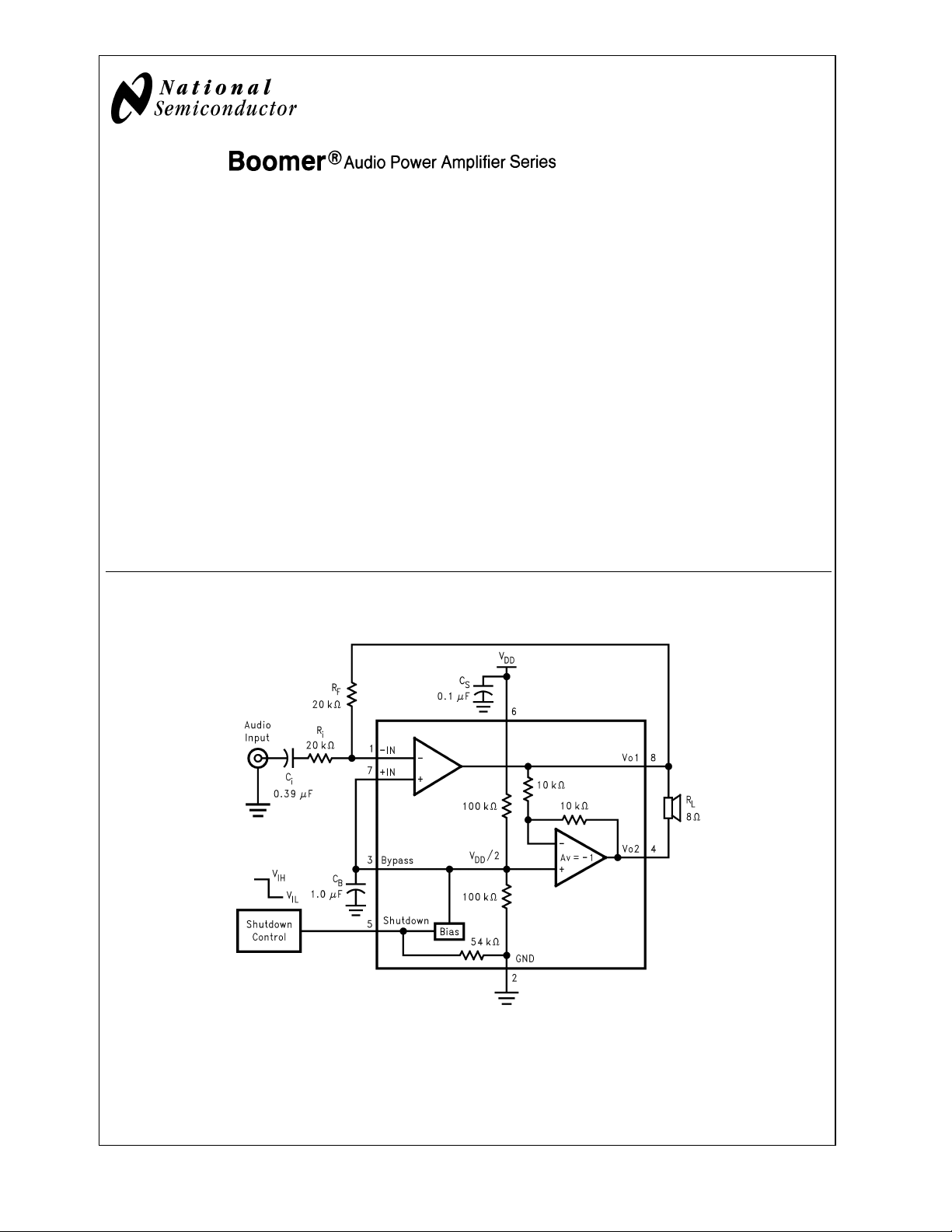
Typical Application
Key Specifications
j
Power Output at 0.2% THD 1 W (typ)
j
Shutdown Current 0.01 µA (typ)
Features
n Internal pulldown resistor on shutdown.
n micro SMD package (see App. note AN-1112)
n 5V - 2V operation
n No output coupling capacitors or bootstrap capacitors.
n Unity-gain stable
n External gain configuration capability
Applications
n Cellular Phones
n Portable Computers
n Low Voltage Audio Systems
10136001
FIGURE 1. Typical Audio Amplifier Application Circuit
Boomer®is a registered trademark of National Semiconductor Corporation.
© 2002 National Semiconductor Corporation DS101360 www.national.com
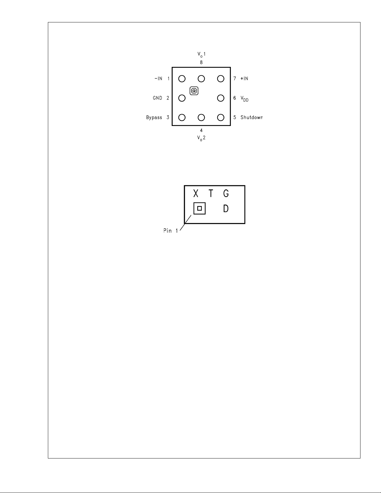
Connection Diagrams
LM4878
8 Bump micro SMD
Top View
10136023
Order Number LM4878IBP, LM4878IBPX
See NS Package Number BPA08B6B
micro SMD Marking
Top View
10136036
X - Date Code
T - Die Traceability
G - Boomer Family
D - LM4878IBP
www.national.com 2
LM4878
Absolute Maximum Ratings (Note 2)
If Military/Aerospace specified devices are required,
please contact the National Semiconductor Sales Office/
Soldering Information
See AN-1112 ’Micro-SMD Wafers Level Chip Scale
Package’.
Distributors for availability and specifications.
Supply Voltage 6.0V
Storage Temperature −65˚C to +150˚C
Input Voltage −0.3V to V
DD
+0.3V
Power Dissipation (Note 3) Internally Limited
Operating Ratings
Temperature Range
ESD Susceptibility (Note 4) 2500V
ESD Susceptibility (Note 5) 250V
Supply Voltage 2.0V ≤ V
Junction Temperature 150˚C
Electrical Characteristics VDD=5V (Notes 1, 2, 9)
The following specifications apply for V
Symbol Parameter Conditions
V
DD
I
DD
I
SD
V
OS
P
o
Supply Voltage 2.0 V (min)
Quiescent Power Supply Current VIN= 0V, Io= 0A 5.3 7 mA (max)
Shutdown Current V
Output Offset Voltage VIN= 0V 5 50 mV (max)
Output Power THD = 0.2% (max);f=1kHz 1 W
THD+N Total Harmonic Distortion+Noise P
PSRR Power Supply Rejection Ratio V
= 5V and 8Ω Load unless otherwise specified. Limits apply for TA= 25˚C.
DD
= 0V 0.01 2 µA (max)
PIN5
= 0.25 Wrms; AVD=2;20Hz≤
o
f ≤ 20 kHz
= 4.9V to 5.1V 65 dB
DD
T
MIN
≤ TA≤ T
MAX
−40˚C ≤ TA≤ 85˚C
LM4878
Typical Limit
(Note 6) (Note 7)
5.5 V (max)
0.1 %
≤ 5.5V
DD
Units
(Limits)
Electrical Characteristics VDD= 3.3V (Notes 1, 2, 9)
The following specifications apply for V
Symbol Parameter Conditions
V
DD
I
DD
I
SD
V
OS
P
o
Supply Voltage 2.0 V (min)
Quiescent Power Supply Current VIN= 0V, Io= 0A 4 mA (max)
Shutdown Current V
Output Offset Voltage VIN= 0V 5 mV (max)
Output Power THD = 1% (max);f=1kHz .5 .45 W
THD+N Total Harmonic Distortion+Noise P
PSRR Power Supply Rejection Ratio V
= 3.3V and 8Ω Load unless otherwise specified. Limits apply for TA= 25˚C.
DD
= 0V 0.01 µA (max)
PIN5
= 0.25 Wrms; AVD=2;20Hz≤
o
f ≤ 20 kHz
= 3.2V to 3.4V 65 dB
DD
Electrical Characteristics VDD= 2.6V (Notes 1, 2, 8, 9)
The following specifications apply for V
Symbol Parameter Conditions
V
DD
I
DD
I
SD
Supply Voltage 2.0 V (min)
Quiescent Power Supply Current VIN= 0V, Io= 0A 3.4 mA (max)
Shutdown Current V
= 2.6V and 8Ω Load unless otherwise specified. Limits apply for TA= 25˚C.
DD
= 0V 0.01 µA (max)
PIN5
LM4878
Typical Limit
(Note 6) (Note 7)
5.5 V (max)
0.15 %
LM4878
Typical Limit
(Note 6) (Note 7)
5.5 V (max)
Units
(Limits)
Units
(Limits)
www.national.com3
Electrical Characteristics VDD= 2.6V (Notes 1, 2, 8, 9)
The following specifications apply for V
LM4878
25˚C. (Continued)
= 2.6V and 8Ω Load unless otherwise specified. Limits apply for TA=
DD
Symbol Parameter Conditions
V
OS
P
0
Output Offset Voltage VIN= 0V 5 mV (max)
Output Power ( 8Ω )
Output Power ( 4Ω )
THD = 0.3% (max);f=1kHzTHD
= 0.5% (max);f=1kHz
THD+N Total Harmonic Distortion+Noise Po= 0.25 Wrms; AVD=2;20Hz≤
LM4878
Typical Limit
(Note 6) (Note 7)
0.25
0.5
0.25 %
Units
(Limits)
f ≤ 20 kHz
PSRR Power Supply Rejection Ratio V
Note 1: All voltages are measured with respect to the ground pin, unless otherwise specified.
Note 2: Absolute Maximum Ratings indicate limits beyond which damage to the device may occur. Operating Ratings indicate conditions for which the device is
functional, but do not guarantee specific performance limits. Electrical Characteristics state DC and AC electrical specifications under particular test conditions which
guarantee specific performance limits. This assumes that the device is within the Operating Ratings. Specifications are not guaranteed for parameters where no limit
is given, however, the typical value is a good indication of device performance.
Note 3: The maximum power dissipation must be derated at elevated temperatures and is dictated by T
allowable power dissipation is P
The typical junction-to-ambient thermal resistance is 150˚C/W.
Note 4: Human body model, 100 pF discharged through a 1.5 kΩ resistor.
Note 5: Machine Model, 220 pF–240 pF discharged through all pins.
Note 6: Typicals are measured at 25˚C and represent the parametric norm.
Note 7: Limits are guaranteed to National’s AOQL (Average Outgoing Quality Level).
Note 8: Low Voltage Circuit - See Fig. 4
Note 9: Shutdown current is measured in a Normal Room Environment. Exposure to direct sunlight will increase I
DMAX
=(T
)/θJAor the number given in Absolute Maximum Ratings, whichever is lower. For the LM4878, T
JMAX–TA
= 2.5V to 2.7V 65 dB
DD
, θJA, and the ambient temperature TA. The maximum
JMAX
by a maximum of 2µA.
SD
JMAX
= 150˚C.
Electrical Characteristics VDD= 5/3.3/2.6V Shutdown Input
W
W
Symbol Parameter Conditions
V
IH
V
IL
Shutdown Input Voltage High 1.2 V(min)
Shutdown Input Voltage Low 0.4 V(max)
External Components Description
(Figure 1)
Components Functional Description
1. R
2. C
3. R
4. C
5. C
Inverting input resistance which sets the closed-loop gain in conjunction with Rf. This resistor also forms a
i
high pass filter with C
Input coupling capacitor which blocks the DC voltage at the amplifiers input terminals. Also creates a
i
highpass filter with R
for an explanation of how to determine the value of C
Feedback resistance which sets the closed-loop gain in conjunction with Ri.
f
Supply bypass capacitor which provides power supply filtering. Refer to the Power Supply Bypassing
S
at fC= 1/(2π RiCi).
i
at fc= 1/(2π RiCi). Refer to the section, Proper Selection of External Components,
i
.
i
section for information concerning proper placement and selection of the supply bypass capacitor.
Bypass pin capacitor which provides half-supply filtering. Refer to the section, Proper Selection of External
B
Components, for information concerning proper placement and selection of C
LM4878
Typical Limit
.
B
Units
(Limits)
www.national.com 4
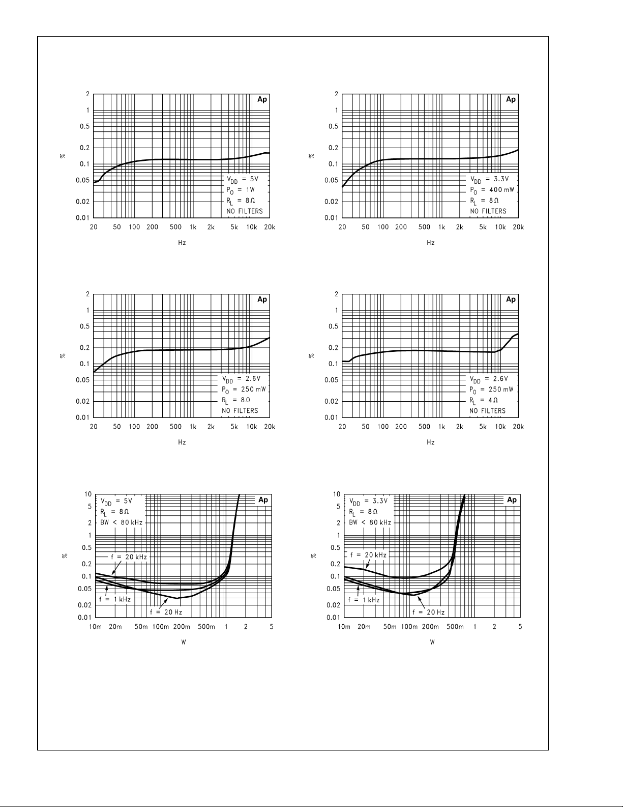
Typical Performance Characteristics
LM4878
THD+N vs Frequency
at 5V and 8Ω
THD+N vs Frequency
at 2.6V and 8Ω
THD+N vs Frequency
at 3.3V and 8Ω
10136003 10136006
THD+N vs Frequency
at 2.6V and 4Ω
THD+N vs Output Power
@
VDD=5V
10136005 10136004
THD+N vs Output Power
@
VDD= 3.3V
10136007 10136008
www.national.com5
 Loading...