

NSC LM4874MH Datasheet
LM4874
2.1W Differential Input, BTL Output Stereo Audio
Amplifier with Selectable Gain and Shutdown
August 2002
LM4874 Boomer 2.1W Differential Input, BTL Output Stereo Audio Amplifier with Selectable Gain
and Shutdown
General Description
The LM4874 features differential stereo inputs, BTL (bridgetied load) outputs, and four externally selectable fixed gains.
Operating on a single 5V supply, the LM4874 delivers 1.2W,
1.9W, or 2.1W (typ) of output power to an 8Ω,4Ω,or3Ω BTL
load (Note 1), respectively, with less than 1% THD+N. The
LM4874’s gain is selected using two digital inputs. The nominal gain values are 6dB, 10dB, 15.6dB, and 21.6dB.
The LM4874 is designed for notebook and other handheld
portable applications. It delivers high quality output power
from a surface-mount package and requires few external
components.
Other features include an active-low micropower shutdown
mode input and thermal shutdown protection.
Key Specifications
j
BTL output power
R
=3Ω,VDD= 5.0V, and THD+N = 1% 2.1W (typ)
L
j
BTL output power
R
=4Ω,VDD= 5.0V, and THD+N = 1% 1.9W (typ)
L
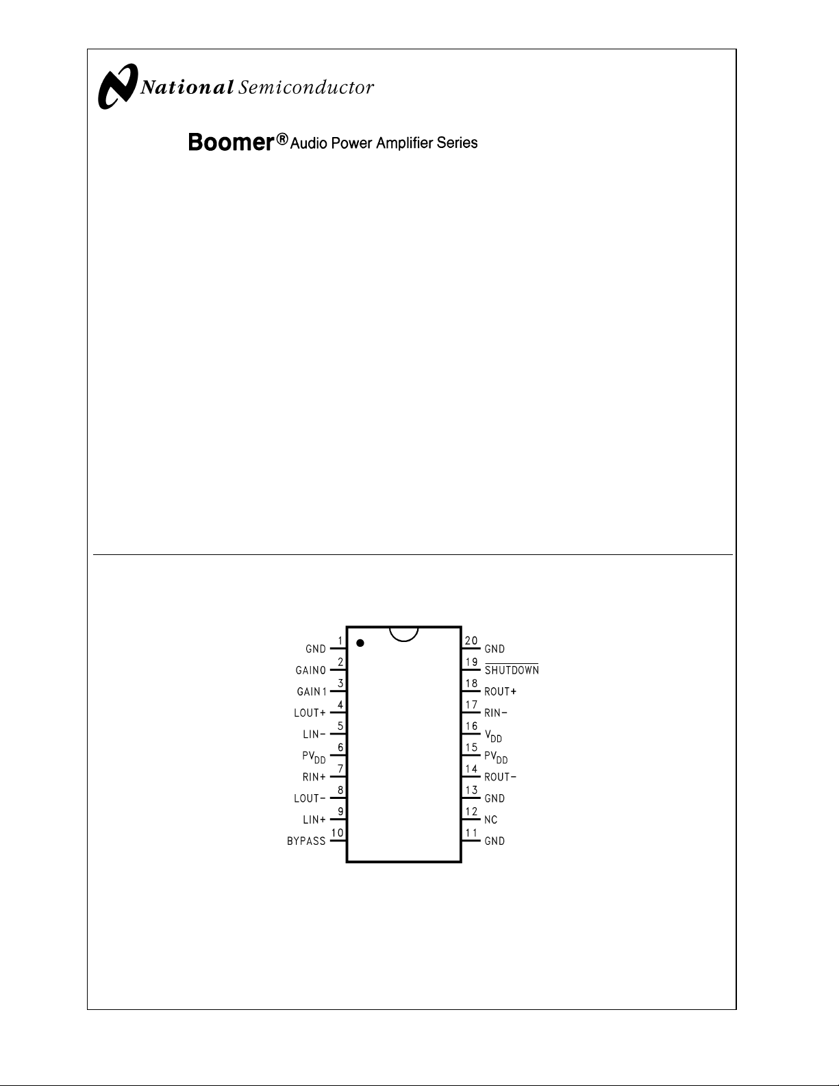
Connection Diagram
Top View
j
BTL output power
R
=8Ω,VDD= 5.0V, and THD+N = 1% 1.2W (typ)
L
j
Micropower shutdown current 0.1µA (typ)
j
PSRR (@1kHz, VDD= 5V, (Fig.1)) 62dB (typ)
Features
n Fully differential input and output
n Internal gain set: 6dB, 10dB, 15.6dB, and 21.6dB
n Improved ’click and pop’ suppression
n Thermal shutdown protection circuit
n Ultra low current micropower shutdown mode
n 3.0V to 5.5V operation
n Available in space-saving exposed-DAP TSSOP
package
Applications
n Notebook computers
n PDAs
n Portable electronic devices
Order Number LM4874MH
See NS Package Number MXA20A for Exposed-DAP TSSOP
Boomer®is a registered trademark of National Semiconductor Corporation.
© 2002 National Semiconductor Corporation DS200469 www.national.com
20046902
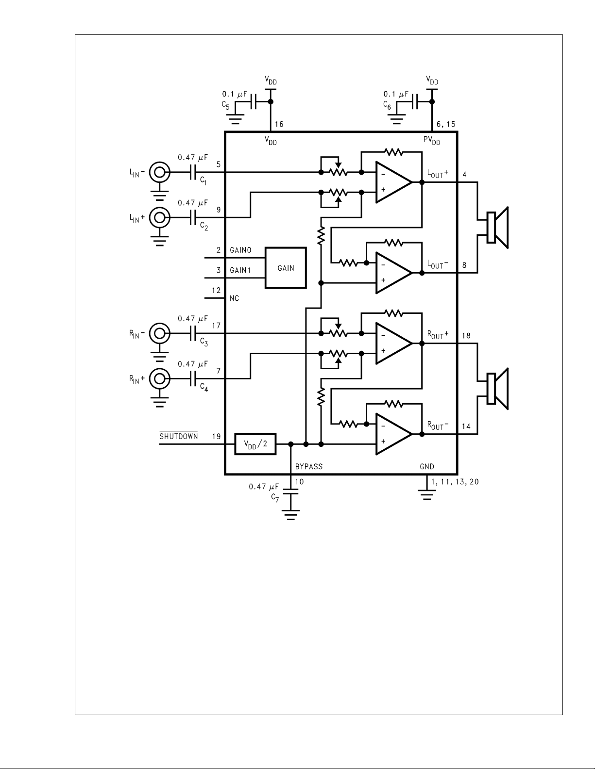
Typical Application
LM4874
FIGURE 1. Typical Audio Amplifier Application Circuit
www.national.com 2
20046901
LM4874
Absolute Maximum Ratings (Notes 2,
3)
If Military/Aerospace specified devices are required,
please contact the National Semiconductor Sales Office/
Distributors for availability and specifications.
Supply Voltage 6.0V
Storage Temperature -65˚C to + 150˚C
Input Voltage −0.3V to V
Power Dissipation (Note 4) Internally Limited
ESD Susceptibility (Note 5) 2000V
ESD Susceptibility (Note 6) 200V
Junction Temperature 150˚C
Soldering Information
DD
+ 0.3V
Infrared (15 sec.) 220˚C
See AN-450 “Surface Mounting and their Effects on
Product Reliability” for other methods of soldering surface
mount devices.
Thermal Resistance
θ
(typ) MXA20A 2˚C/W
JC
θ
(typ) MXA20A 41˚C/W (Note 7)
JA
Operating Ratings
Temperature Range
≤ TA≤T
T
MIN
MAX
Supply Voltage 3.0 V ≤ V
−40˚C ≤ TA ≤ 85˚C
≤ 5.5V
DD
Small Outline Package
Vapor Phase (60 sec.) 215˚C
Electrical Characteristics for LM4874 (Notes 2, 8)
The following specifications applies to the LM4874 when used in the circuit shown in Figure 1 and operating with VDD=5Vand
= 6dB, unless otherwise specified. Limits apply for TA= 25˚C.
A
V
LM4874
Symbol Parameter Conditions
V
DD
Supply Voltage 3.0
Typical
(Note 8)
Limit
(Notes 9,
10)
5.5
I
DD
I
SD
V
OS
Quiescent Power Supply Current VIN= 0V, IO= 0A, RL=
Shutdown Current V
Output Offset Voltage 7 50 mV (max)
PSRR Output Supply Rejection Ratio V
P
O
Output Power (Note 11) THD+N = 1% (max), f = 1kHz (Note12)
shutdown
DD
= GND 0.1 1.0 µA (max)
= 5V, V
sinewave, C
=8Ω
R
L
=3Ω
R
L
=4Ω
R
L
=8Ω
R
L
RIPPLE
BYPASS
∞
= 200mV
= 0.47µF,
P-P
9.0 12.0 mA (max)
62 dB
2.1
1.9
1.2 1.0
THD+N = 10% (max), f = 1kHz
(Note12)
=3Ω
R
L
=4Ω
R
L
=8Ω
R
L
2.6
2.6
1.5
THD+N Total Harmonic Distortion + Noise 20Hz ≤ f ≤ 20kHz
=4Ω,PO=2W
R
L
=8Ω,PO=1W
R
L
S/N Signal-to-Noise Ratio f = 1kHz, C
= 1.1W, RL=8Ω
P
O
R
IN
Note 1: An LM4874MH that has been properly mounted to a circuit board with a copper heatsink area of at least 2in2will deliver 1.9W into 4Ω or 2.1W into 3Ω.
Note 2: All voltages are measured with respect to the GND pin unless other wise specified.
Note 3: Absolute Maximum Ratings indicate limits beyond which damage to the device may occur. Operating Ratings indicate conditions for which the device is
functional but do not guarantee specific performance limits. Electrical Characteristics state DC and AC electrical specifications under particular test conditions that
guarantee specific performance limits. This assumes that the device is within the Operating Ratings. Specifications are not guaranteed for parameters where no limit
is given, however, the typical value is a good indication of device performance.
Note 4: The maximum power dissipation must be derated at elevated temperatures and is dictated by TJMAX, θ
allowable power dissipation is P
currents for more information.
Note 5: Human body model, 100 pF discharged through a 1.5 kΩ resistor.
Input Resistance Pins 5, 7, 9, and 17 See Table 1.
DMAX
=(T
JMAX-TA/θJA
or the number given in Absolute Maximum Ratings, whichever is lower. For the LM4874, see power derating
BYPASS
= 0.47µF,
JA
0.3
0.3
97 dB
, and the ambient temperature, TA. The maximum
Units
(Limits)
V (min)
V (max)
W
W
W (min)
W
W
W
%
%
www.national.com3
Electrical Characteristics for LM4874 (Notes 2, 8) (Continued)
Note 6: Machine Model, 220pF-240pF discharged through all pins.
LM4874
Note 7: The given θ
driving 4Ω loads from a 5V supply, the LM4874MH must be mounted to the circuit board and its exposed-DAP soldered to an exposed 2in
Note 8: Typicals are measured at 25˚C and represent the parametric norm.
Note 9: Limits are guaranteed to National’s AOQL (Average Outgoing Quality Level).
Note 10: Datasheet minimum and maximum specification limits are guaranteed by design, test, or statistical analysis.
Note 11: Output power is measured at the amplifier’s package pins.
Note 12: When driving 3Ω or 4Ω loads and operating on a 5V supply, the LM4874MH must be mounted to a circuit board that has a minimum of 2in
uninterrupted copper area connected to the MH package’s exposed DAP.
is for an LM4874 packaged in an MXA20A with the exposed-DAP soldered to an exposed 2in2area of 1oz printed circuit board copper. When
JA
External Components Description
See Figure 1.
Components Functional Description
1. C
2. C
The input coupling capacitor blocks DC voltage at the amplifier’s inverting input terminals. Ci, along with the
i
LM4874’s variable input resistance R
inverting and noninverting inputs require a C
EXTERNAL COMPONENTS, for an explanation of determining the value of C
The supply bypass capacitor. Refer to the POWER SUPPLY BYPASSING section for information about
S
(See Table 1), creates a highpass filter with fC= 1/(2πRiCi). Both
1
. Refer to the Application Information section, SELECTING
i
.
i
properly placing, and selecting the value of, this capacitor.
3. C
The capacitor, CB, filters the half-supply voltage present on the BYPASS pin. Refer to the Application
B
Information section, SELECTING EXTERNAL COMPONENTS, for information concerning proper placement
and selecting C
’s value.
B
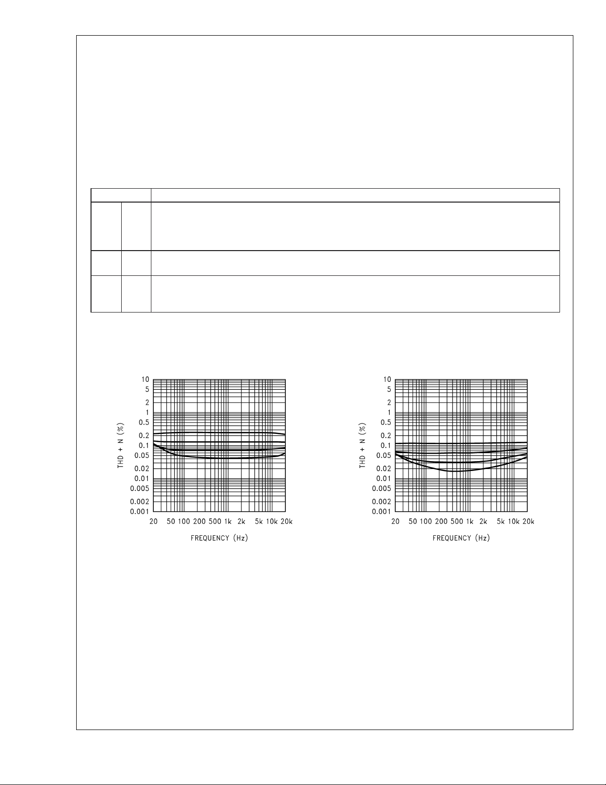
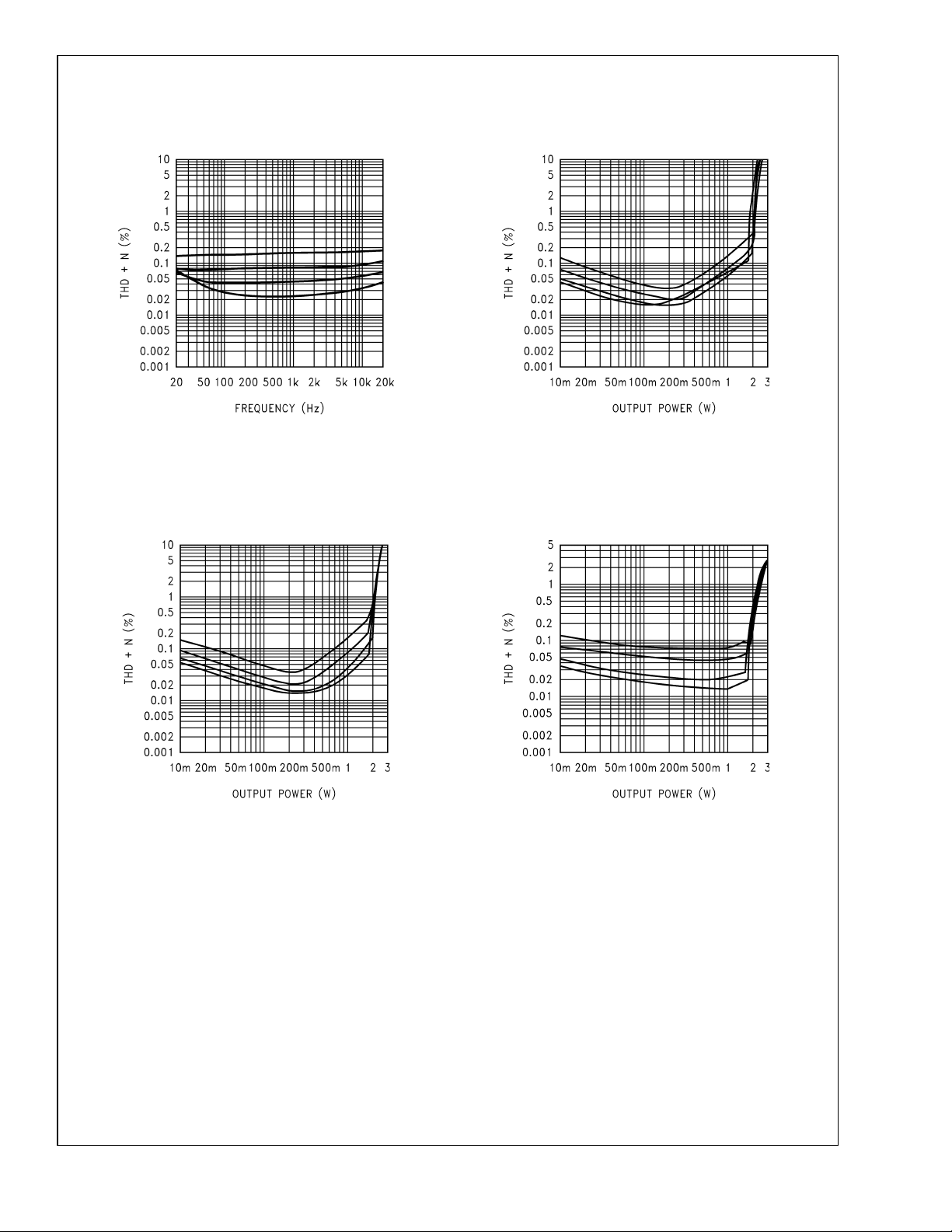
Typical Performance Characteristics MH Specific Characteristics
2
area of 1oz PCB copper.
2
of exposed,
THD vs Frequency THD vs Frequency
VDD= 5V, RL=4Ω,P
= 1000mW,
OUT
at (from top to bottom at 1kHz):
= 21.6dB, AV= 15.6dB,
A
V
= 10dB, AV= 6dB
A
V
20046998
VDD= 5V, RL=8Ω,P
OUT
= 400mW,
at (from top to bottom at 1kHz):
= 21.6dB, AV= 15.6dB,
A
V
= 10dB, AV= 6dB
A
V
20046997
www.national.com 4
Typical Performance Characteristics
MH Specific Characteristics
THD vs Frequency THD vs Frequency
(Continued)
LM4874
VDD= 5V, RL=8Ω,P
OUT
= 400mW,
at (from top to bottom at 1kHz):
= 21.6dB, AV= 15.6dB,
A
V
= 10dB, AV= 6dB
A
V
THD vs Frequency THD vs Frequency
VDD= 5V, RL=3Ω,fIN= 1kHz,
at (from top to bottom at 50mW):
= 21.6dB, AV= 15.6dB,
A
V
= 10dB, AV= 6dB
A
V
20046999
20046944
VDD= 5V, RL=3Ω,fIN= 20Hz,
at (from top to bottom at 50mW):
= 21.6dB, AV= 15.6dB,
A
V
= 10dB, AV= 6dB
A
V
VDD= 5V, RL=3Ω,fIN= 20kHz,
at (from top to bottom at 50mW):
= 21.6dB, AV= 15.6dB,
A
V
= 10dB, AV= 6dB
A
V
20046943
20046945
www.national.com5
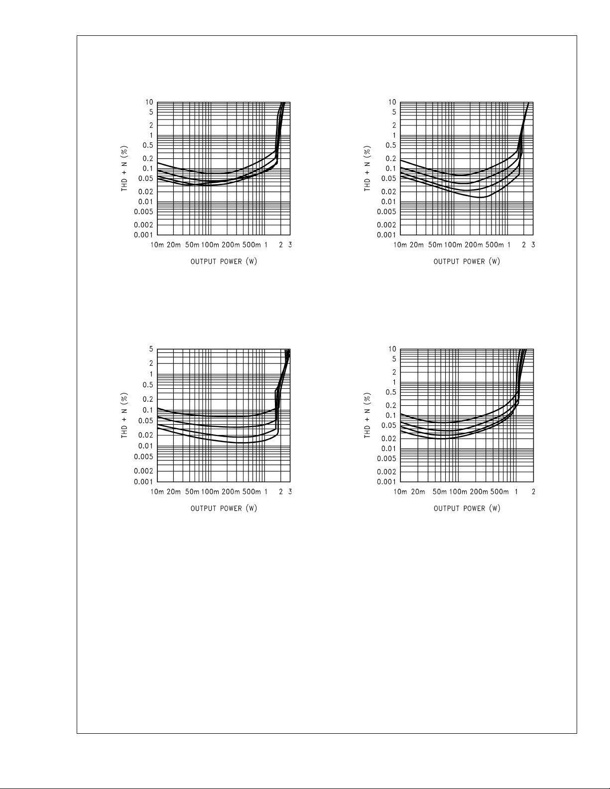
Typical Performance Characteristics
MH Specific Characteristics
LM4874
THD vs Output Power THD vs Output Power
(Continued)
VDD= 5V, RL=4Ω,fIN= 20Hz,
at (from top to bottom at 100mW):
= 21.6dB, AV= 15.6dB,
A
V
= 6dB, AV= 10dB
A
V
200469A0
VDD= 5V, RL=4Ω,fIN= 1kHz,
at (from top to bottom at 200mW):
= 21.6dB, AV= 15.6dB,
A
V
= 10dB, AV= 6dB
A
V
THD vs Output Power THD vs Output Power
VDD= 5V, RL=4Ω,fIN= 20kHz,
at (from top to bottom at 200mW):
= 21.6dB, AV= 15.6dB,
A
V
= 10dB, AV= 6dB
A
V
200469A2
VDD= 5V, RL=8Ω,fIN= 20Hz,
at (from top to bottom at 200mW):
= 21.6dB, AV= 15.6dB,
A
V
= 10dB, AV= 6dB
A
V
200469A1
200469A3
www.national.com 6
Typical Performance Characteristics
MH Specific Characteristics
THD vs Output Power THD vs Output Power
(Continued)
LM4874
VDD= 5V, RL=8Ω,fIN= 1kHz,
at (from top to bottom at 200mW):
= 21.6dB, AV= 15.6dB,
A
V
= 10dB, AV= 6dB
A
V
200469A4
VDD= 5V, RL=8Ω,fIN= 20kHz,
at (from top to bottom at 200mW):
= 21.6dB, AV= 15.6dB,
A
V
= 10dB, AV= 6dB
A
V
Output Power vs Supply Voltage Output Power vs Supply Voltage
RL=4Ω,fIN= 1kHz,
at (from top to bottom at 4V):
THD+N = 10%, THD+N = 1%
200469C3
RL=8Ω,fIN= 1kHz,
at (from top to bottom at 4V):
THD+N = 10%, THD+N = 1%
200469A5
200469C4
www.national.com7
 Loading...