

LM4868
Output-Transient-Free Dual 2.1W Audio Amplifier Plus
No Coupling Capacitor Stereo Headphone Function
General Description
The LM4868 is a dual bridge-connected audio power amplifier which, when connected to a 5V supply, will deliver 2.1W
toa4Ω load (Note 1) or 2.4W to a 3Ω load (Note 2) with less
than 1.0% THD+N. The LM4868 uses advanced, latest generation circuitry to eliminate all traces of clicks and pops
when the supply voltage is first applied. The amplifier has a
headphone-amplifier-select input pin. It is used to switch the
amplifiers from bridge to single-ended mode for driving
headphones. A new circuit topology eliminates headphone
output coupling capacitors (patent pending). A MUX control
pin allows selection between the two sets of stereo input
signals. The MUX control can also be used to select between two different customer-specified closed-loop responses.
Boomer audio power amplifiers are designed specifically to
provide high quality output power from a surface mount
package and require few external components. To simplify
audio system design, the LM4868 combines dual bridge
speaker amplifiers and stereo headphone amplifiers in one
package.
The LM4868 features an externally controlled power-saving
micropower shutdown mode, a stereo headphone amplifier
mode, and thermal shutdown protection.
Note 1: An LM4868LQ or LM4868MTE that has been properly mounted to
a circuit board will deliver 2.1W into 4Ω. The Mux control can also be used to
select two different closed-loop responses. LM4868MT will deliver 1.1W into
8Ω. See the Application Information sections for further information concerning the LM4868LQ and the LM4868MT.
Note 2: An LM4868LQ or LM4868MTE that has been properly mounted to a
circuit board and forced-air cooled will deliver 2.4W into 3Ω.
Key Specifications
n POat 1% THD+N
n LM4868LQ, 3Ω load 2.4W (typ)
n LM4868LQ, 4Ω load 2.1W (typ)
n LM4868MTE, 4Ω 1.9W (typ)
n LM4868MT, 8Ω 1.1W (typ)
n Single-ended mode - THD+N at 75mW into 32Ω 0.5%
(max)
n Shutdown current 0.7µA (typ)
Features
n Advanced “click and pop” suppression circuitry
n Eliminates headphone amplifier output coupling
capacitors (patent pending)
n Stereo headphone amplifier mode
n Input mux control and two separate inputs per channel
n Thermal shutdown protection circuitry
n LLP, TSSOP, and exposed-DAP TSSOP packaging
available
Applications
n Multimedia monitors
n Portable and desktop computers
n Portable audio systems
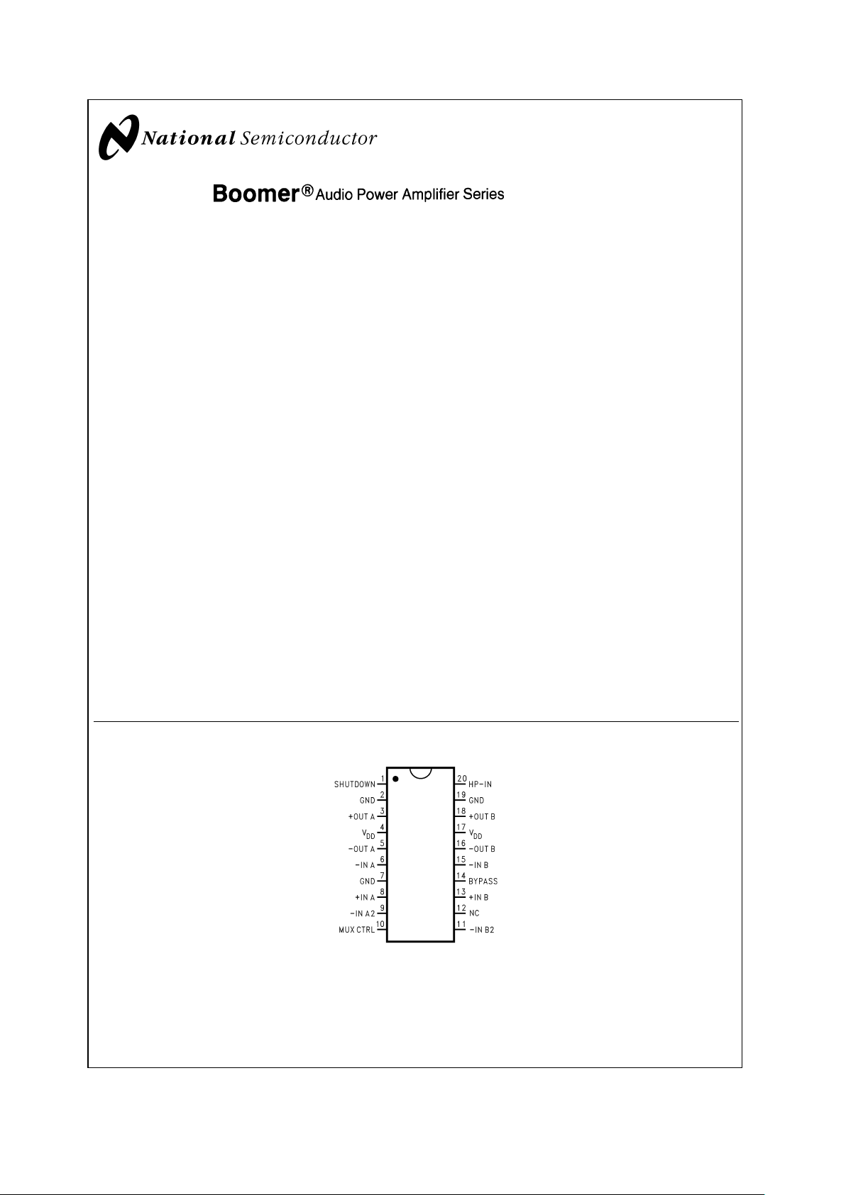
Connection Diagrams
20026758
Top View
Order Number LM4868MT, LM4868MTE
See NS Package Number MTC20 for TSSOP
See NS Package Number MXA20A for Exposed-DAP TSSOP
Boomer®is a registered trademark of National Semiconductor Corporation.
August 2002
LM4868 Output-Transient-Free Dual 2.1W Audio Amplifier Plus No Coupling Capacitor Stereo
Headphone Function
© 2002 National Semiconductor Corporation DS200267 www.national.com
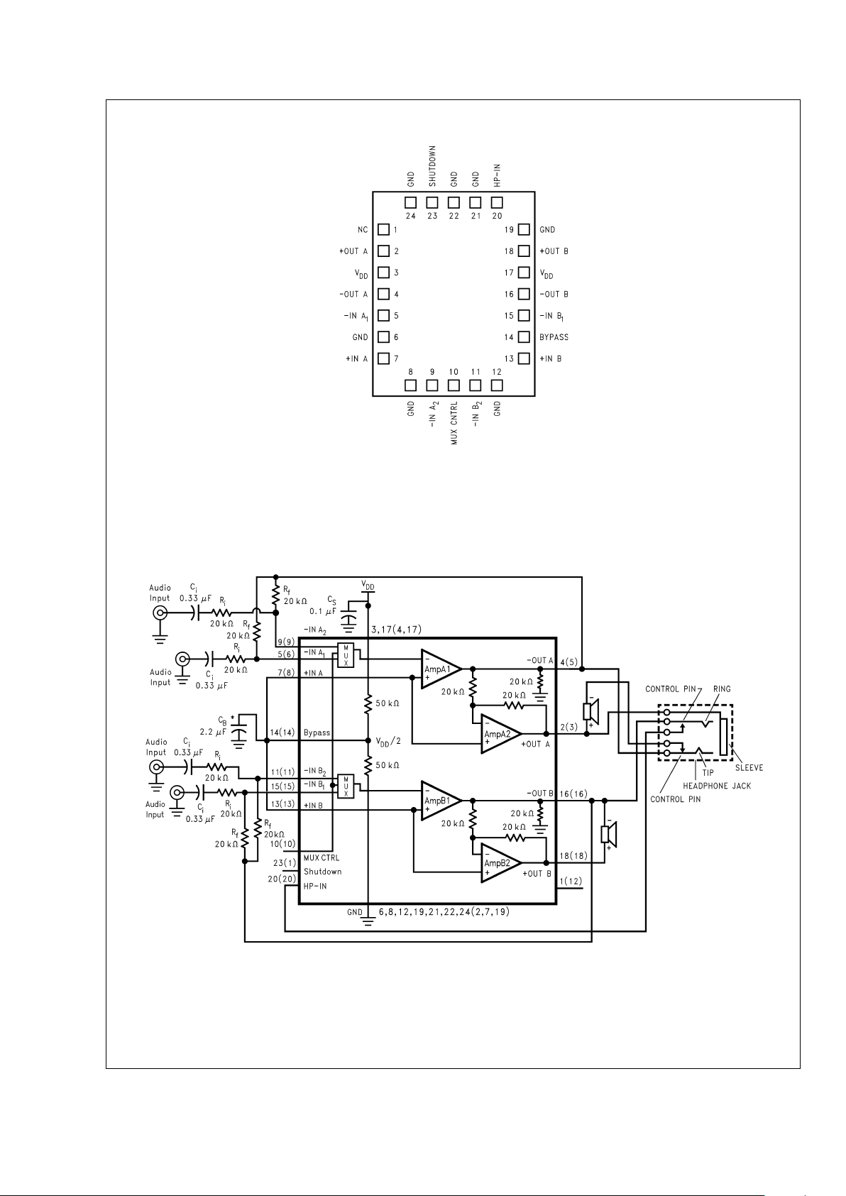
Connection Diagrams (Continued)
20026738
Top View
Order Number LM4868LQ
See NS Package Number LQA24A for Exposed-DAP LLP
Typical Application
20026731
*
Refer to the Application Information section titled PROPER SELECTION OF EXTERNAL COMPONENTS for details concerning the value of CB.
FIGURE 1. Typical Audio Amplifier Application Circuit (Pin out shown for the 24-pin Exposed-DAP LLP package.
Numbers in ( ) are for the 20-pin MTE and MT packages.)
LM4868
www.national.com 2
Absolute Maximum Ratings (Note 3)
If Military/Aerospace specified devices are required,
please contact the National Semiconductor Sales Office/
Distributors for availability and specifications.
Supply Voltage 6.0V
Storage Temperature −65˚C to +150˚C
Input Voltage −0.3V to V
DD
+0.3V
Power Dissipation (Note 4) Internally limited
ESD Susceptibility (Note 5)
All pins except Pin 3 (MT, MTE), Pin 2 (LQ) 2000V
Pin 3 (MT, MTE), Pin 2 (LQ) 8000V
ESD Susceptibility (Note 6) 200V
Junction Temperature 150˚C
Solder Information
Small Outline Package
Vapor Phase (60 sec.) 215˚C
Infrared (15 sec.) 220˚C
See AN-450 “Surface Mounting and their Effects on
Product Reliablilty” for other methods of soldering
surface mount devices.
Thermal Resistance
θ
JC
(typ) — MTC20 20˚C/W
θ
JA
(typ) — MTC20 80˚C/W
θ
JC
(typ) — MXA20A 2˚C/W
θ
JA
(typ) — MXA20A 41˚C/W (Note 7)
θ
JA
(typ) — MXA20A 51˚C/W (Note 8)
θ
JA
(typ) — MXA20A 90˚C/W (Note 9)
θ
JC
(typ) — LQA24A 3.0˚C/W
θ
JA
(typ) — LQA24A 42˚C/W (Note 10)
Operating Ratings
Temperature Range
T
MIN
≤ TA≤ T
MAX
−40˚C ≤ TA≤ 85˚C
Supply Voltage 2.0V ≤ V
DD
≤ 5.5V
Electrical Characteristics for Entire IC (Notes 3, 11)
The following specifications apply for VDD= 5V unless otherwise noted. Limits apply for TA= 25˚C.
Symbol Parameter Conditions LM4868 Units
(Limits)
Typical Limit
(Note 12) (Note 13)
V
DD
Supply Voltage 2 V (min)
5.5 V (max)
I
DD
Quiescent Power Supply Current VIN= 0V, IO= 0A (Note 14), HP-IN = 0V 7.5 15 mA (max)
V
IN
= 0V, IO= 0A (Note 14), HP-IN = 4V 3.0 6 mA (max)
I
SD
Shutdown Current VDDapplied to the SHUTDOWN pin 0.7 2 µA (max)
TH
um
Un-Mute Threshold Voltage GND applied to SHUTDOWN pin
V
IN
applied to selected MUX channel
25 10
40
mV (min)
mV (max)
Electrical Characteristics for Bridged-Mode Operation (Notes 3, 11)
The following specifications apply for VDD= 5V unless otherwise specified. Limits apply for TA= 25˚C.
Symbol Parameter Conditions LM4868 Units
(Limits)
Typical Limit
(Note 12) (Note 13)
V
OS
Output Offset Voltage VIN= 0V 5 50 mV (max)
P
O
Output Power (Note 15) THD = 1%, f = 1kHz
(Note 16)
LM4868MTE, R
L
=3Ω 2.2 W
LM4868LQ, R
L
=3Ω 2.4 W
LM4868MTE, R
L
=4Ω 1.9 W
LM4868LQ, R
L
=4Ω 2.1 W
LM4868, R
L
=8Ω 1.1 1.0 W (min)
THD+N = 10%, f = 1kHz (Note 16)
LM4868MTE, R
L
=3Ω 3.0 W
LM4868LQ, R
L
=3Ω 3.0 W
LM4868MTE, R
L
=4Ω 2.6 W
LM4868LQ, R
L
=4Ω 2.6 W
LM4868, R
L
=8Ω 1.5 W
THD+N = 1%, f = 1 kHz, R
L
=32Ω 0.34 W
LM4868
www.national.com3
Electrical Characteristics for Bridged-Mode Operation (Notes 3, 11) (Continued)
The following specifications apply for VDD= 5V unless otherwise specified. Limits apply for TA= 25˚C.
Symbol Parameter Conditions LM4868 Units
(Limits)
Typical Limit
(Note 12) (Note 13)
THD+N Total Harmonic Distortion+Noise 20Hz ≤ f ≤ 20kHz, A
VD
=2
LM4868MTE, R
L
=4Ω,PO=2W
LM4868LQ, R
L
=4Ω,PO=2W
LM4868, R
L
=8Ω,PO=1W
0.3
0.3
0.3
%
%
%
PSRR Power Supply Rejection Ratio V
DD
= 5V, V
RIPPLE
= 200 mV
RMS,RL
=8Ω,
C
B
= 2.2µF
67 dB
X
TALK
Channel Separation f = 1 kHz, CB= 2.2µF 80 dB
SNR Signal To Noise Ratio V
DD
= 5V, PO= 1.1W, RL=8Ω 97 dB
Electrical Characteristics for Single-Ended Operation (Notes 3, 11)
The following specifications apply for VDD= 5V unless otherwise specified. Limits apply for TA= 25˚C.
Symbol Parameter Conditions LM4868 Units
(Limits)
Typical Limit
(Note 12) (Note 13)
V
OS
Output Offset Voltage VIN= 0V 5 50 mV (max)
P
O
Output Power THD = 0.5%, f = 1kHz, RL=32Ω 85 75 mW (min)
THD+N = 1%, f = 1kHz, R
L
=8Ω (Note
17)
180 mW
THD+N = 1%, f = 1kHz, R
L
=16Ω
THD+N = 1%, f = 1kHz, R
L
=32Ω
THD+N = 10%, f = 1kHz, R
L
=16Ω
THD+N = 10%, f = 1kHz, R
L
=32Ω
165
88
208
114
mW
mW
mW
mW
V
OUT
Output Voltage Swing THD = 0.05%, RL=5kΩ 1V
P-P
THD+N Total Harmonic Distortion+Noise AV= −1, PO= 75mW, 20 Hz ≤ f ≤ 20kHz,
R
L
=32Ω
0.2 %
PSRR Power Supply Rejection Ratio C
B
= 2.2µF, V
RIPPLE
= 200mV
RMS
,
f = 1kHz
52 dB
X
TALK
Channel Separation f = 1kHz, CB= 2.2µF 60 dB
SNR Signal To Noise Ratio V
DD
= 5V, PO= 340mW, RL=8Ω 94 dB
Note 3: Absolute Maximum Ratings indicate limits beyond which damage to the device may occur. Operating Ratings indicate conditions for which the device is
functional, but do not guarantee specific performance limits. Electrical Characteristics state DC and AC electrical specifications under particular test conditions which
guarantee specific performance limits. This assumes that the device operates within the Operating Ratings. Specifications are not guaranteed for parameters where
no limit is given. The typical value however, is a good indication of device performance.
Note 4: The maximum power dissipation must be derated at elevated temperatures and is dictated by T
JMAX
, θJA, and the ambient temperature TA. The maximum
allowable power dissipation is P
DMAX
=(T
JMAX−TA
)/θJA. For the LM4868, T
JMAX
= 150˚C. For the θJAs for different packages, please see the Application
Information section or the Absolute Maximum Ratings section.
Note 5: Human body model, 100pF discharged through a 1.5kΩ resistor.
Note 6: Machine model, 220pF–240pF discharged through all pins.
Note 7: The given θ
JA
is for an LM4868 packaged in an MXA20A with the Exposed-DAP soldered to an exposed 2in2area of 1oz printed circuit board copper.
Note 8: The given θ
JA
is for an LM4868 packaged in an MXA20A with the Exposed-DAP soldered to an exposed 1in2area of 1oz printed circuit board copper.
Note 9: The given θ
JA
is for an LM4868 packaged in an MXA20A with the Exposed-DAP not soldered to printed circuit board copper.
Note 10: The given θ
JA
is for an LM4868 packaged in an LQA24A with the Exposed-DAP soldered to an exposed 2in2area of 1oz printed circuit board copper.
Note 11: All voltages are measured with respect to the ground (GND) pins, unless otherwise specified.
Note 12: Typicals are measured at 25˚C and represent the parametric norm.
Note 13: Limits are guaranteed to National’s AOQL (Average Outgoing Quality Level). Datasheet min/max specification limits are guaranteed by design, test, or
statistical analysis.
Note 14: The quiescent power supply current depends on the offset voltage when a practical load is connected to the amplifier.
Note 15: Output power is measured at the device terminals.
Note 16: When driving 3Ω or 4Ω loads and operating on a 5V supply, the LM4868LQ and LM4868MTE must be mounted to a circuit board that has a minimum of
2.5in
2
of exposed, uniterrupted copper area connected to the LLP or TSSOP package’s exposed DAP.
Note 17: See Application Information section ’Single-Ended Output Power Performance and Measurement Considerations’ for more information.
LM4868
www.national.com 4
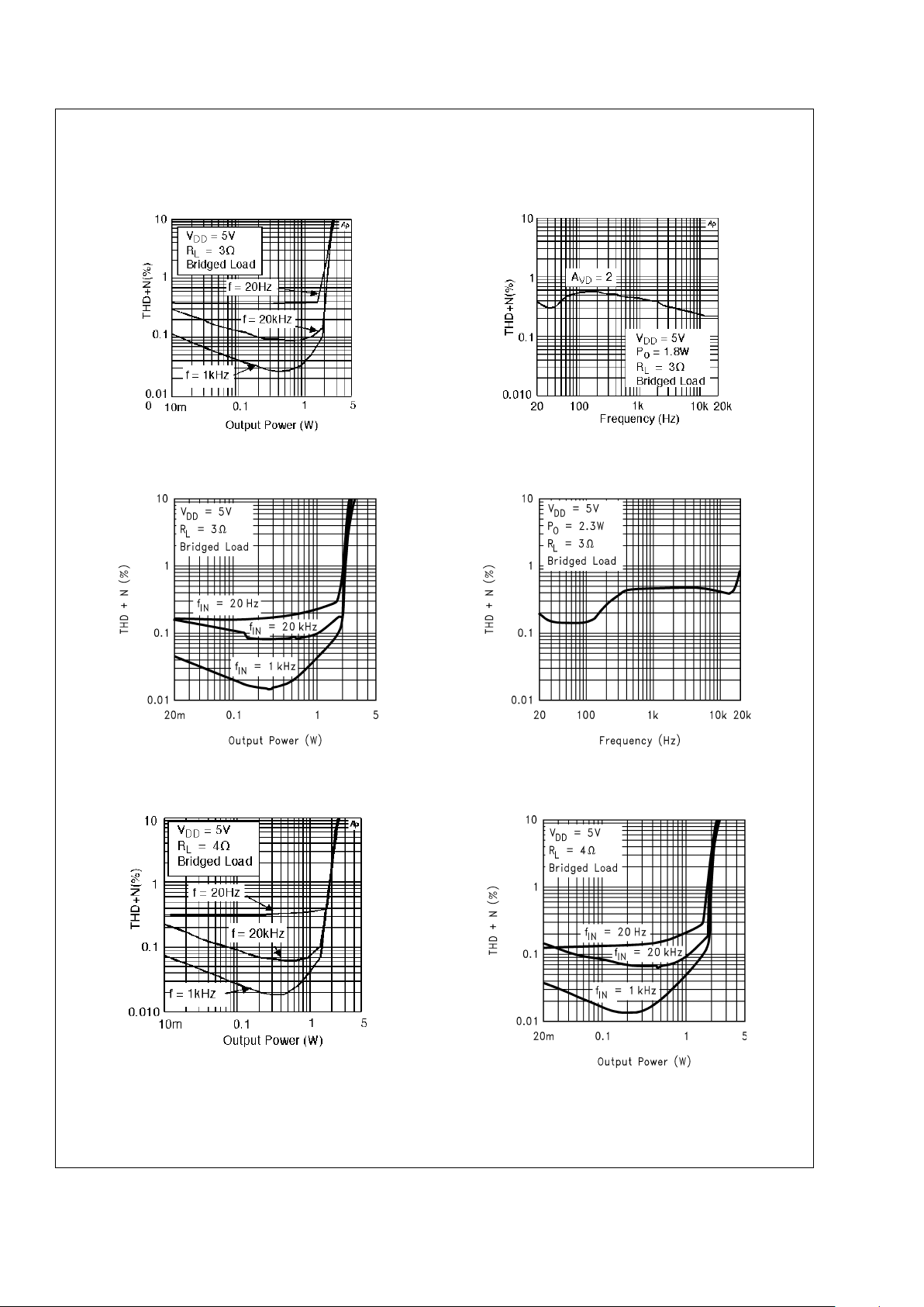
Typical Performance Characteristics
MTE- and LQ- Specific Characteristics
LM4868MTE
THD+N vs Output Power
LM4868MTE
THD+N vs Frequency
20026733
20026734
LM4868LQ
THD+N vs Output Power
LM4868LQ
THD+N vs Frequency
20026753 20026754
LM4868MTE
THD+N vs Output Power
LM4868LQ
THD+N vs Output Power
20026736
20026755
LM4868
www.national.com5
Typical Performance Characteristics
MTE- and LQ- Specific Characteristics
(Continued)
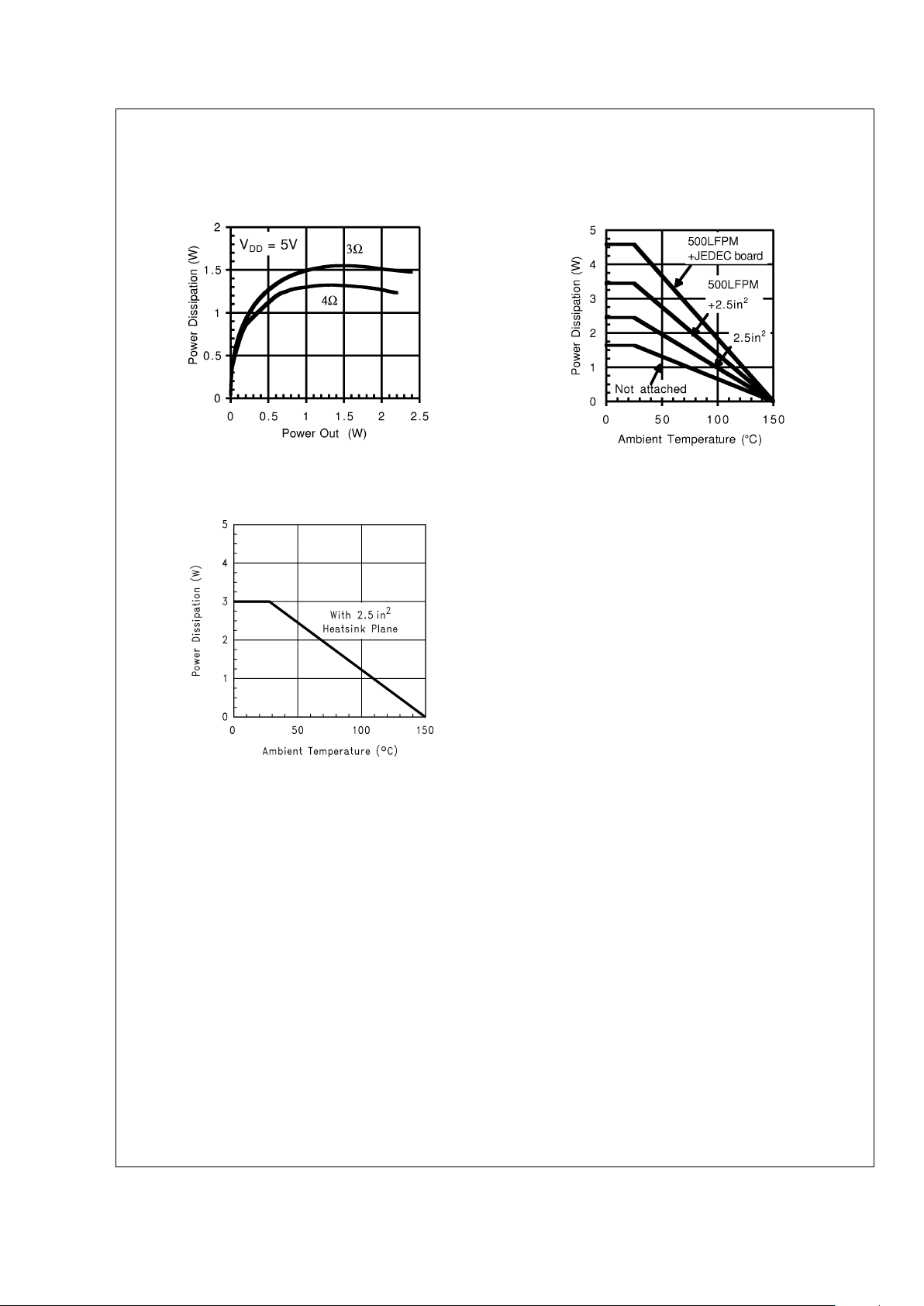
LM4868LQ, LM4868MTE
Power Dissipation vs Power Output
LM4868MTE (Note 18)
Power Derating Curve
20026761
20026759
LM4868LQ
Power Derating Curve
20026769
Note 18: This curve shows the LM4868MTE’s thermal dissipation ability at different ambient temperatures given these conditions:
500LFPM + JEDEC board: The part is soldered to a 1S2P 20-lead exposed-DAP TSSOP test board with 500 linear feet per minute of forced-air flow across
it. Board information - copper dimensions: 74x74mm, copper coverage: 100% (buried layer) and 12% (top/bottom layers), 16 vias under the exposed-DAP.
500LFPM + 2.5in
2
: The part is soldered to a 2.5in2, 1 oz. copper plane with 500 linear feet per minute of forced-air flow across it.
2.5in
2
: The part is soldered to a 2.5in2, 1oz. copper plane.
Not Attached: The part is not soldered down and is not forced-air cooled.
LM4868
www.national.com 6
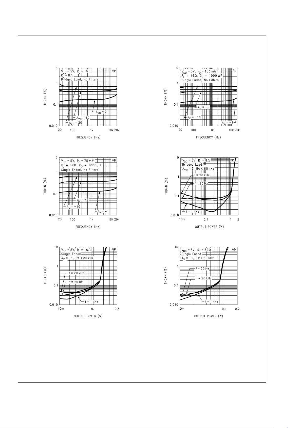
Typical Performance
Characteristics
THD+N vs Frequency THD+N vs Frequency
20026703 20026704
THD+N vs Frequency THD+N vs Output Power
20026705 20026706
THD+N vs Output Power THD+N vs Output Power
20026707 20026708
LM4868
www.national.com7
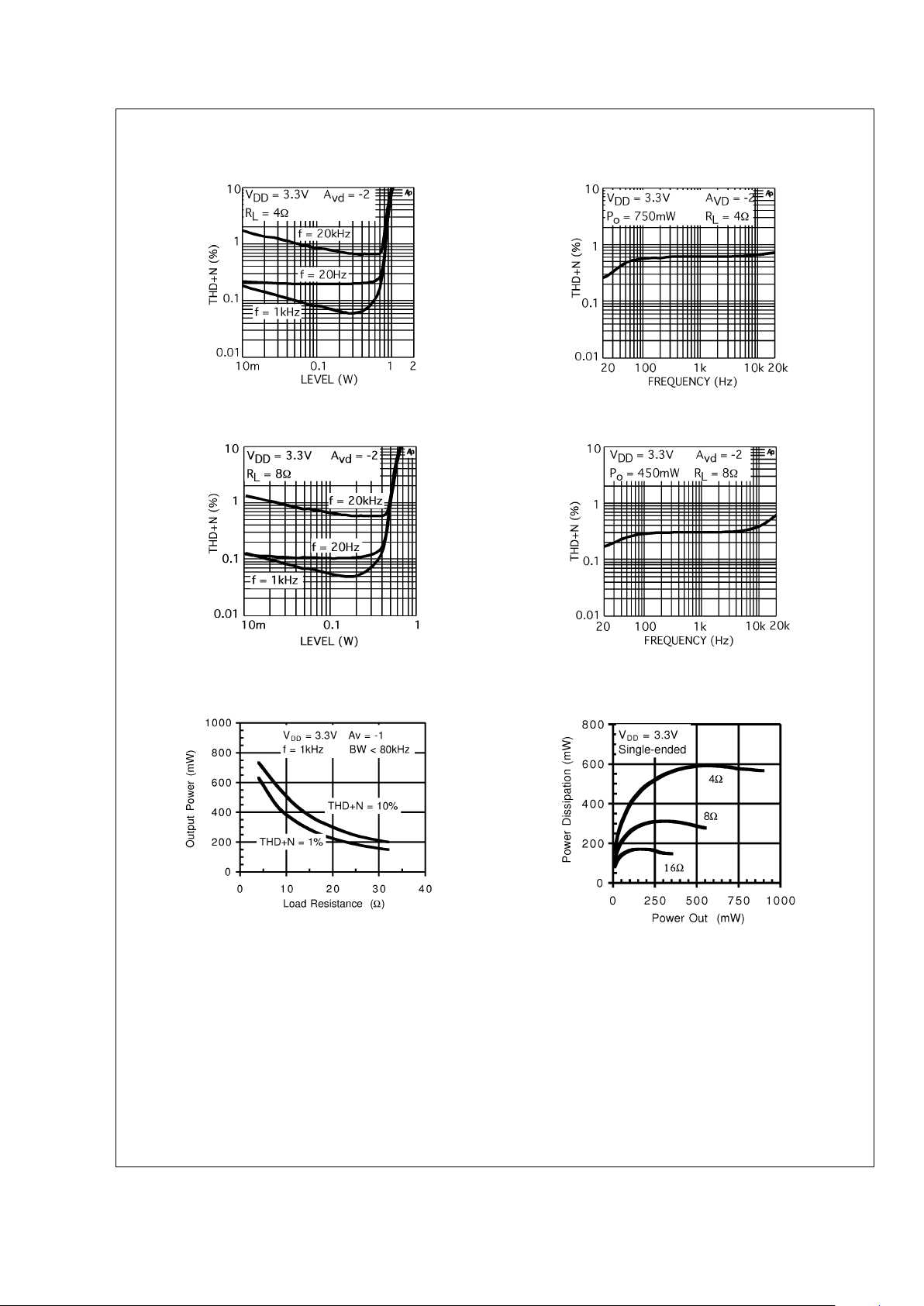
Typical Performance Characteristics (Continued)
THD+N vs Output Power THD+N vs Frequency
20026765
20026763
THD+N vs Output Power THD+N vs Frequency
20026766 20026764
Output Power vs
Load Resistance
Power Dissipation vs
Supply Voltage
20026762
20026760
LM4868
www.national.com 8
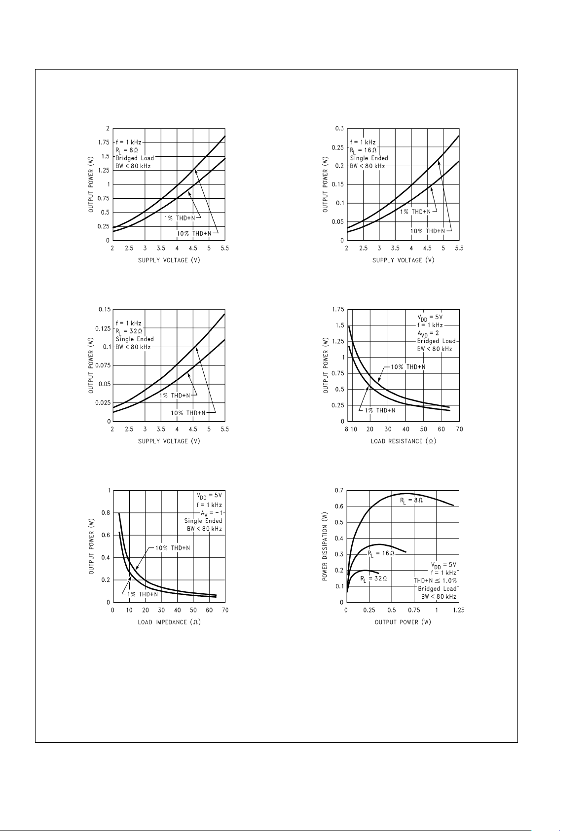
Typical Performance Characteristics (Continued)
Output Power vs
Supply Voltage
Output Power vs
Supply Voltage
20026709 20026710
Output Power vs
Supply Voltage
Output Power vs
Load Resistance
20026711
20026712
Output Power vs
Load Resistance
Power Dissipation vs
Output Power
20026713 20026714
LM4868
www.national.com9
 Loading...