

NSC LM4866MTEX, LM4866MTE, LM4866MT, LM4866LQX, LM4866LQ Datasheet
...
LM4866
2.2W Stereo Audio Amplifier
General Description
The LM4866 is a bridge-connected (BTL) stereo audio
power amplifier which, when connected to a 5V supply,
delivers 2.2W to a 4Ω load (Note 1) or 2.5W to a 3Ω load
(Note 2) with less than 1.0% THD+N.
With the LM4866 packaged in the LLP, the customer benefits
include low thermal impedance, low profile, and small size.
This package minimizes PCB area and maximizes output
power.
The LM4866 features an externally controlled, low-power
consumption shutdown mode, and thermal shutdown protection. It also utilizes circuitry to reduce “clicks and pops”
during device turn-on.
Boomer audio power amplifiers are designed specifically to
use few external components and provide high quality output
power in a surface mount package.
Note 1: An LM4866MTE or LM4866LQ that has been properly mounted to
a circuit board will deliver 2.2W into 4Ω. The other package options for the
LM4866 will deliver 1.1W into 8Ω. See the Application Information sections
for further information concerning the LM4866MTE and LM4866LQ.
Note 2: An LM4866MTE or LM4866LQ that has been properly mounted to a
circuit board will deliver 2.5W into 3Ω.
Key Specifications
n POat 1% THD+N
n LM4866LQ, 3Ω,4Ω loads 2.5W(typ), 2.2W(typ)
n LM4866MTE, 3Ω,4Ω loads 2.5W(typ), 2.2W(typ)
n LM4866MTE, 8Ω load 1.1W(typ)
n LM4866MT, 8Ω load 1.1W(typ)
n Shutdown current 0.7µA(typ)
n Supply voltage range 2.0V to 5.5V
Features
n Stereo BTL amplifier mode
n “Click and pop” suppression circuitry
n Unity-gain stable
n Thermal shutdown protection circuitry
n TSSOP and Exposed-DAP LLP packages
Applications
n Multimedia monitors
n Portable and desktop computers
n Portable televisions
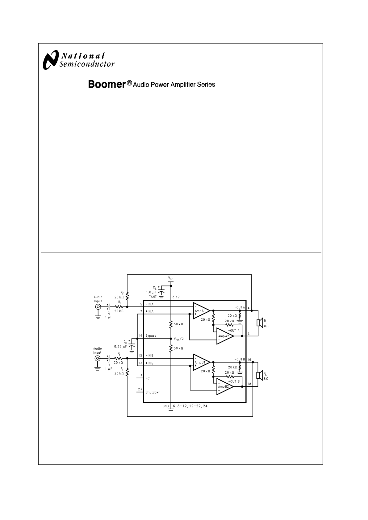
Typical Application
20018601
Note: Pin out shown for LLP package. Refer to the Connection Diagrams for the pinout of the TSSOP package.
Boomer®is a registered trademark of National Semiconductor Corporation.
October 2002
LM4866 2.2W Stereo Audio Amplifier
© 2002 National Semiconductor Corporation DS200186 www.national.com
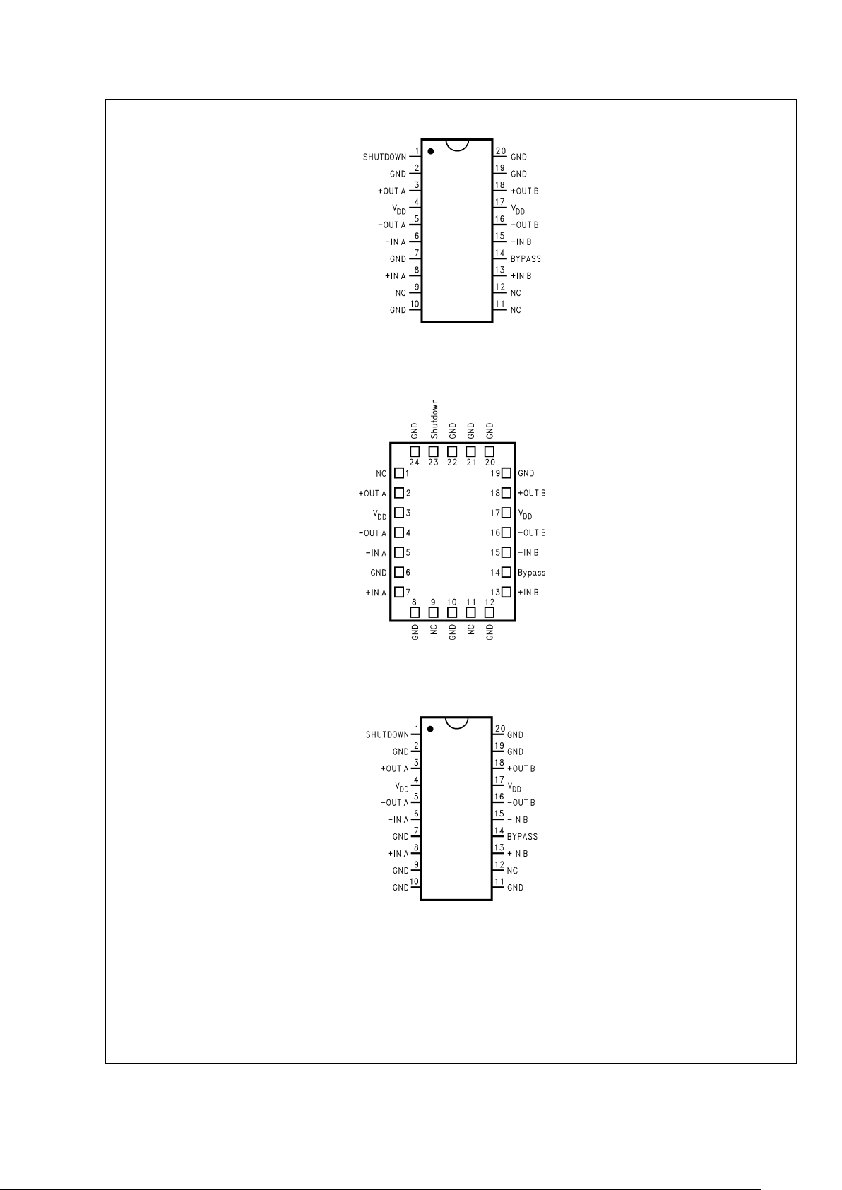
Connection Diagrams
20018629
Top View
Order Number LM4866MT
See NS Package Number MTC20 for TSSOP
20018630
Top View
Order Number LM4866LQ
See NS Package Number LQA24A for Exposed-DAP LLP
20018643
Top View
Order Number LM4866MTE
See NS Package Number MXA20A for Exposed-DAP TSSOP
LM4866
www.national.com 2
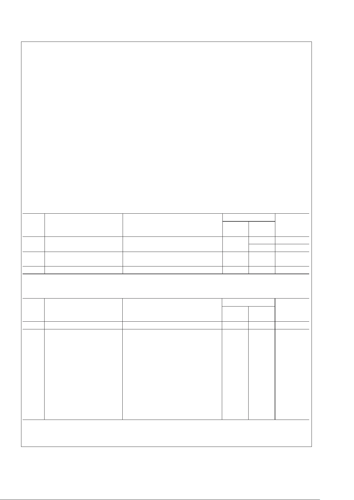
Absolute Maximum Ratings (Note 3)
If Military/Aerospace specified devices are required,
please contact the National Semiconductor Sales Office/
Distributors for availability and specifications.
Supply Voltage 6.0V
Storage Temperature −65˚C to +150˚C
Input Voltage −0.3V to V
DD
+0.3V
Power Dissipation (Note 4) Internally limited
ESD Susceptibility(Note 5) 2000V
ESD Susceptibility (Note 6) 200V
Junction Temperature 150˚C
Solder Information
Small Outline Package
Vapor Phase (60 sec.) 215˚C
Infrared (15 sec.) 220˚C
See AN-450 “Surface Mounting and their Effects on
Product Reliablilty” for other methods of soldering
surface mount devices.
Thermal Resistance
θ
JC
(typ) — MTC20 20˚C/W
θ
JA
(typ) — MTC20 80˚C/W
θ
JC
(typ) — LQ24A 3.0˚C/W
θ
JA
(typ) — LQ24A 42˚C/W (Note 7)
θ
JC
(typ) — MXA20A 2˚C/W
θ
JA
(typ) — MXA20A 41˚C/W (Note 8)
θ
JA
(typ) — MXA20A 51˚C/W (Note 9)
θ
JA
(typ) — MXA20A 90˚C/W (Note 10)
Operating Ratings
Temperature Range
T
MIN
≤ TA≤ T
MAX
−40˚C ≤ TA≤ 85˚C
Supply Voltage 2.0V ≤ V
DD
≤ 5.5V
Electrical Characteristics for Entire IC (Notes 3, 11)
The following specifications apply for VDD= 5V unless otherwise noted. Limits apply for TA= 25˚C.
Symbol Parameter Conditions LM4866 Units
(Limits)
Typical Limit
(Note 12) (Note 13)
V
DD
Supply Voltage 2 V (min)
5.5 V (max)
I
DD
Quiescent Power Supply Current VIN= 0V, IO= 0A (Note 14) 11.5 20
6
mA (max)
mA (min)
I
SD
Shutdown Current VDDapplied to the SHUTDOWN pin 0.7 2 µA (min)
Electrical Characteristics for Bridged-Mode Operation (Notes 3, 11)
The following specifications apply for VDD= 5V unless otherwise specified. Limits apply for TA= 25˚C.
Symbol Parameter Conditions LM4866 Units
(Limits)
Typical Limit
(Note 12) (Note 13)
V
OS
Output Offset Voltage VIN= 0V 5 50 mV (max)
P
O
Output Power (Note 15) THD+N = 1%, f = 1kHz (Note 16)
LM4866MTE, R
L
=3Ω 2.5 W
LM4866LQ, R
L
=3Ω 2.5 W
LM4866MTE, R
L
=4Ω 2.2 W
LM4866LQ, R
L
=4Ω 2.2 W
LM4866MT, R
L
=8Ω 1.1 1.0 W (min)
THD+N = 10%, f = 1kHz
LM4866MTE, R
L
=3Ω 3.2 W
LM4866LQ, R
L
=3Ω 3.2 W
LM4866MTE, R
L
=4Ω 2.7 W
LM4866LQ, R
L
=4Ω 2.7 W
LM4866MT, R
L
=8Ω 1.5 W
LM4866
www.national.com3
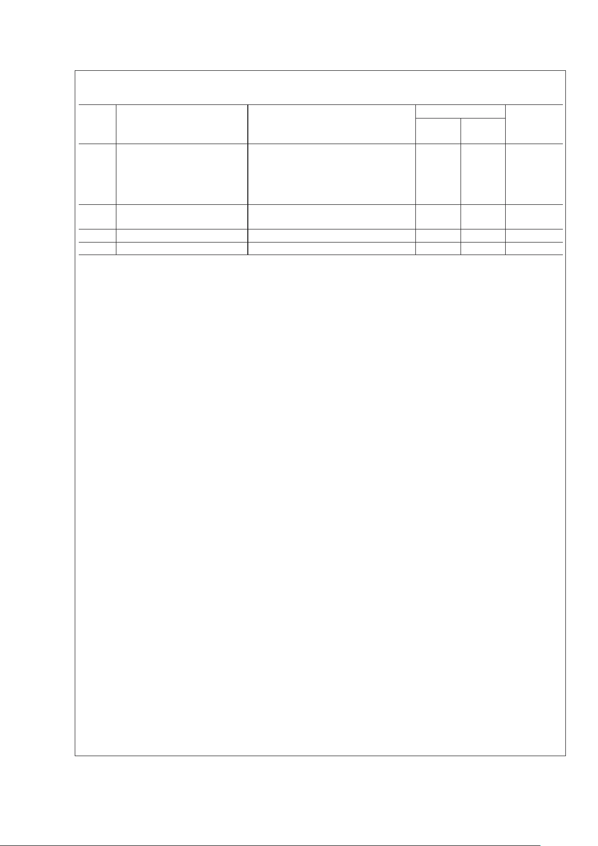
Electrical Characteristics for Bridged-Mode Operation (Notes 3, 11) (Continued)
The following specifications apply for VDD= 5V unless otherwise specified. Limits apply for TA= 25˚C.
Symbol Parameter Conditions LM4866 Units
(Limits)
Typical Limit
(Note 12) (Note 13)
THD+N Total Harmonic Distortion+Noise 20Hz ≤ f ≤ 20kHz, A
VD
=2
LM4866MTE, R
L
=4Ω,PO=2W
LM4866LQ, R
L
=4Ω,PO=2W
LM4866MT, R
L
=4Ω,PO=1W
0.3
0.3
0.3
LM4866MT, R
L
=8Ω,PO= 1W 0.3 %
PSRR Power Supply Rejection Ratio V
DD
= 5V, V
RIPPLE
= 200mV
RMS,RL
=8Ω,
C
B
= 1.0µF
67 dB
X
TALK
Channel Separation f = 1kHz, CB= 1.0µF 90 dB
SNR Signal To Noise Ratio V
DD
= 5V, PO= 1.1W, RL=8Ω 98 dB
Note 3: Absolute Maximum Ratings indicate limits beyond which damage to the device may occur. Operating Ratings indicate conditions for which the device is
functional, but do not guarantee specific performance limits. Electrical Characteristics state DC and AC electrical specifications under particular test conditions which
guarantee specific performance limits. This assumes that the device is within the Operating Ratings. Specifications are not guaranteed for parameters where no limit
is given, however, the typical value is a good indication of device performance.
Note 4: The maximum power dissipation is dictated by T
JMAX
, θJA, and the ambient temperature TAand must be derated at elevated temperatures. The maximum
allowable power dissipation is P
DMAX
=(T
JMAX−TA
)/θJA. For the LM4866, T
JMAX
= 150˚C. For the θJAs for different packages, please see the Application
Information section or the Absolute Maximum Ratings section.
Note 5: Human body model, 100pF discharged through a 1.5kΩ resistor.
Note 6: Machine model, 220pF– 240pF discharged through all pins.
Note 7: The given θ
JA
is for an LM4866 packaged in an LQA24A with the exposed−DAP soldered to an exposed 2in2area of 1oz printed circuit board copper.
Note 8: The given θ
JA
is for an LM4866 packaged in an MXA20A with the exposed−DAP soldered to an exposed 2in2area of 1oz printed circuit board copper.
Note 9: The given θ
JA
is for an LM4866 packaged in an MXA20A with the exposed−DAP soldered to an exposed 1in2area of 1oz printed circuit board copper.
Note 10: The given θ
JA
is for an LM4866 packaged in an MXA20A with the exposed−DAP not soldered to prinbted circuit board copper.
Note 11: All voltages are measured with respect to the ground (GND) pins unless otherwise specified.
Note 12: Typicals are measured at 25˚C and represent the parametric norm.
Note 13: Datasheet min/max specification limits are guaranteed by design, test, or statistical analysis.
Note 14: The quiescent power supply current depends on the offset voltage when a practical load is connected to the amplifier.
Note 15: Output power is measured at the device terminals.
Note 16: When driving 3Ω or 4Ω loads and operating on a 5V supply, the LM4866LQ and LM4866MTE must be mounted to a circuit board that has a minimum of
2.5in
2
of exposed, uninterrupted copper area connected to the package’s exposed DAP.
LM4866
www.national.com 4
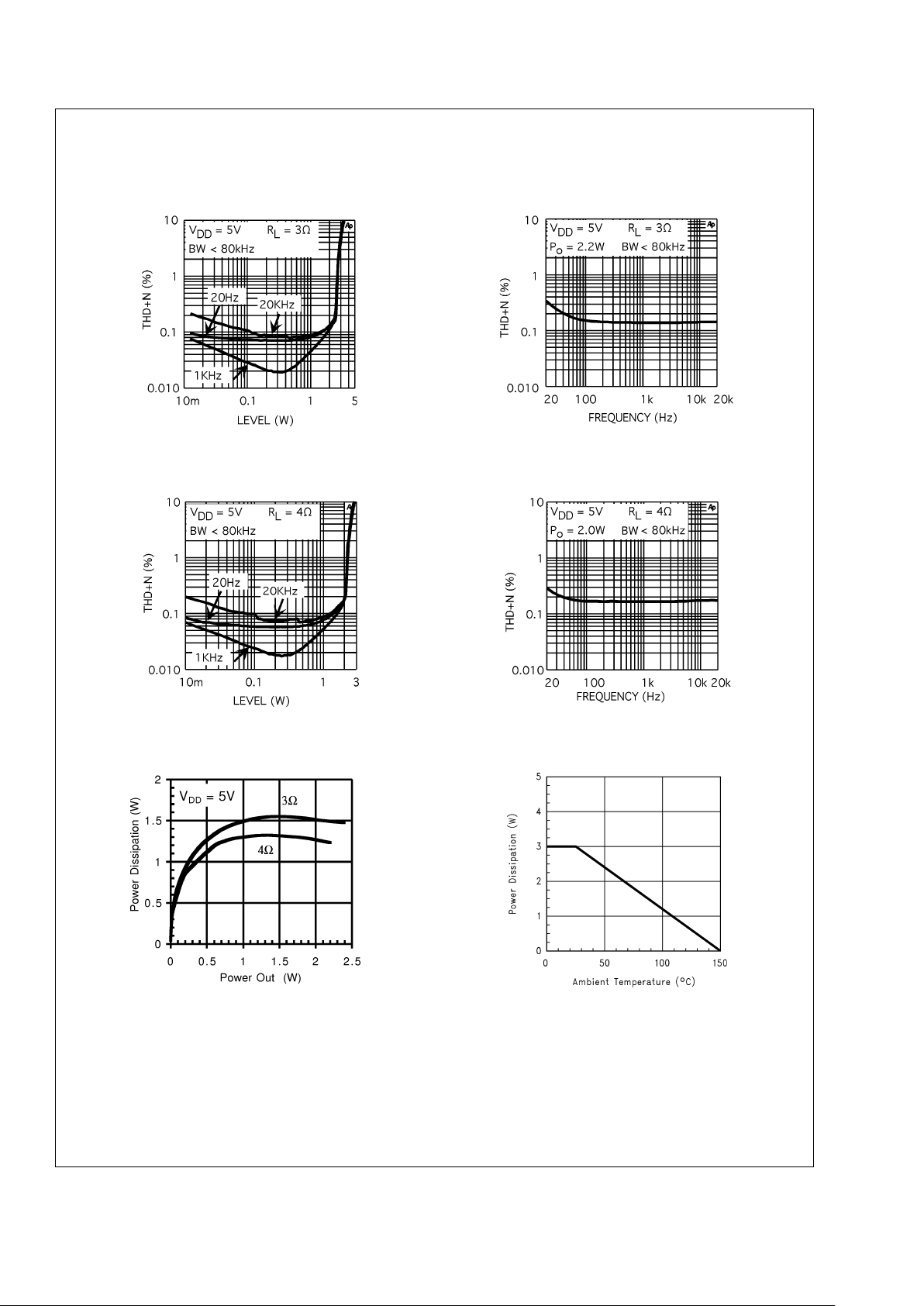
Typical Performance Characteristics
LQ Specific Characteristics
LM4866LQ
THD+N vs Output Power
LM4866LQ
THD+N vs Frequency
20018666
20018668
LM4866LQ
THD+N vs Output Power
LM4866LQ
THD+N vs Frequency
20018665
20018667
LM4866LQ
Power Dissipation vs Power Output
LM4866LQ (Note 17)
Power Derating Curve
20018664
20018695
Note 17: This curve shows the LM4866LQ’s thermal dissipation ability at different ambient temperatures given this condition:
The LLP package’s DAP is soldered to a 2.5in
2
, 1oz. copper plane.
LM4866
www.national.com5
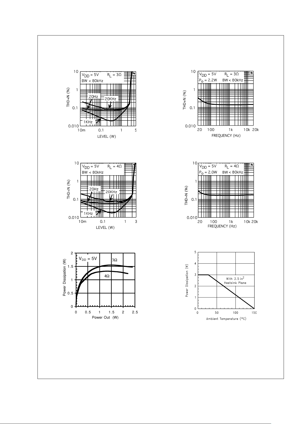
Typical Performance Characteristics
MTE Specific Characteristics
LM4866MTE
THD+N vs Output Power
LM4866MTE
THD+N vs Frequency
20018637
20018638
LM4866MTE
THD+N vs Output Power
LM4866MTE
THD+N vs Frequency
20018639
20018640
LM4866MTE
Power Dissipation vs Power Output
LM4866MTE(Note 18)
Power Derating Curve
20018641
20018642
Note 18: This curve shows the LM4866MTE’s thermal dissipation ability at different ambient temperatures given these conditions:
500LFPM + JEDEC board: The part is soldered to a 1S2P 20-lead exposed-DAP TSSOP test board with 500 linear feet per minute of forced-air flow across
it. Board information - copper dimensions: 74x74mm, copper coverage: 100% (buried layer) and 12% (top/bottom layers), 16 vias under the exposed-DAP.
500LFPM + 2.5in
2
: The part is soldered to a 2.5in2, 1 oz. copper plane with 500 linear feet per minute of forced-air flow across it.
2.5in
2
: The part is soldered to a 2.5in2, 1oz. copper plane.
Not Attached: The part is not soldered down and is not forced-air cooled.
LM4866
www.national.com 6
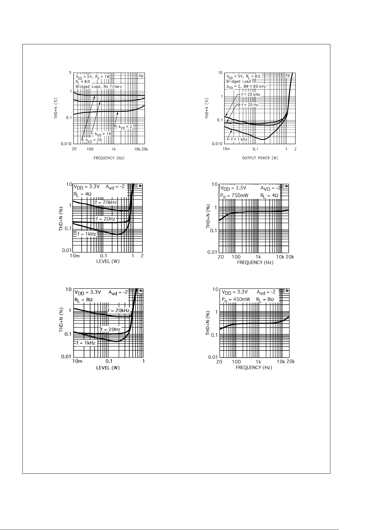
Typical Performance Characteristics
THD+N vs Frequency THD+N vs Output Power
20018603 20018606
THD+N vs Output Power THD+N vs Frequency
20018661
20018663
THD+N vs Output Power THD+N vs Frequency
20018660 20018662
LM4866
www.national.com7
 Loading...