

NSC LM4863N, LM4863MX, LM4863MTX, LM4863MTE, LM4863MT Datasheet
...
LM4863
Dual 2.2W Audio Amplifier Plus Stereo Headphone
Function
General Description
The LM4863 is a dual bridge-connected audio power amplifier which, when connected to a 5V supply, will deliver 2.2W
toa4Ωload (Note 1) or2.5W to a 3Ω load (Note 2)with less
than 1.0%THD+N. In addition, the headphone input pin allows the amplifiers to operate in single-ended mode to drive
stereo headphones.
Boomer audio power amplifiers were designed specifically to
provide high quality output power from a surface mount
package while requiring few external components. To simplify audio system design, the LM4863 combines dual bridge
speaker amplifiers and stereo headphone amplifiers on one
chip.
The LM4863 features an externally controlled, low-power
consumption shutdown mode, a stereo headphone amplifier
mode, and thermal shutdown protection. It also utilizes circuitry to reduce “clicks and pops” during device turn-on.
Note 1: An LM4863MTE which has been properly mounted to the circuit
board will deliver 2.2W into 4Ω. The other package options for the LM4863
will deliver 1.1W into 8Ω. See the Application Information section for
LM4863MTE usage information.
Note 2: An LM4863MTE which has been properly mounted to the circuit
board and forced-air cooled will deliver 2.5W into 3Ω.
Key Specifications
n POat 1%THD+N
into 3Ω (LM4863MTE) 2.5W(typ)
into 4Ω (LM4863MTE) 2.2W(typ)
into 8Ω (LM4863) 1.1W(typ)
n Single-ended mode - THD+N
at 75mW into 32Ω
0.5%(max)
n Shutdown current 0.7µA(typ)
Features
n Stereo headphone amplifier mode
n “Click and pop” suppression circuitry
n Unity-gain stable
n Thermal shutdown protection circuitry
n Exposed-DAP TSSOP, TSSOP, SOIC and DIP
packaging available
Applications
n Multimedia monitors
n Portable and desktop computers
n Portable televisions
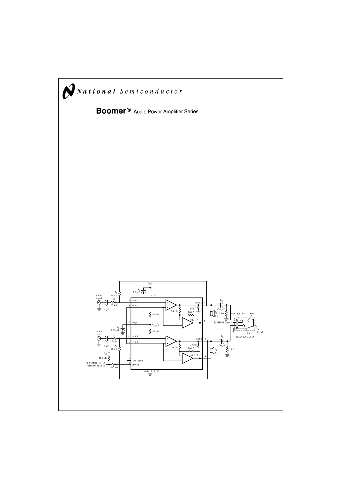
Typical Application
Boomer®is a registered trademark of National Semiconductor Corporation.
DS012881-1
*
Refer to the section Proper Selection of External Components, for a detailed discussion of CBsize.
FIGURE 1. Typical Audio Amplifier Application Circuit
October 1999
LM4863 Dual 2.2W Audio Amplifier Plus Stereo Headphone Function
© 1999 National Semiconductor Corporation DS012881 www.national.com
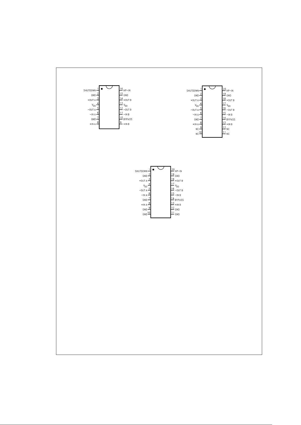
Connection Diagrams
DS012881-28
Top View
Order Number LM4863M, LM4863N
See NS Package Number M16B for SO
See NS Package Number N16A for DIP
DS012881-29
Top View
Order Number LM4863MT
See NS Package Number MTC20 for TSSOP
DS012881-2
Top View
Order Number LM4863MTE
See NS Package Number MXA20A for Exposed-DAP TSSOP
LM4863
www.national.com 2
Absolute Maximum Ratings (Note 4)
If Military/Aerospace specified devices are required,
please contact the National Semiconductor Sales Office/
Distributors for availability and specifications.
Supply Voltage 6.0V
Storage Temperature −65˚C to +150˚C
Input Voltage −0.3V to V
DD
+0.3V
Power Dissipation (Note 10) Internally limited
ESD Susceptibility (Note 11) 2000V
ESD Susceptibility (Note 12) 200V
Junction Temperature 150˚C
Solder Information
Small Outline Package
Vapor Phase (60 sec.) 215˚C
Infrared (15 sec.) 220˚C
See AN-450 “Surface Mounting and their Effects on
Product Reliablilty” for other methods of soldering surface
mount devices.
Thermal Resistance
θ
JC
(typ)—M16B 20˚C/W
θ
JA
(typ)—M16B 80˚C/W
θ
JC
(typ)—N16A 20˚C/W
θ
JA
(typ)—N16A 63˚C/W
θ
JC
(typ)—MTC20 20˚C/W
θ
JA
(typ)—MTC20 80˚C/W
θ
JC
(typ)—MXA20A 2˚C/W
θ
JA
(typ)—MXA20A 41˚C/W (Note 7)
θ
JA
(typ)—MXA20A 51˚C/W (Note 5)
θ
JA
(typ)—MXA20A 90˚C/W (Note 6)
Operating Ratings
Temperature Range
T
MIN
≤ TA≤ T
MAX
−40˚C ≤ TA≤ 85˚C
Supply Voltage 2.0V ≤ V
DD
≤ 5.5V
Electrical Characteristics for Entire IC (Notes 3, 4)
The following specifications apply for V
DD
=
5V unless otherwise noted. Limits apply for T
A
=
25˚C.
Symbol Parameter Conditions LM4863 Units
(Limits)
Typical Limit
(Note 13) (Note 14)
V
DD
Supply Voltage 2 V (min)
5.5 V (max)
I
DD
Quiescent Power Supply Current V
IN
=
0V, I
O
=
0A (Note 15) , HP-IN=0V 11.5 20 mA (max)
6 mA (min)
V
IN
=
0V, I
O
=
0A (Note 15) , HP-IN=4V 5.8 mA
I
SD
Shutdown Current V
PIN1
=
V
DD
0.7 2 µA (min)
V
IH
Headphone High Input Voltage 4 V (min)
V
IL
Headphone Low Input Voltage 0.8 V (max)
Electrical Characteristics for Bridged-Mode Operation (Notes 3, 4)
The following specifications apply for V
DD
=
5V unless otherwise specified. Limits apply for T
A
=
25˚C.
Symbol Parameter Conditions LM4863 Units
(Limits)
Typical Limit
(Note
13)
(Note
14)
V
OS
Output Offset Voltage V
IN
=
0V 5 50 mV (max)
P
O
Output Power (Note 9) THD=1%,f=1 kHz
LM4863MTE, R
L
=
3Ω (Note 7)
2.5 W
LM4863MTE, R
L
=
4Ω (Note 8) 2.2 W
LM4863, R
L
=
8Ω 1.1 1.0 W (min)
THD+N=10%,f=1 kHz
LM4863MTE, R
L
=
3Ω (Note 7) 3.2 W
LM4863MTE, R
L
=
4Ω (Note 8) 2.7
LM4863, R
L
=
8Ω 1.5 W
THD+N=1%,f=1 kHz, R
L
=
32Ω 0.34 W
THD+N Total Harmonic Distortion+Noise 20 Hz ≤ f ≤ 20 kHz, A
VD
=
2
LM4863MTE, R
L
=
4Ω,P
O
=
2W
0.3
LM4863, R
L
=
8Ω,P
O
=
1W 0.3
%
PSRR Power Supply Rejection Ratio V
DD
=
5V, V
RIPPLE
=
200 mV
RMS,RL
=
8Ω,
C
B
=
1.0 µF
67 dB
LM4863
www.national.com3
Electrical Characteristics for Bridged-Mode Operation (Notes 3, 4) (Continued)
The following specifications apply for V
DD
=
5V unless otherwise specified. Limits apply for T
A
=
25˚C.
Symbol Parameter Conditions LM4863 Units
(Limits)
Typical Limit
(Note
13)
(Note
14)
X
TALK
Channel Separation f=1 kHz, C
B
=
1.0 µF 90 dB
SNR Signal To Noise Ratio V
DD
=
5V, P
O
= 1.1W, RL=8Ω 98 dB
Electrical Characteristics for Single-Ended Operation (Notes 3, 4)
The following specifications apply for V
DD
=
5V unless otherwise specified. Limits apply for T
A
=
25˚C.
Symbol Parameter Conditions LM4863 Units
(Limits)
Typical Limit
(Note
13)
(Note
14)
V
OS
Output Offset Voltage V
IN
=
0V 5 50 mV (max)
P
O
Output Power THD=0.5%,f=1 kHz, R
L
=
32Ω 85 75 mW (min)
THD+N=1%,f=1 kHz, R
L
=
8Ω 340 mW
THD+N=10%,f=1 kHz, R
L
=
8Ω 440 mW
THD+N Total Harmonic Distortion+Noise A
V
=
−1, P
O
=
75 mW, 20 Hz ≤ f ≤ 20 kHz,
R
L
=
32Ω
0.2
%
PSRR Power Supply Rejection Ratio C
B
=
1.0 µF, V
RIPPLE
=
200 mV
RMS
,
f=1 kHz
52 dB
X
TALK
Channel Separation f=1 kHz, C
B
=
1.0 µF 60 dB
SNR Signal To Noise Ratio V
DD
=
5V, P
O
= 340mW, RL=8Ω 95 dB
Note 3: All voltages are measured with respect to the ground pins, 2, 7, and 15, unless otherwise specified.
Note 4: Absolute Maximum Ratings indicate limits beyond which damage to the devicemayoccur.OperatingRatings indicate conditions for which the device is func-
tional, but donotguaranteespecificperformancelimits.Electrical Characteristics state DC and AC electricalspecificationsunderparticulartestconditionswhich guarantee specific performance limits. This assumes that the device is within the Operating Ratings. Specifications are not guaranteed for parameters where no limit is
given, however, the typical value is a good indication of device performance.
Note 5: The θ
JA
given is for an MXA20A package whose exposed-DAP is soldered to an exposed 2in2piece of 1 ounce printed circuit board copper.
Note 6: The θ
JA
given is for an MXA20A package whose exposed-DAP is not soldered to any copper.
Note 7: When driving 3Ω loads from a 5V supply, the LM4863MTE must be mounted to the circuit board and forced-air cooled (450 linear-feet per minute).
Note 8: When driving 4Ω loads from a 5V supply, the LM4863MTE must be mounted to the circuit board.
Note 9: Output power is measured at the device terminals.
Note 10: The maximum power dissipation must be derated at elevated temperatures and is dictated by T
JMAX
, θJA, and the ambient temperature TA. The maximum
allowable power dissipation is P
DMAX
=
(T
JMAX−TA
)/θJA. For the LM4863, T
JMAX
=
150˚C. For the θ
JA
s for different packages, please see the Application Informa-
tion section or the Absolute Maximum Ratings section.
Note 11: Human body model, 100 pF discharged through a 1.5 kΩ resistor.
Note 12: Machine model, 220 pF–240 pF discharged through all pins.
Note 13: Typicals are measured at 25˚C and represent the parametric norm.
Note 14: Limits are guaranteed to National’s AOQL (Average Outgoing Quality Level).
Note 15: The quiescent power supply current depends on the offset voltage when a practical load is connected to the amplifier.
Truth Table for Logic Inputs
SHUTDOWN HP-IN LM4863 MODE
Low Low Bridged
Low High Single-Ended
High Low LM4863 Shutdown
High High LM4863 Shutdown
LM4863
www.national.com 4
External Components Description
(
Figure 1
)
Components Functional Description
1. R
i
Inverting input resistance which sets the closed-loop gain in conjunction with Rf. This resistor also forms a
high pass filter with C
i
at f
c
=
1/(2πR
iCi
).
2. C
i
Input coupling capacitor which blocks the DC voltage at the amplifier’s input terminals. Also creates a
highpass filter with R
i
at f
c
=
1/(2πR
iCi
). Refer to the section, Proper Selection of External Components,
for an explanation of how to determine the value of C
i
.
3. R
f
Feedback resistance which sets the closed-loop gain in conjunction with Ri.
4. C
s
Supply bypass capacitor which provides power supply filtering. Refer to the Power Supply Bypassing
section for information concerning proper placement and selection of the supply bypass capacitor.
5. C
B
Bypass pin capacitor which provides half-supply filtering. Refer to the section, Proper Selection of
External Components, for information concerning proper placement and selection of C
B
.
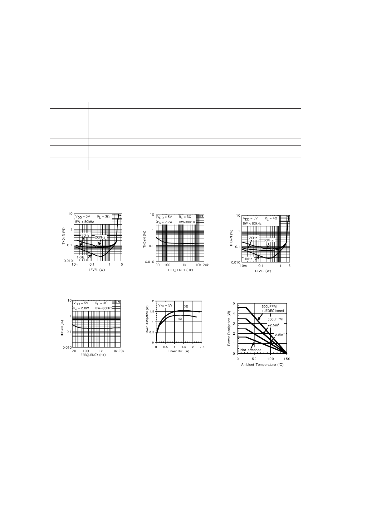
Typical Performance Characteristics
MTE Specific Characteristics
Note 16: These curves show the thermal dissipation ability of the LM4863MTE at different ambient temperatures given these conditions:
500LFPM + JEDEC board: The part is soldered to a 1S2P 20-lead exposed-DAP TSSOP test board with 500 linear feet per minute of forced-air flow across
it. Board information - copper dimensions: 74x74mm, copper coverage: 100%(buried layer) and 12%(top/bottom layers), 16 vias under the exposed-DAP.
500LFPM + 2.5in
2
: The part is soldered to a 2.5in2, 1 oz. copper plane with 500 linear feet per minute of forced-air flow across it.
2.5in
2
: The part is soldered to a 2.5in2, 1oz. copper plane.
Not Attached: The part is not soldered down and is not forced-air cooled.
LM4863MTE
THD+N vs Output Power
DS012881-97
LM4863MTE
THD+N vs Frequency
DS012881-99
LM4863MTE
THD+N vs Output Power
DS012881-96
LM4863MTE
THD+N vs Frequency
DS012881-98
LM4863MTE
Power Dissipation vs Power Output
DS012881-90
LM4863MTE(Note 16)
Power Derating Curve
DS012881-95
LM4863
www.national.com5
 Loading...