

NSC LM4854MTX, LM4854MT, LM4854LD, LM4854IBLX, LM4854IBL Datasheet
...
LM4854
1.9W Monaural, 85mW Stereo Headphone Audio
Amplifier
General Description
The unity-gain stable LM4854 is both a mono differential
output (for bridge-tied loads, or BTL) audio power amplifier
and a single-ended (SE) stereo headphone amplifier. Operating on a single 5V supply, the mono BTL mode delivers
1.1W (typ) to an 8Ω load, 1.7W (typ) to a 4Ω load (Note 1) at
1% THD+N. In SE stereo mode, the amplifier will deliver
85mW to 32Ω loads. The LM4854 features a new circuit
topology that suppresses output transients (’click and pops’)
and eliminates SE-mode output coupling capacitors, saving
both component and board space costs. The LM4854 has
three inputs: one pair for a two-channel stereo signal and the
third for a single-channel mono input.
The LM4854 is designed for PDA, cellular telephone, notebook, and other handheld portable applications. It delivers
high quality output power from a surface-mount package and
requires few external components. Other features include an
active-low micropower shutdown mode, an "instant-on" low
power standby mode, and thermal shutdown protection.
The LM4854 is available in the very space-efficient 12-lead
micro SMD, exposed-DAP LLP for higher power applications, and TSSOP packages.
Note 1: An LM4854LD that has been properly mounted to a circuit board will
deliver 1.7W (typ) into a 4Ω load.
Key Specifications
j
LLP BTL output power (RL= 3.2Ω and
THD+N = 1%)
VDD= 3.0V 1.0W (typ)
V
DD
= 5.0V 1.9W (typ)
j
LLP BTL output power (RL=4Ω and
THD+N = 1%)
VDD= 3.0V 900mW (typ)
V
DD
= 5.0V 1.7W (typ)
j
LLP BTL output power (RL=8Ω and
THD+N = 1%)
VDD= 3.0V 380mW (typ)
V
DD
= 5.0V 1.1W (typ)
j
SE output power (RL=32Ω and THD+N
= 1.0%)
V
DD
= 3.0V 32mW (typ)
V
DD
= 5.0V 93mW (typ)
j
Micropower shutdown supply current
V
DD
= 3.0V 0.005µA (typ)
V
DD
= 5.0V 0.05µA (typ)
j
Standby supply current
V
DD
= 3.0V 16µA (typ)
V
DD
= 5.0V 27µA (typ)
j
PSRR (f = 1kHz, 3.0V ≤ VDD≤ 5.0V,
(Fig. 1))
BTL 60dB (typ)
SE 66dB (typ)
Features
n Fast 0.1ms (typ) and 1.0ms (max) turn-on and turn-off
time
n Eliminates SE amplifier output coupling capacitors
n Advanced "click and pop" suppression circuitry
n Stereo headphone amplifier mode
n Low-power standby and ultra-low current micropower
shutdown modes
n Thermal shutdown protection circuitry
n 2.4V to 5.5V operation
n Unity-gain stable
n Gain set with external resistors
n Space-saving micro SMD package, exposed-DAP LLP,
and TSSOP
Applications
n PDAs
n Notebook computers
n Cellular phones
n Handheld portable electronic devices
Boomer®is a registered trademark of National Semiconductor Corporation.
April 2003
LM4854 1.9W Monaural, 85mW Stereo Headphone Audio Amplifier
© 2003 National Semiconductor Corporation DS200382 www.national.com
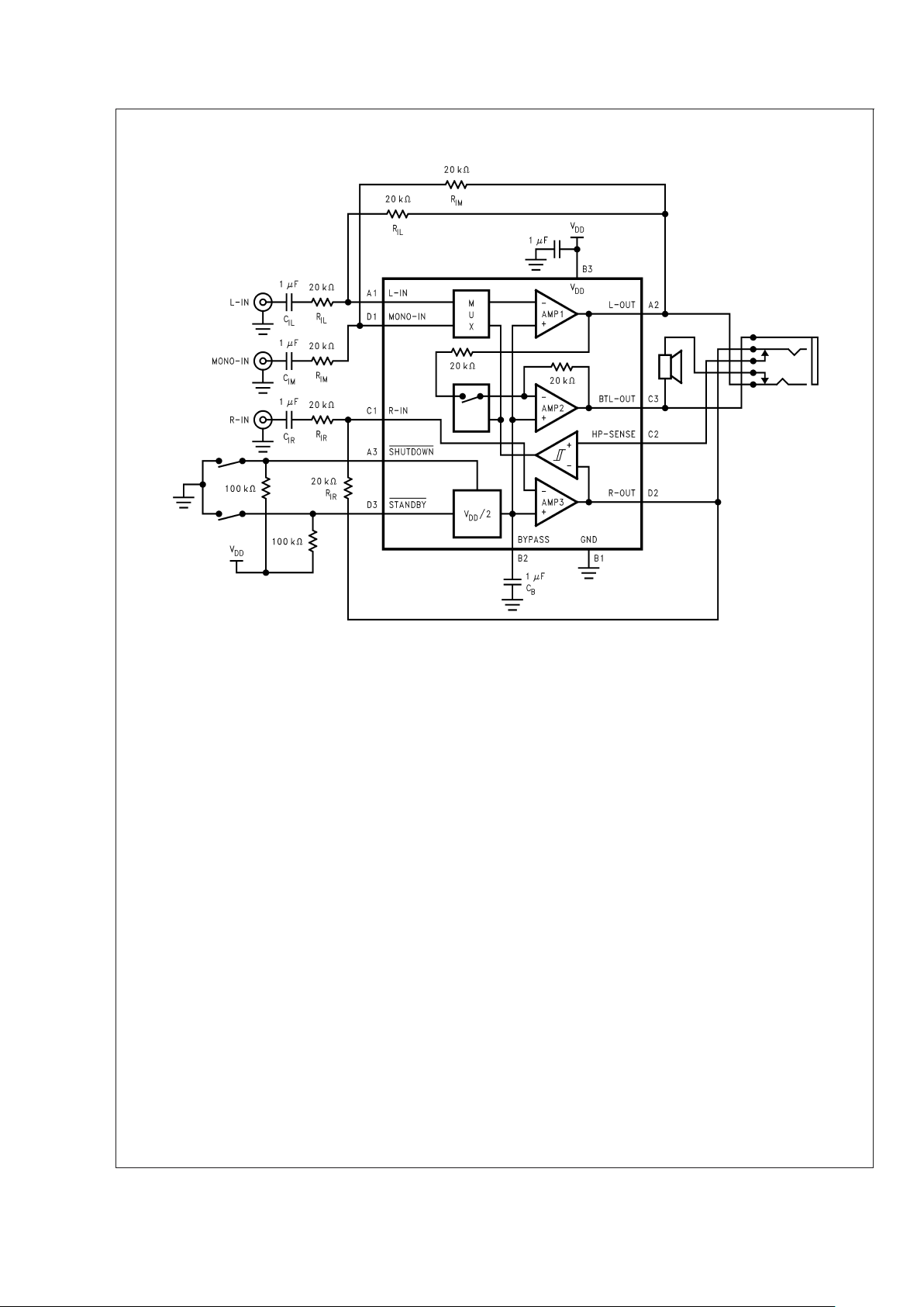
Typical Application
(Pin out shown for the 12-pin large bump micro SMD IBL package. Consult the "Connection Diagrams" for the LLP or MT
package pin out.)
20038201
FIGURE 1. Typical Audio Amplifier Application Circuit
LM4854
www.national.com 2
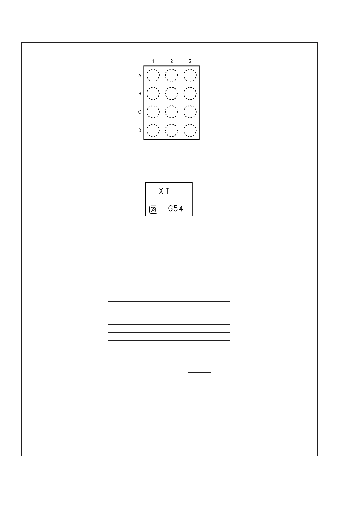
Connection Diagrams
20038202
Top View (Bump-side down)
Order Number LM4854IBL
See NS Package Number BLA12BAB
Micro SMD Marking
20038203
Top View
X - Date Code
T - Die Traceability
G - Boomer Family
54 - LM4854IBL
LM4854IBL Pin Designation
Pin (Bump) Number Pin Function
A1 L-IN
B1 GND
C1 R-IN
D1 MONO-IN
A2 L-OUT
B2 BYPASS
C2 HP-SENSE
D2 R-OUT
A3 SHUTDOWN
B3 V
DD
C3 BTL-OUT
D3 STANDBY
LM4854
www.national.com3
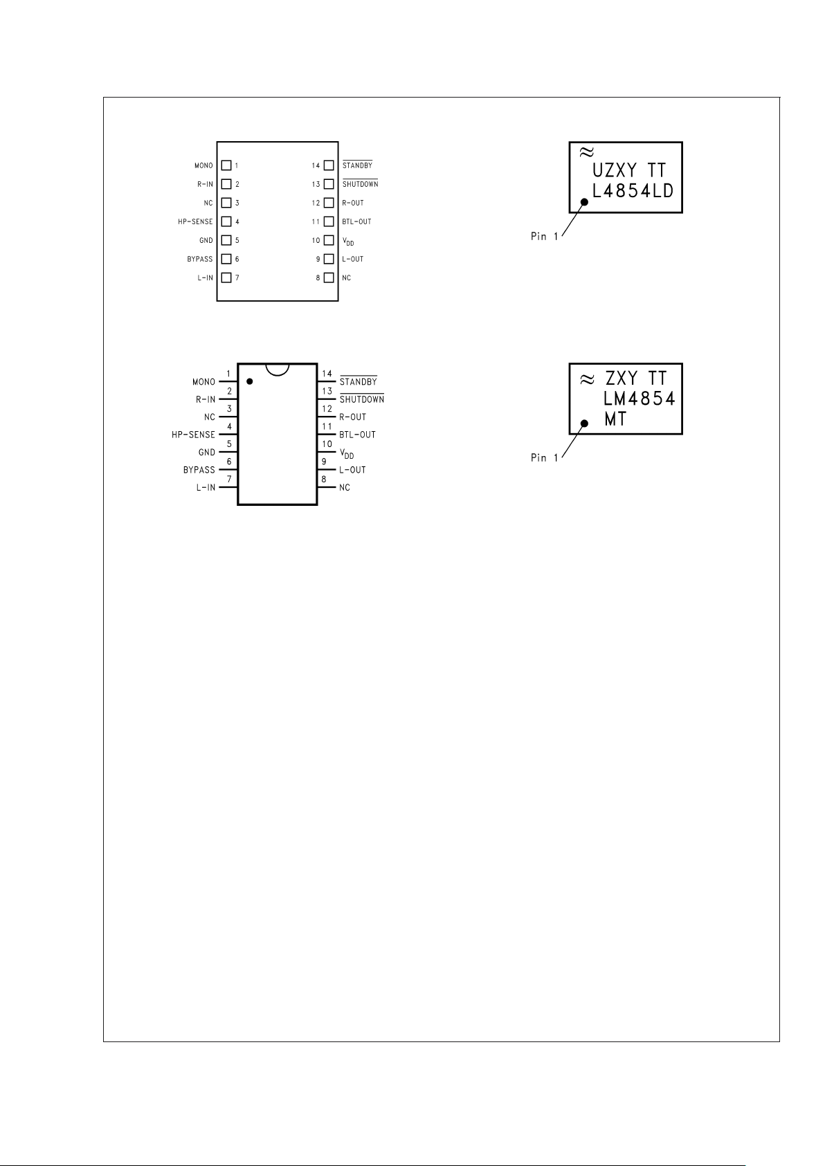
Connection Diagrams
20038204
Top View
Order Number LM4854LD
See NS Package Number LDA14A
200382A5
Top View
U - Fab Code
Z - Plant Code
XY - Date Code
TT - Die Tracebility
Bottom Line - Part Number
20038205
Top View
Order Number LM4854MT
See NS Package Number MTC14
200382A6
Top View
Z - Plant Code
XY - Date Code
TT - Die Traceability
Bottom 2 lines - Part Number
LM4854
www.national.com 4
Absolute Maximum Ratings (Notes 2,
3)
If Military/Aerospace specified devices are required,
please contact the National Semiconductor Sales Office/
Distributors for availability and specifications.
Supply Voltage 6.0V
Storage Temperature −65˚C to +150˚C
Input Voltage −0.3V to V
DD
+ 0.3V
Power Dissipation(Note 4) Internally Limited
ESD Susceptibility (Note 5)
All pins except Pin C3 (IBL), Pin11
(LD/MT) 2000V
Pin C3 (IBL), Pin 11 (LD/MT) 8000V
ESD Susceptibility(Note 6) 200V
Junction Temperature (T
J
) 150˚C
Solder Information
Small Outline Package
Vapor Phase (60 sec.) 215˚C
Infrared (15 sec.) 220˚C
See AN-540 "Surface Mounting and
their Effects on Product Reliability"
for other methods of soldering
surface-mount devices.
Thermal Resistance
θ
JA
(typ) — BLA12BAB 121˚C/W
θ
JC
(typ) — LDA14A 3˚C/W
θ
JA
(typ) — LDA14A 42˚C/W (Note 7)
θ
JC
(typ) — MTC14 40˚C/W
θ
JA
(typ) — MTC14 109˚C/W
Operating Ratings (Note 3)
Temperature Range
T
MIN
≤ TA≤ T
MAX
−40˚C ≤ TA≤ +85˚C
Supply Voltage 2.4V ≤ V
DD
≤ 5.5V
Electrical Characteristics for Entire Amplifier (VDD= 5V)
The following specifications apply for circuit shown in Figure 1, unless otherwise specified. Limits apply for TA= 25˚C.
Symbol Parameter Conditions LM4854 Units
(Limits)
Typical
(Note 8)
Limit
(Notes 9,
10)
I
DD
Quiescent Power Supply Current VIN= 0V; IO= 0A, No Load 5.0 12 mA max)
V
IN
= 0V; IO= 0A, 8Ω Load 6.5 15 mA (max)
I
STBY
Standby Quiescent Power Supply
Current
V
STANDBY
= GND 27 35 µA (max)
I
SD
Shutdown Quiescent Power
Supply Current
V
SHUTDOWN
= GND 0.05 0.2 µA (max)
V
OS
Output Offset Voltage 8Ω Load 2.0 40 mV (max)
PSRR Power Supply Rejection Ratio C
BYPASS
= 1.0µF, R
SOURCE
=10Ω
V
RIPPLE
= 200mV
p-p
sinewave
BTL, R
L
=8Ω,RIN=10Ω
f
IN
= 217Hz
f
IN
= 1kHz
SE, R
L
=32Ω,RIN=10Ω
f
IN
= 217Hz
f
IN
= 1kHz
61
63
dB
dB
68
71
dB
dB
t
RSH
Return-from-Shutdown Time C
BYPASS
= 1.0µF 200 ms
t
RST
Return-from-Standby Time 0.1 1.0 ms(max)
V
IH
Shutdown or Standby Logic High
Treshold
1.4 V (min)
V
IL
Shutdown or Standby Logic Low
Treshold
0.4 V (max)
LM4854
www.national.com5
Electrical Characteristics Bridged-Mode Operation (VDD= 5V)
The following specifications apply for for the circuit shown in Figure 1 and a measurement bandwith of 20Hz to 80kHz, unless
otherwise specified. Limits apply for T
A
= 25˚C.
Symbol Parameter Conditions LM4854 Units
(Limits)
Typical
(Note 8)
Limit
(Notes 9,
10)
P
O
Output Power (Note 11) THD = 1% (max); f = 1kHz (Note12)
R
L
= 3.2Ω (LM4854LD)
R
L
=4Ω (LM4854LD)
R
L
=8Ω
1.9
1.7
1.1 1.0
W
W
W (min)
THD = 10% (max); f = 1kHz (Note12)
R
L
= 3.2Ω (LM4854LD)
R
L
=4Ω (LM4854LD)
R
L
=8Ω
2.3
2.1
1.3
W
W
W
THD+N Total Harmonic Distortion+Noise 20Hz ≤ f
IN
≤ 20kHz
R
L
=4Ω,PO= 1.0W (LM4854LD)
R
L
=8Ω,PO= 400mW
0.3
0.18
%
%
f
IN
= 1kHz
R
L
=4Ω,PO= 1.5W (LM4854LD)
R
L
=8Ω,PO= 50mW
0.1
0.08
%
%
S/N Signal-to-Noise Ratio f
IN
= 1kHz, C
BYPASS
= 1.0µF
P
O
= 900mW, RL=8Ω 90 dB
Electrical Characteristics : SE Operation (VDD= 5V)
The following specifications apply for for the circuit shown in Figure 1 and a measurement bandwith of 20Hz to 80kHz, unless
otherwise specified. Limits apply for T
A
= 25˚C.
Symbol Parameter Conditions LM4854 Units
(Limits)
Typical
(Note 8)
Limit
(Notes 9,
10)
P
O
Output Power (Note 11) THD+N = 1.0%, f = 1kHz, RL=32Ω
THD+N = 10%, f = 1kHz, R
L
=32Ω
THD+N = 1.0%, f = 1kHz, R
L
=16Ω
THD+N = 10%, f = 1kHz, R
L
=16Ω
93
105
170
200
85
140
mW(min)
mW
mW(min)
mW
THD+N Total Harmonic Distortion+Noise 20Hz ≤ f
IN
≤ 20kHz
R
L
=32Ω,PO= 50mW 0.3 %
VOUT Output Voltage Swing THD = 1.0%, R
L
=5kΩ 4.0 V
P-P
XTALK Channel Separation fIN= 1kHz, C
BYPASS
= 1.0µF, RL=32Ω 55 dB
S/N Signal-to-Noise Ratio f
IN
= 1kHz, C
BYPASS
= 1.0µF
P
O
= 50mW, RL=32Ω 90 dB
Electrical Characteristics for Entire Amplifier (VDD= 3.0V)
The following specifications apply for circuit shown in Figure 1, unless otherwise specified. Limits apply for TA= 25˚C.
Symbol Parameter Conditions LM4854 Units
(Limits)
Typical
(Note 8)
Limit
(Notes 9,
10)
I
DD
Quiescent Power Supply Current VIN= 0V, IO= 0A, 8Ω Load 4.0 10 mA (max)
I
STBY
Standby Quiescent Power Supply
Current
V
STANDBY
= GND 16.0 20.0 µA (max)
I
SD
Shutdown Current V
SHUTDOWN
= GND 0.005 0.02 µA (max)
V
OS
Output Offset Voltage 8 Ω Load 2.0 40 mV (max)
LM4854
www.national.com 6
Electrical Characteristics for Entire Amplifier (VDD= 3.0V) (Continued)
The following specifications apply for circuit shown in Figure 1, unless otherwise specified. Limits apply for TA= 25˚C.
Symbol Parameter Conditions LM4854 Units
(Limits)
Typical
(Note 8)
Limit
(Notes 9,
10)
PSRR Power Supply Rejection Ratio C
BYPASS
= 1.0µF, R
SOURCE
=10Ω
V
RIPPLE
= 200mV
p-p
sinewave
BTL, R
L
=8Ω,RIN=10Ω
f
IN
= 217Hz
f
IN
= 1kHz
SE, R
L
=32Ω,RIN=10Ω
f
IN
= 217Hz
f
IN
= 1kHz
62
62
dB
dB
68
72
dB
dB
t
RSH
Return-from-Shutdown Time C
BYPASS
= 1.0µF 200 ms
t
RST
Return-from-Standby Time 0.1 1.0 ms(max)
V
IH
Shutdown or Standby Logic High
Treshold
1.4 V (min)
V
IL
Shutdown or Standby Logic Low
Treshold
0.4 V (max)
Electrical Characteristics : Bridged-Mode Operation (VDD= 3.0V) (Notes 4, 9)
The following specifications apply for for the circuit shown in Figure 1 and a measurement bandwith of 20Hz to 80kHz, unless
otherwise specified. Limits apply for T
A
= 25˚C.
Symbol Parameter Conditions LM4854 Units
(Limits)
Typical
(Note 8)
Limit
(Notes 9,
10)
P
O
Output Power (Note11) THD = 1% (max); f = 1kHz (Note11)
R
L
=4Ω (LM4854LD)
R
L
=8Ω
1.0
380 350
W
mW (min)
THD = 10% (max); f = 1kHz (Note11)
RL=4Ω (LM4854LD)
R
L
=8Ω
1.1
530
W
mW
THD+N Total Harmonic Distortion+Noise 20Hz ≤ f
IN
≤ 20kHz
R
L
=4Ω,PO= 800mW (LM4854LD)
R
L
=8Ω,PO= 150mW
0.3
0.21
%
%
f
IN
= 1kHz
R
L
=4Ω,PO= 500mW (LM4854LD)
R
L
=8Ω,PO= 150mW
0.1
0.075
%
%
S/N Signal-to-Noise Ratio f
IN
= 1kHz, C
BYPASS
= 1.0µF
P
O
= 900mW, RL=8Ω 90 dB
LM4854
www.national.com7
Electrical Characteristics : SE Operation (VDD= 3.0V) (Notes 4, 9)
The following specifications apply for for the circuit shown in Figure 1 and a measurement bandwith of 20Hz to 80kHz, unless
otherwise specified. Limits apply for T
A
= 25˚C.
Symbol Parameter Conditions LM4854 Units
(Limits)
Typical
(Note 8)
Limit
(Notes 9,
10)
P
O
Output Power (Note 11) THD+N = 1.0%, f = 1kHz, RL=32Ω
THD+N = 10%, f = 1kHz, R
L
=32Ω
THD+N = 1.0%, f = 1kHz, R
L
=16Ω
THD+N = 10%, f = 1kHz, R
L
=16Ω
32
60
57
100
27
38
mW(min)
mW
mW (min)
mW
THD+N Total Harmonic Distortion+Noise 20Hz ≤ f
IN
= ≤ 20kHz
R
L
=32Ω,PO= 30mW 0.3 %
VOUT Output Voltage Swing THD = 0.5%, R
L
=5kΩ 2.4 V
P-P
XTALK Channel Separation fIN= 1kHz, C
BYPASS
= 1.0µF, RL=32Ω 55 dB
S/N Signal-to-Noise Ratio f
IN
= 1kHz, C
BYPASS
= 1.0µF
P
O
= 30mW, RL=32Ω
TBD dB
Note 2: All voltages are measured with respect to the GND pin unless other wise specified.
Note 3: Absolute Maximum Ratings indicate limits beyond which damage to the device may occur. Operating Ratings indicate conditions for which the device is
functional but do not guarantee specific performance limits. Electrical Characteristics state DC and AC electrical specifications under particular test conditions that
guarantee specific performance limits. This assumes that the device is within the Operating Ratings. Specifications are not guaranteed for parameters where no limit
is given, however, the typical value is a good indication of device performance.
Note 4: The maximum power dissipation must be derated at elevated temperatures and is dictated by T
JMAX
, θJA, and the ambient temperature, TA. The maximum
allowable power dissipation is P
DMAX
=(T
JMAX-TA
)/θJAor the number given in Absolute Maximum Ratings, whichever is lower. For the LM4854, see power derating
currents for more information.
Note 5: Human body model, 100pF discharged through a 1.5kΩ resistor.
Note 6: Machine Model, 220pF-240pF discharged through all pins.
Note 7: The given θ
JA
is for an LM4854 packaged in an LDA14A with the Exposed-DAP soldered to an exposed 2in2 area of 1oz printed circuit board copper.
Note 8: Typicals are measured at 25˚C and represent the parametric norm.
Note 9: Limits are guaranteed to National’s AOQL (Average Outgoing Quality Level).
Note 10: Datasheet minimum and maximum specification limits are guaranteed by design, test, or statistical analysis.
Note 11: Output power is measured at the amplifier’s package pins.
Note 12: When driving 4Ω loads and operating on a 5V supply, the LM4854LD must be mounted to a circuit board that has a minimum of 2.5in2 of exposed,
uninterrupted copper area connected to the LLP package’s exposed DAP.
LM4854
www.national.com 8
External Components Description
See Figure 1.
Components Functional Description
1. R
i
This is the inverting input resistance that, along with Rf, sets the closed-loop gain. Input resistance Riand
input capacitance C
i
form a high pass filter. The filter’s cutoff frequency is fc= 1/2πRiCi.
2. C
i
This is the input coupling capacitor. It blocks DC voltage at the amplifier’s inverting input. Ciand Ricreate a
highpass filter. The filter’s cutoff frequency is f
c
= 1/2πRiCi. Refer to the Application Information section,
SELECTING EXTERNAL COMPONENTS, for an explanation of determining C
i
’s value.
3. R
f
This is the feedback resistance that, along with Ri, sets the closed-loop gain.
4. C
s
The supply bypass capacitor. Refer to the POWER SUPPLY BYPASSING section for information about
properly placing, and selecting the value of, this capacitor.
5. C
B
This capacitor filters the half-supply voltage present on the BYPASS pin. Refer to the Application
Information section, SELECTING EXTERNAL COMPONENTS, for information about properly placing, and
selecting the value of, this capacitor..
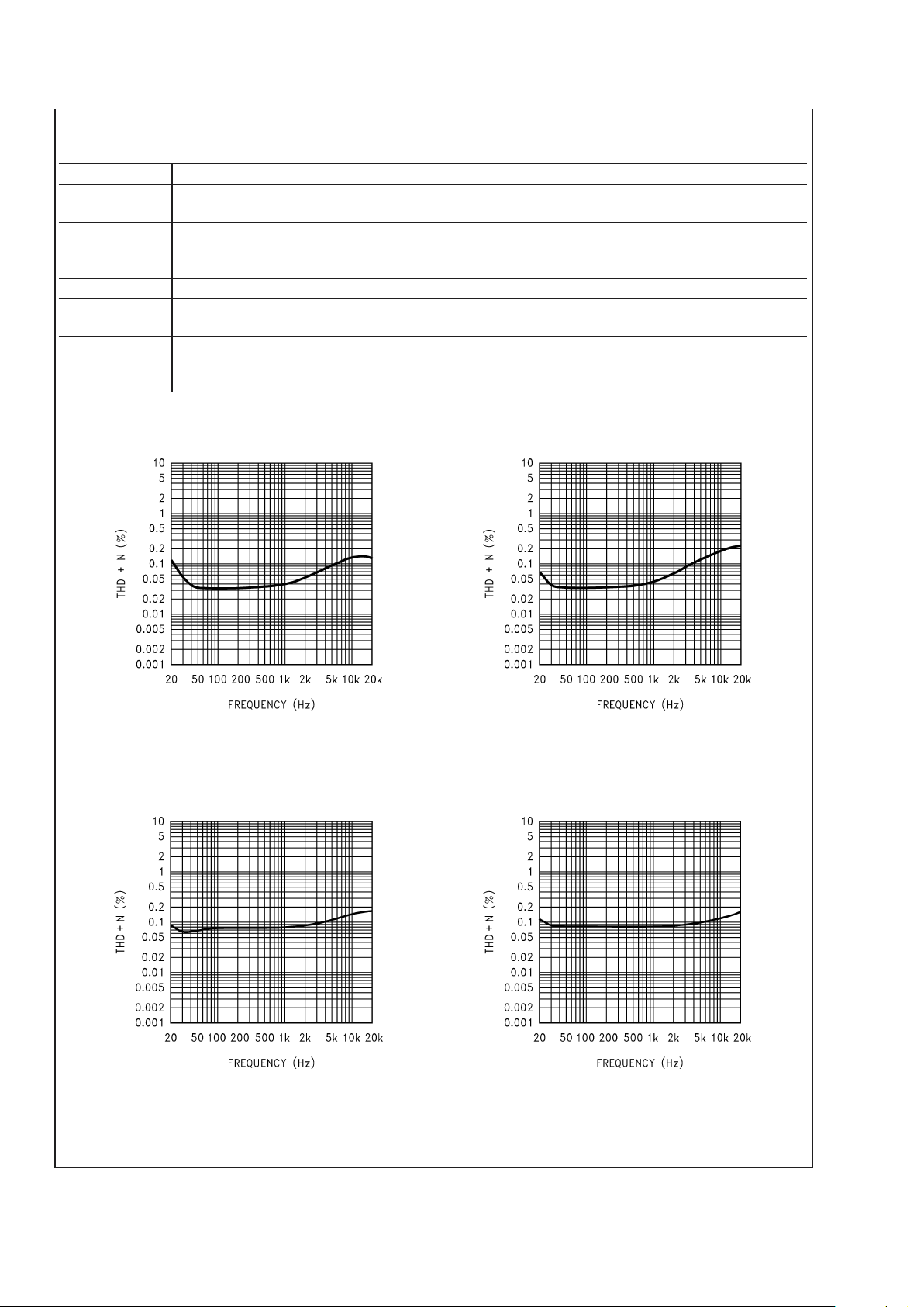
Typical Performance Characteristics
THD+N vs Frequency THD+N vs Frequency
200382D8
LM4854LD
V
DD
= 5V, RL=4Ω (BTL),
P
OUT
= 1000mW
200382D9
LM4854LD
V
DD
= 5V, RL=4Ω (BTL),
P
OUT
= 400mW
THD+N vs Frequency THD+N vs Frequency
200382C0
VDD= 5V, RL=8Ω (BTL),
P
OUT
= 400mW
200382B8
VDD= 5V, RL=16Ω (SE),
P
OUT
= 50mW
LM4854
www.national.com9
 Loading...