

NSC LM4851LQ, LM4851ITLX Datasheet
LM4851
Integrated Audio Amplifier System
General Description
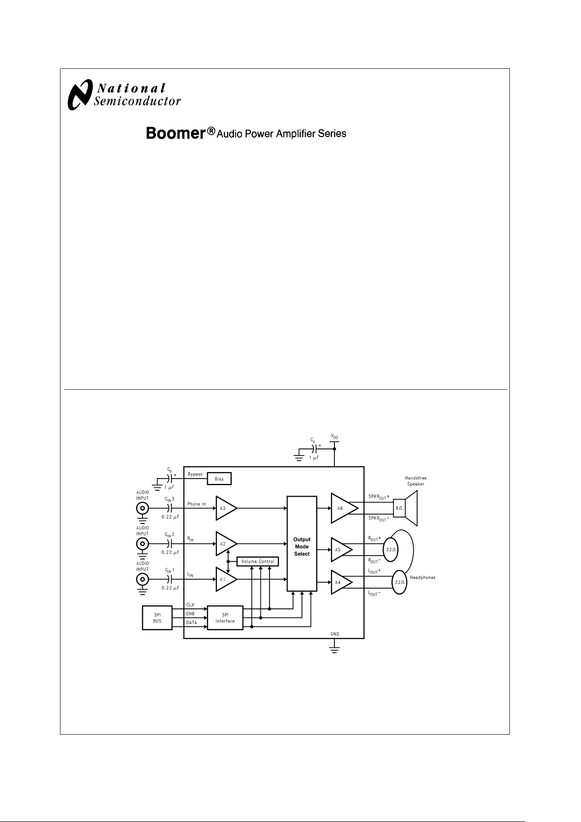
The LM4851 is an audio power amplifier system capable of
delivering 1.1W (typ) of continuous average power into a
mono 8Ω bridged-tied load (BTL) with 1% THD+N and
115mW (typ) per channel of continuous average power into
stereo 32Ω BTL loads with 0.5% THD+N, using a 5V power
supply.
The LM4851 features a 32 step digital volume control and
eight distinct output modes. The digital volume control and
output modes are programmed through a three-wire SPI
serial control interface, that allows flexibility in routing and
mixing audio channels. The LM4851 has 3 inputs: one pair
for a two-channel stereo signal and the third for a singlechannel mono input.
The LM4851 is designed for cellular phone, PDA, and other
portable handheld applications. It delivers high quality output
power from a surface-mount package and requires only five
external components.
The industry leading micro SMD package utilizes only 2mm
x 2.3mm of PCB space, making the LM4851 the most space
efficient audio sub system available today.
Key Specifications
n THD+N at 1kHz, 1.5W into 4Ω BTL (LQ) 1% (typ)
n THD+N at 1kHz, 1.1W into 8Ω BTL 1% (typ)
n THD+N at 1kHz, 115mW into 32Ω BTL 0.5% (typ)
n Single Supply Operation 2.6 to 5.0V
Features
n Mono 1.1W (typ) and stereo 115mW (typ) output
n SPI programmable 32 step digital volume control
(-40.5dB to +6dB)
n Eight distinct SPI programmable output modes
n micro-SMD and LLP surface mount packaging
n “Click and pop” suppression circuitry
n Thermal shutdown protection
n Low shutdown current (0.1µA, typ)
Applications
n Mobile phones
n PDAs
Typical Application
Boomer®is a registered trademark of National Semiconductor Corporation.
20040831
FIGURE 1. Typical Audio Amplifier Application Circuit
December 2002
LM4851 Integrated Audio Amplifier System
© 2002 National Semiconductor Corporation DS200408 www.national.com
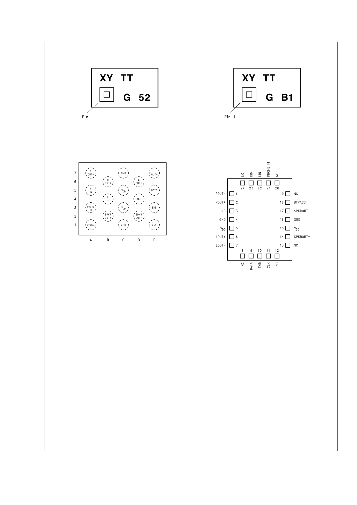
Connection Diagrams
18-Bump micro SMD Marking (IBL) 18-Bump micro SMD Marking (ITL)
200408A5
Top View
XY- Date Code
TT - Die Traceability
G - Boomer Family
52 - LM4851IBL-1
200408B3
Top View
XY- Date Code
TT - Die Traceability
G - Boomer Family
B1 - LM4851ITL
20040829
NC = NO CONNECT
Top View
(Bump-side down)
Order Number LM4851ITL, LM4851IBL
See NS Package Number TLA18AAA, BLA18AAB
200408A7
Top View
Order Number LM4851LQ
See NS Package Number LQA24A for Exposed-DAP LLP
LM4851
www.national.com 2
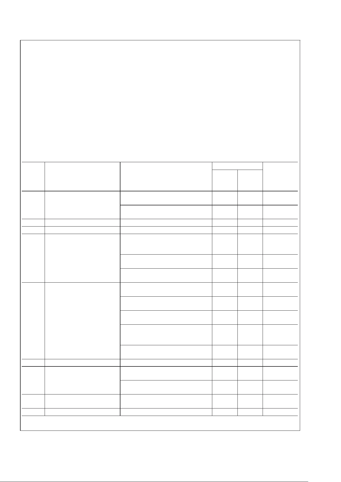
Absolute Maximum Ratings (Note 2)
If Military/Aerospace specified devices are required,
please contact the National Semiconductor Sales Office/
Distributors for availability and specifications.
Supply Voltage 6.0V
Storage Temperature −65˚C to +150˚C
ESD Susceptibility (Note 4) 2.0kV
ESD Machine model (Note 7) 200V
Junction Temperature (T
J
) 150˚C
Solder Information (Note 1)
Vapor Phase (60 sec.) 215˚C
Infrared (15 sec.) 220˚C
Thermal Resistance
θ
JA
(typ) - LQA24A 42˚C/W
θ
JC
(typ) - LQA24A 3.0˚C/W
θ
JA
(typ) - BLA18AAB 48˚C/W (Note 9)
θ
JC
(typ) - BLA18AAB 23˚C/W (Note 9)
θ
JA
(typ) - TLA18AAA 48˚C/W (Note 9)
θ
JC
(typ) - TLA18AAA 23˚C/W (Note 9)
Operating Ratings (Note 3)
Temperature Range −40˚C to 85˚C
Supply Voltage V
DD
2.6V ≤ VDD≤ 5.0V
Note 1: See AN-450 "Surface Mounting and their effects on Product Reliability" for other methods of soldering surface mount devices.
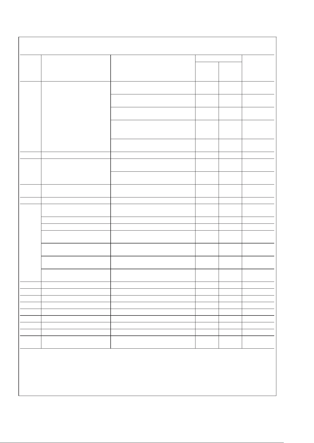
Electrical Characteristics (Notes 2, 8)
The following specifications apply for VDD= 5.0V, TA= 25˚C unless otherwise specified.
Symbol Parameter Conditions LM4851 Units
(Limits)
Typical
(Note 5)
Limit
(Note 6)
I
DD
Supply Current
Output mode 7
V
IN
= 0V; IO=0A
7.5 14 mA (max)
Output modes 1, 2, 3, 4, 5, 6
V
IN
= 0V; IO=0A
5.0 9.0 mA (max)
I
DD
Shutdown Current Output mode 0 0.1 2 µA (max)
V
OS
Output Offset Voltage VIN= 0V 5.0 50 mV (max)
P
O
Output Power
SPKR
OUT;RL
=4Ω
THD+N = 1%; f = 1kHz
LM4851LQ
1.5 W
SPKR
OUT;RL
=8Ω
THD+N = 1%; f = 1kHz
1.1 0.8 W (min)
R
OUT
and L
OUT;RL
=32Ω
THD+N = 0.5%; f = 1kHz
115 80 mW (min)
THD+N
Total Harmonic Distortion Plus
Noise
R
OUT
and L
OUT
; f = 1kHz
P
OUT
= 80mW; RL=32Ω
0.5 % (max)
SPKR
OUT
; f = 1kHz
P
OUT
= 800mW; RL=8Ω
1.0 % (max)
R
OUT
and L
OUT
; f = 20Hz to 20kHz
P
OUT
= 100mW; RL=32Ω
0.3 %
SPKR
OUT
; f = 20Hz to 20kHz
P
OUT
= 1W; RL=4Ω
LM4851LQ
0.3 %
SPKR
OUT
; f = 20Hz to 20kHz
P
OUT
= 800mW; RL=8Ω
0.3 %
N
OUT
Output Noise A-weighted (Note 10) 29 µV
PSRR Power Supply Rejection Ratio V
RIPPLE
= 200mVPP; f = 217Hz
Input floating; Input referred
70 dB
V
RIPPLE
= 200mVPP; f = 217Hz
Input terminated into 50Ω; Output referred
62 dB
V
IH
Logic High Input Voltage 1.4
5.0
V (min)
V (max)
V
IL
Logic Low Input Voltage 0.4 V (max)
LM4851
www.national.com3
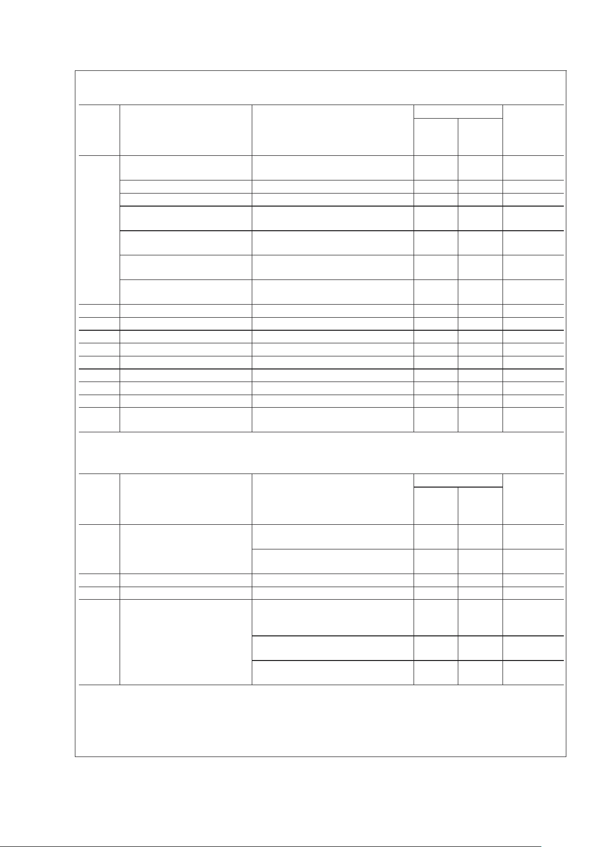
Electrical Characteristics (Notes 2, 8) (Continued)
The following specifications apply for VDD= 5.0V, TA= 25˚C unless otherwise specified.
Symbol Parameter Conditions LM4851 Units
(Limits)
Typical
(Note 5)
Limit
(Note 6)
Digital Volume Range (R
IN
and
L
IN
)
Input referred minimum gain
Input referred maximum gain
-40.5
+6
dB
Digital Volume Stepsize 1.5 dB
Stepsize Error
±
0.5 dB
Phone In Volume BTL gain from
Phone In to SPKR
OUT
6dB
Phone In Volume BTL gain from
Phone In to R
OUT,LOUT
0dB
Phone In Input Impedance 20 15
25
kΩ (min)
kΩ (max)
R
IN
and L
IN
50 37.5
62.5
kΩ (min)
kΩ (max)
t
ES
Enable Setup Time (ENB) 20 ns (min)
t
EH
Enable Hold Time (ENB) 20 ns (min)
t
EL
Enable Low Time (ENB) 30 ns (min)
t
DS
Data Setup Time (DATA) 20 ns (min)
t
DH
Data Hold Time (DATA) 20 ns (min)
t
CS
Clock Setup Time (CLK) 20 ns (min)
t
CH
Clock Logic High Time (CLK) 50 ns (min)
t
CL
Clock Logic Low Time (CLK) 50 ns (min)
t
CLK
Clock Frequency DC
10
(min)
MHz (max)
Electrical Characteristics (Notes 2, 8)
The following specifications apply for VDD= 3.0V, TA= 25˚C unless otherwise specified.
Symbol Parameter Conditions LM4851 Units
(Limits)
Typical
(Note 5)
Limit
(Note 6)
I
DD
Supply Current
Output mode 7
V
IN
= 0V; IO=0A
6.2 11 mA (max)
Output modes 1, 2, 3, 4, 5, 6
VIN= 0V; IO=0A
4.0 7.0 mA (max)
I
DD
Shutdown Current Output mode 0 0.1 2 µA (max)
V
OS
Output Offset Voltage VIN= 0V 5.0 50 mV (max)
P
O
Output Power SPKR
OUT;RL
=4Ω
THD+N = 1%; f = 1kHz
LM4851LQ
430 mW
SPKR
OUT;RL
=8Ω
THD+N = 1%; f = 1kHz
340 300 mW (min)
R
OUT
and L
OUT;RL
=32Ω
THD+N = 0.5%; f = 1kHz
25 20 mW (min)
LM4851
www.national.com 4
Electrical Characteristics (Notes 2, 8) (Continued)
The following specifications apply for VDD= 3.0V, TA= 25˚C unless otherwise specified.
Symbol Parameter Conditions LM4851 Units
(Limits)
Typical
(Note 5)
Limit
(Note 6)
THD+N
Total Harmonic Distortion Plus
Noise
R
OUT
and L
OUT
; f = 1kHz
P
OUT
= 20mW; RL=32Ω
0.5 % (max)
SPKR
OUT
; f = 1kHz
P
OUT
= 300mW; RL=8Ω
1.0 % (max)
R
OUT
and L
OUT
; f = 20Hz to 20kHz
P
OUT
= 20mW; RL=32Ω
0.4 %
SPKR
OUT
; f = 20Hz to 20kHz
P
OUT
= 300mW; RL=4Ω
LM4851LQ
0.3 %
SPKR
OUT
; f = 20Hz to 20kHz
P
OUT
= 250mW; RL=8Ω
0.3 %
N
OUT
Output Noise A-weighted (Note 10) 29 µV
PSRR Power Supply Rejection Ratio V
RIPPLE
= 200mVPP; f = 217Hz
Input floating; Input referred
70 dB
V
RIPPLE
= 200mVPP; f = 217Hz
Input terminated into 50Ω; Output referred
62 dB
V
IH
Logic High Input Voltage 1.4
3.0
V (min)
V (max)
V
IL
Logic Low Input Voltage 0.4 V (max)
Digital Volume Range (R
IN
and
L
IN
)
Input referred minimum gain
Input referred maximum gain
-40.5
+6
dB
Digital Volume Stepsize 1.5 dB
Stepsize Error
±
0.5 dB
Phone In Volume BTL gain from
Phone In to SPKR
OUT
6dB
Phone In Volume BTL gain from
Phone In to R
OUT,LOUT
0dB
Phone In Input Impedance 20 15
25
kΩ (min)
kΩ (max)
R
IN
and L
IN
50 37.5
62.5
kΩ (min)
kΩ (max)
t
ES
Enable Setup Time (ENB) 20 ns (min)
t
EH
Enable Hold Time (ENB) 20 ns (min)
t
EL
Enable Low Time (ENB) 30 ns (min)
t
DS
Data Setup Time (DATA) 20 ns (min)
t
DH
Data Hold Time (DATA) 20 ns (min)
t
CS
Clock Setup Time (CLK) 20 ns (min)
t
CH
Clock Logic High Time (CLK) 50 ns (min)
t
CL
Clock Logic Low Time (CLK) 50 ns (min)
t
CLK
Clock Frequency DC
10
(min)
MHz (max)
Note 2: Absolute Maximum Rating indicate limits beyond which damage to the device may occur.
Note 3: Operating Ratings indicate conditions for which the device is functional, but do not guarantee specific performance limits. For guaranteed specifications and
test conditions, see the Electrical Characteristics. The guaranteed specifications apply only for the test conditions listed. Some performance characteristics may
degrade when the device is not operated under the listed test conditions.
Note 4: Human body model, 100pF discharged through a 1.5kΩ resistor.
Note 5: Typical specifications are specified at +25˚C and represent the most likely parametric norm.
Note 6: Datasheet min/max specification limits are guaranteed by design, test, or statistical analysis.
LM4851
www.national.com5
Note 7: Machine Model ESD test is covered by specification EIAJ IC-121-1981. A 200pF cap is charged to the specified voltage, then discharged directly into the
IC with no external series resistor (resistance of discharge path must be under 50Ω).
Note 8: All voltages are measured with respect to the ground pin, unless otherwise specified.
Note 9: The given θ
JA
and θJCis for an LM4851 mounted on a demonstration board witha4in2area of 1oz printed circuit board copper ground plane.
Note 10: Please refer to the Output Noise vs Output Mode table in the Typical Performance Characteristics section for more details.
External Components Description
Figure 1
Components Functional Description
1. C
in
This is the input coupling capacitor. It blocks the DC voltage at, and couples the the input signal to, the
amplifier’s input terminals. C
i
, also creates a highpass filter with the internal resistor Riat fc= 1/(2πRiCi).
2. C
s
This is the supply bypass capacitor. It provides power supply filtering.
3. C
B
This is the BYPASS pin capacitor. It provides half-supply filtering.
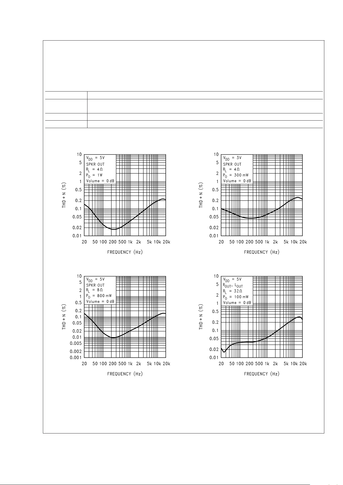
Typical Performance Characteristics
THD+N vs Frequency (LM4851LQ) THD+N vs Frequency (LM4851LQ)
200408B4 200408B5
THD+N vs Frequency THD+N vs Frequency
20040863 20040864
LM4851
www.national.com 6
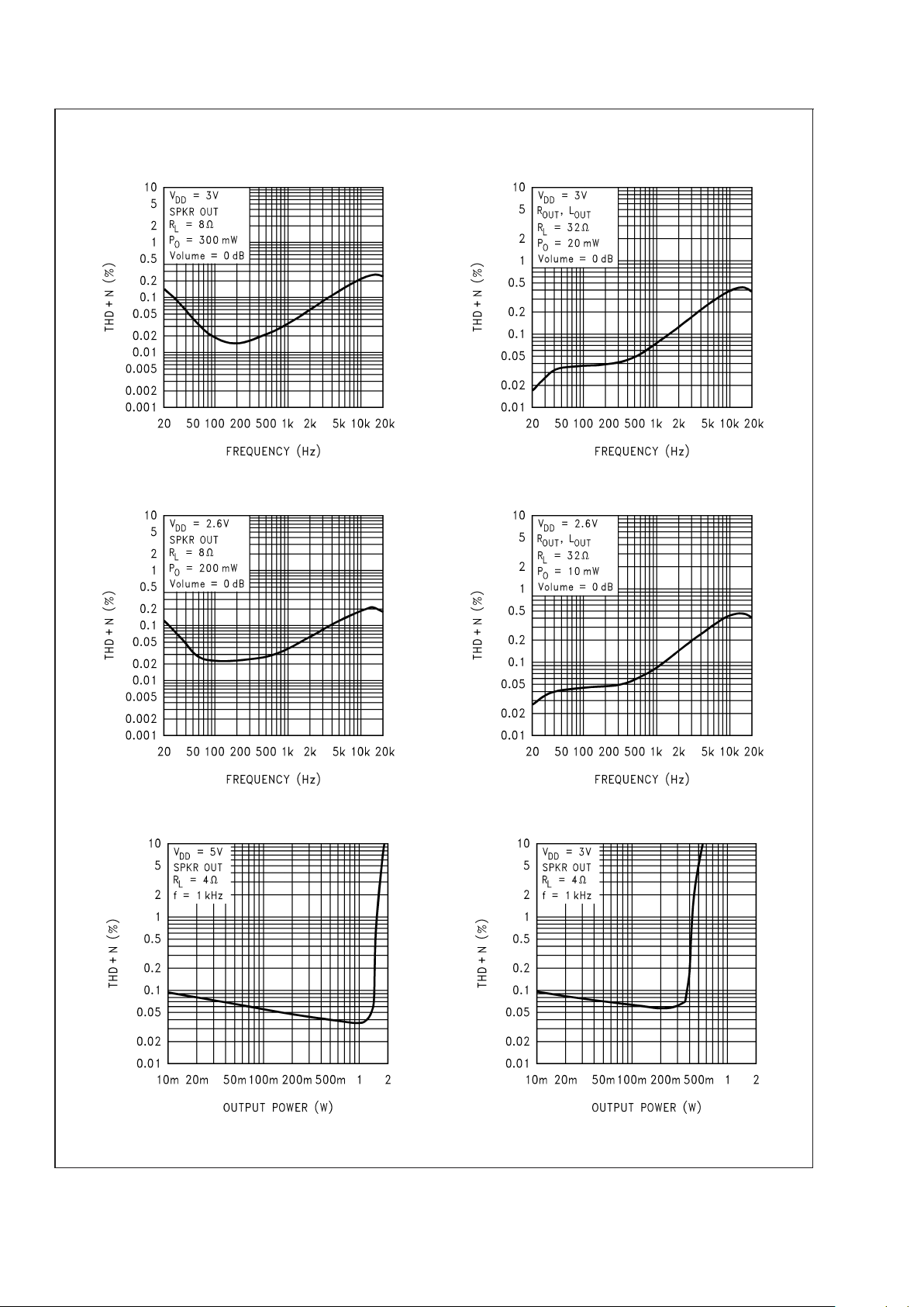
Typical Performance Characteristics (Continued)
THD+N vs Frequency THD+N vs Frequency
20040865 20040866
THD+N vs Frequency THD+N vs Frequency
20040867 20040868
THD+N vs Output Power (LM4851LQ) THD+N vs Output Power (LM4851LQ)
200408B6 200408B7
LM4851
www.national.com7
 Loading...