NSC LM48511 Datasheet
September 2007
LM48511
3W, Ultra-Low EMI, Filterless, Mono, Class D Audio Power
Amplifier with Spread Spectrum
General Description
The LM48511 integrates a boost converter with a high efficiency Class D audio power amplifier to provide 3W continuous power into an 8Ω speaker when operating from a 5V
power supply. When operating from a 3V to 4V power supply,
the LM48511 can be configured to drive 1 to 2.5W into an
8Ω load with less than 1% distortion (THD+N). The Class D
amplifier features a low noise PWM architecture that eliminates the output filter, reducing external component count,
board area consumption, system cost, and simplifying design.
A selectable spread spectrum modulation scheme suppresses RF emissions, further reducing the need for output filters.
The LM48511’s switching regulator is a current-mode boost
converter operating at a fixed frequency of 1MHz. Two selectable feedback networks allow the LM48511 regulator to
dynamically switch between two different output voltages, improving efficiency by optimizing the amplifier’s supply voltage
based on battery voltage and output power requirements.
The LM48511 is designed for use in portable devices, such
as GPS, mobile phones, and MP3 players. The high, 80%
efficiency at 5V, extends battery life when compared to Boosted Class AB amplifiers. Independent regulator and amplifier
shutdown controls optimize power savings by disabling the
regulator when high output power is not required.
The gain of the LM48511 is set by external resistors, which
allows independent gain control from multiple sources by
summing the signals. Output short circuit and thermal overload protection prevent the device from damage during fault
conditions. Superior click and pop suppression eliminates audible transients during power-up and shutdown.
Key Specifications
■ Quiescent Power Supply Current
VDD = 3V
VDD = 5V
9mA (typ)
13.5mA (typ)
■ P
O
at VDD = 5V, PV1 = 7.8V
RL = 8Ω, THD+N = 1%
3.0W (typ)
■ P
O
at VDD = 3V, PV1 = 4.8V
RL = 8Ω, THD+N = 1%
1W (typ)
■ Shutdown Current at V
DD
= 3V
0.01μA (typ)
Features
■
3W Output into 8Ω at 5V with THD+N = 1%
■
Selectable spread spectrum mode reduces EMI
■
80% Efficiency
■
Independent Regulator and Amplifier Shutdown Controls
■
Dynamically Selectable Regulator Output Voltages
■
Filterless Class D
■
3.0V – 5.5V operation
■
Low Shutdown Current
■
Click and Pop Suppression
Applications
■
GPS
■
Portable media
■
Cameras
■
Mobile Phones
■
Handheld games
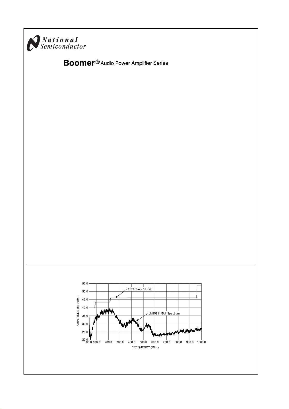
EMI Graph
300222h5
FIGURE 1. LM48511 RF Emissions — 3 inch cable
Boomer® is a registered trademark of National Semiconductor Corporation.
© 2007 National Semiconductor Corporation 300222 www.national.com
LM48511 3W, Ultra-Low EMI, Filterless, Mono, Class D Audio Power Amplifier
with Spread Spectrum
Typical Application
300222i3
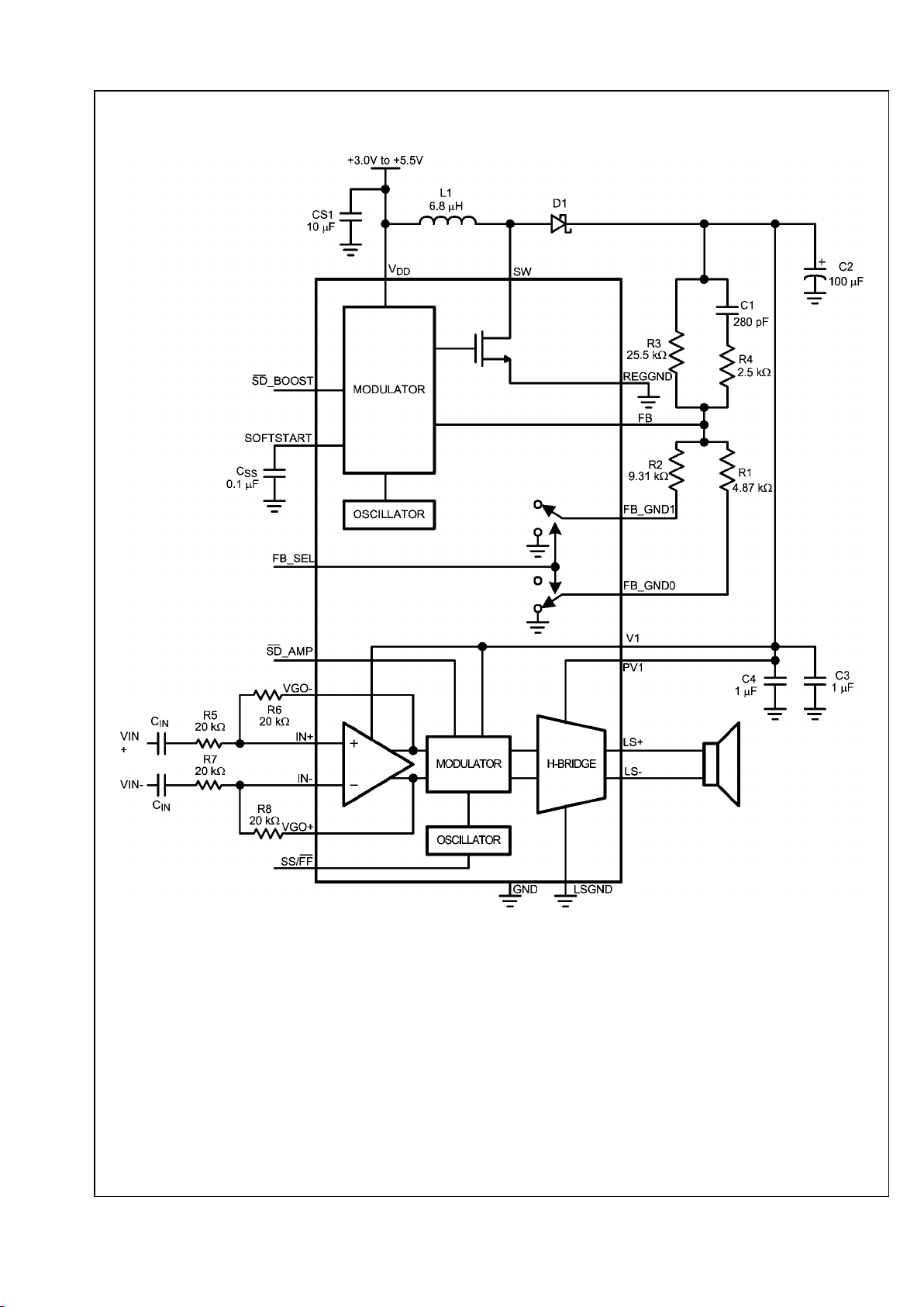
FIGURE 2. Typical LM48511 Audio Amplifier Application Circuit
www.national.com 2
LM48511
Connection Diagrams
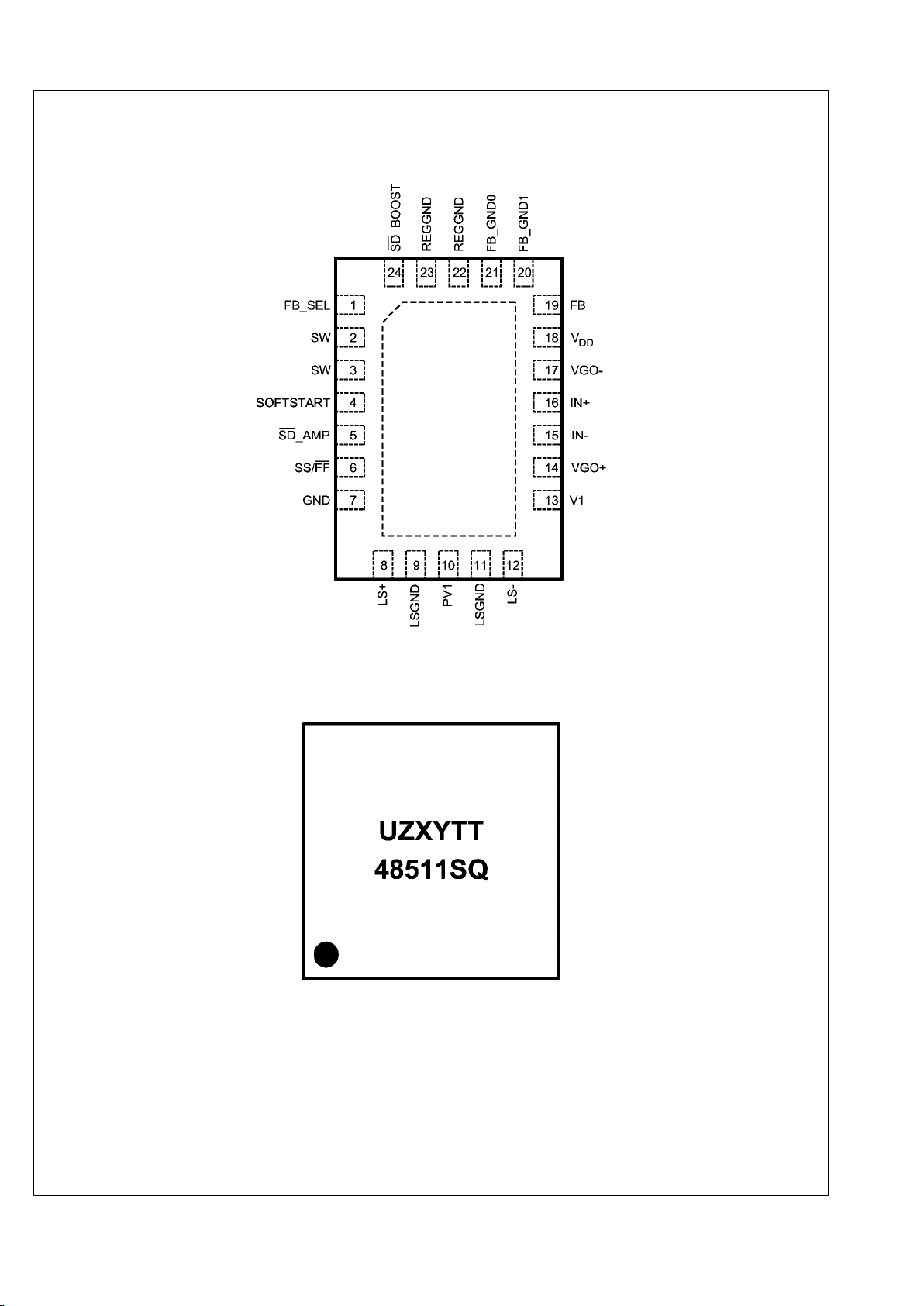
SQ Package
300222d4
Top View
Order Number LM48511SQ
See NS Package Number SQA24B
SQ Package Marking
300222d5
Top View
U — Wafer fab code
Z — Assembly plant
XY — 2 Digit date code
TT — Lot traceability
3 www.national.com
LM48511
Pin Descriptions
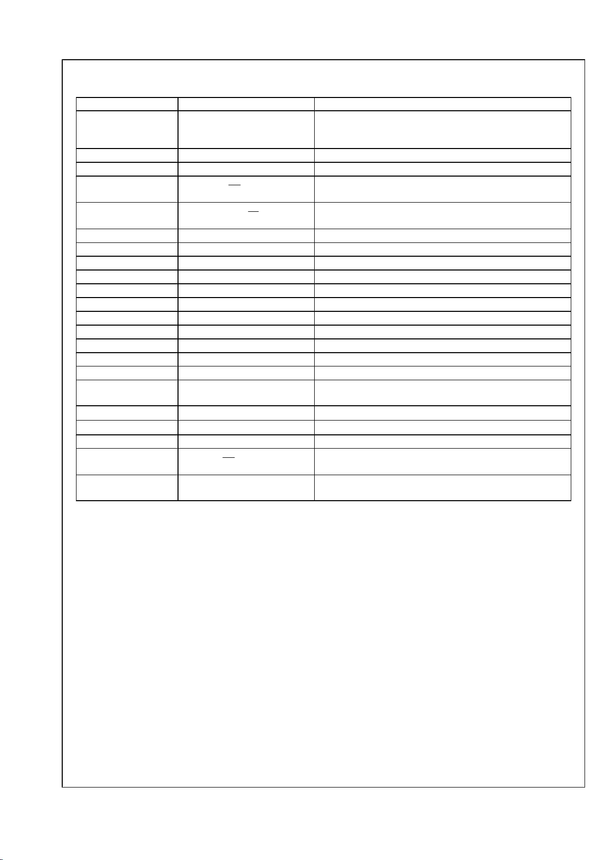
LLP-24 Pin Name Function
1 FB_SEL
Regulator Feedback Select. Connect to VDD to select feedback
network connected to FB_GND1. Connect to GND to select
feedback network connected to FB_GND0.
2,3 SW Drain of the Internal FET Switch
4 SOFTSTART Soft Start Capacitor
5 SD_AMP
Amplifier Active Low Shutdown. Connect to VDD for normal
operation. Connect to GND to disable amplifier.
6 SS/FF
Modulation Mode Select. Connect to VDD for spread spectrum
mode (SS). Connect to GND for fixed frequency mode (FF).
7 GND Signal Ground
8 LS+ Amplifier Non-Inverting Output
9, 11 LSGND Amplifier H-Bridge Ground
10 PV1 Amplifier H-Bridge Power Supply. Connect to V1.
12 LS- Amplifier Inverting Output
13 V1 Amplifier Supply Voltage. Connect to PV1
14 VG0+ Amplifier Non-Inverting Gain Output
15 IN- Amplifier Inverting Input
16 IN+ Amplifier Non-Inverting Input
17 VG0– Amplifier Inverting Gain Output
18 VDD Power Supply
19 FB
Regulator Feedback Input. Connect FB to an external resistive
voltage divider to set the boost output voltage.
20 FB_GND1 Ground return for R3, R1 resistor divider
21 FB_GND0 Ground return for R3, R2 resistor divider
22,23 REGGND Power Ground (Booster)
24 SD_BOOST
Regulator Active Low Shutdown. Connect to VDD for normal
operation. Connect to GND to disable regulator.
DAP
To be soldered to board for enhanced thermal dissipation. Connect
to GND plane.
www.national.com 4
LM48511
Absolute Maximum Ratings (Notes 2, 2)
If Military/Aerospace specified devices are required,
please contact the National Semiconductor Sales Office/
Distributors for availability and specifications.
Supply Voltage (VDD, PV1, V1)
9V
Storage Temperature −65°C to +150°C
Input Voltage
−0.3V to VDD + 0.3V
Power Dissipation (Note 3) Internally limited
ESD Susceptibility (Note 4) 2000V
ESD Susceptibility (Note 5) 200V
Junction Temperature 150°C
Thermal Resistance
θJC (SQ)
3.8°C/W
θJA (SQ)
32.8°C/W
Operating Ratings
Temperature Range
T
MIN
≤ TA ≤ T
MAX
−40°C ≤ TA ≤ +85°C
Supply Voltage (VDD) 3.0V ≤ VDD ≤ 5.5V
Amplifier Voltage (PV1, V1) 4.8V ≤ PV1 ≤ 8.0V
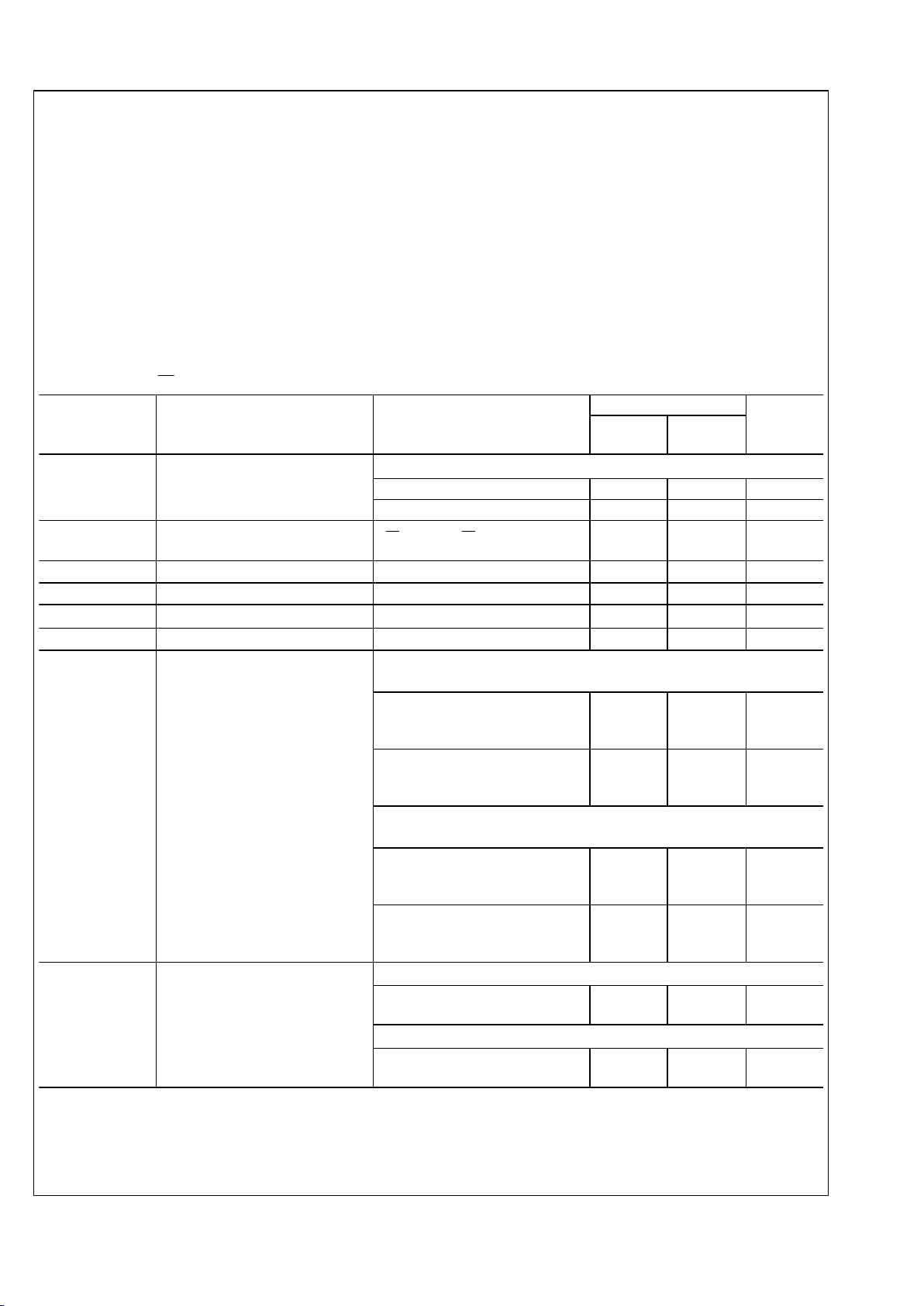
Electrical Characteristics VDD = 5.0V (Notes 1, 2, 11)
The following specifications apply for VDD = 5.0V, PV1 = 7.8V (continuos mode), AV = 2V/V, R3 = 25.5kΩ, RLS = 4.87kΩ, RL =
8Ω, f = 1kHz, SS/FF = GND, unless otherwise specified. Limits apply for TA = 25°C.
Symbol Parameter Conditions
LM48511 Units
(Limits)
Typical
(Note 6)
Limit
(Notes 7, 8)
I
DD
Quiescent Power Supply Current
VIN = 0, R
LOAD
= ∞
Fixed Frequency Mode (FF) 13.5 mA (max)
Spread Spectrum Mode (SS) 14.5 22 mA (max)
I
SD
Shutdown Current
V
SD_BOOST
= V
SD_AMP
= SS =
FB_SEL = GND
0.11 1
μA (max)
V
IH
Logic Voltage Input High
1.03 1.4 V (min)
V
IL
Logic Voltage Input Low
0.92 0.4 V (min)
T
WU
Wake-up Time
CSS = 0.1μF
49 ms
V
OS
Output Offset Voltage Note 12 0.01 3 mV
P
O
Output Power
RL = 8Ω
f = 1kHz, BW = 22kHz
THD+N = 1%
FF
SS
3.0
3.0
2.6 W (min)
W
THD+N = 10%
FF
SS
3.8
3.8
W
W
RL = 4Ω
f = 1kHz, BW = 22kHz
THD+N = 1%
FF
SS
5.4
5.4
W
W
THD+N = 10%
FF
SS
6.7
6.7
W
W
THD+N Total Harmonic Distortion + Noise
PO = 2W, f = 1kHz, RL = 8Ω
FF
SS
0.03
0.03
%
%
PO = 3W, f = 1kHz, RL = 4Ω
FF
SS
0.04
0.05
%
%
5 www.national.com
LM48511
Symbol Parameter Conditions
LM48511 Units
(Limits)
Typical
(Note 6)
Limit
(Notes 7, 8)
ε
OS
Output Noise
f = 20Hz to 20kHz
Inputs to AC GND, No weighting
FF
SS
32
32
µV
RMS
µV
RMS
f = 20Hz to 20kHz
Inputs to AC GND, A weighted
FF
SS
22
22
µV
RMS
µV
RMS
PSRR
Power Supply Rejection Ratio
(Input Referred)
V
RIPPLE
= 200mV
P-P
Sine,
f
RIPPLE =
= 217Hz,
FF
SS
88
87
dB
dB
V
RIPPLE
= 200mV
P-P
Sine,
f
RIPPLE =
= 1kHz,
FF
SS
88
85
dB
dB
V
RIPPLE
= 200mV
P-P
Sine,
f
RIPPLE =
= 10kHz,
FF
SS
77
76
dB
dB
CMRR
Common Mode Rejection Ratio
(Input Referred)
V
RIPPLE
= 1V
P-P
, f
RIPPLE
= 217Hz
73
dB
η
Efficiency
f = 1kHz, RL = 8Ω, PO = 1W
80
%
V
FB
Feedback Pin Reference Voltage 1.23
V
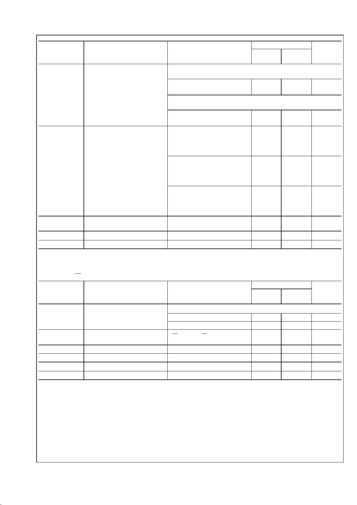
Electrical Characteristics VDD = 3.6V (Notes 1, 2, 11)
The following specifications apply for VDD = 3.6V, PV1 = 7V (continuous mode), AV = 2V/V, R3 = 25.5kΩ, RLS = 5.36kΩ, RL = 8Ω,
f = 1kHz, SS/FF
= GND, unless otherwise specified. Limits apply for TA = 25°C.
Symbol Parameter Conditions
LM48511 Units
(Limits)
Typical
(Note 6)
Limit
(Notes 7, 8)
I
DD
Quiescent Power Supply Current
VIN = 0, R
LOAD
= ∞
Fixed Frequency Mode (FF) 16 mA (max)
Spread Spectrum Mode (SS) 17.5 26.6 mA (max)
I
SD
Shutdown Current
V
SD_BOOST
= V
SD_AMP
= SS =
FB_SEL = GND
0.03 1
μA (max)
V
IH
Logic Voltage Input High
0.96 1.4 V (min)
V
IL
Logic Voltage Input Low
0.84 0.4 V (min)
T
WU
Wake-up Time
CSS = 0.1μF
50 ms
V
OS
Output Offset Voltage Note 12 0.04 mV
www.national.com 6
LM48511

Symbol Parameter Conditions
LM48511 Units
(Limits)
Typical
(Note 6)
Limit
(Notes 7, 8)
P
O
Output Power
RL = 8Ω, f = 1kHz, BW = 22kHz
THD+N = 1%
FF
SS
2.5
2.5
W
W
THD+N = 10%
FF
SS
3.0
3.0
W
W
RL = 4Ω, f = 1kHz, BW = 22kHz
THD+N = 1%
FF
SS
4.3
4.2
W
W
THD+N = 10%
FF
SS
5.4
5.3
W
W
THD+N Total Harmonic Distortion + Noise
PO = 1.5W, f = 1kHz, RL = 8Ω
FF
SS
0.03
0.03
%
%
PO = 3W, f = 1kHz, RL = 4Ω
FF
SS
0.04
0.05
%
%
ε
OS
Output Noise
f = 20Hz to 20kHz
Inputs to AC GND, No weighting
FF
SS
35
36
µV
RMS
µV
RMS
f = 20Hz to 20kHz
Inputs to AC GND, A weighted
FF
SS
25
26
µV
RMS
µV
RMS
PSRR
Power Supply Rejection Ratio
(Input Referred)
V
RIPPLE
= 200mV
P-P
Sine,
f
RIPPLE =
= 217Hz
FF
SS
85
86
dB
dB
V
RIPPLE
= 200mV
P-P
Sine,
f
RIPPLE =
= 1kHz
FF
SS
87
86
dB
dB
V
RIPPLE
= 200mV
P-P
Sine,
f
RIPPLE =
= 10kHz
FF
SS
78
77
dB
dB
CMRR
Common Mode Rejection Ratio
(Input Referred)
V
RIPPLE
= 1V
P-P
, f
RIPPLE
= 217Hz
73
dB
η
Efficiency
f = 1kHz, RL = 8Ω, PO = 1W
77
%
V
FB
Feedback Pin Reference Voltage 1.23
V
7 www.national.com
LM48511
 Loading...