

LM48510
Boosted Class D Audio Power Amplifier
LM48510 Boosted Class D Audio Power Amplifier
March 2007
General Description
The LM48510 integrates a boost converter with a high efficiency mono, Class D audio power amplifier to provide 1.2W
continuous power into an 8Ω speaker when operating on a
3.3V power supply with boost voltage (PV1) of 5.0V. When
operating on a 3.3V power supply, the LM48510 is capable of
driving a 4Ω speaker load at a continuous average output of
1.7W with less than 1% THD+N. The Class D amplifier is a
low noise, filterless PWM architecture that eliminates the output filter, reducing external component count, board area
consumption, system cost, and simplifying design.
The LM48510's switching regulator is a current-mode boost
converter operating at a fixed frequency of 0.6MHz.
The LM48510 is designed for use in mobile phones and other
portable communication devices. The high (76%) efficiency
extends battery life when compared to Boosted Class AB amplifiers. The LM48510 features a low-power consumption
shutdown mode. Shutdown may be enabled by driving the
Shutdown pin to a logic low (GND).
The gain of the Class D is externally configurable which allows
independent gain control from multiple sources by summing
the signals. Output short circuit and Thermal shutdown protection prevent the device from damage during fault conditions. Superior click and pop suppression eliminates audible
transients during power-up and shutdown.
Key Specifications
■ Quiescent Power Supply Current 6mA (typ)
■ Output Power
(RL = 8Ω, THD+N ≤ 1%,
VDD = 3.3V, PV1 = 5.0V)
■ Shutdown Current
1.2W (typ)
0.01μA (typ)
Features
Click and Pop Suppression
■
Low 0.01μA Shutdown Current
■
76% Efficiency
■
Filterless Class D
■
2.7V - 5.0V operation (VDD)
■
Externally configurable gain on Class D
■
Very fast turn on time: 17μs
■
Independent Boost and Amplifier shutdown pins
■
Applications
Mobile Phones
■
PDAs
■
Portable media
■
Cameras
■
Handheld games
■
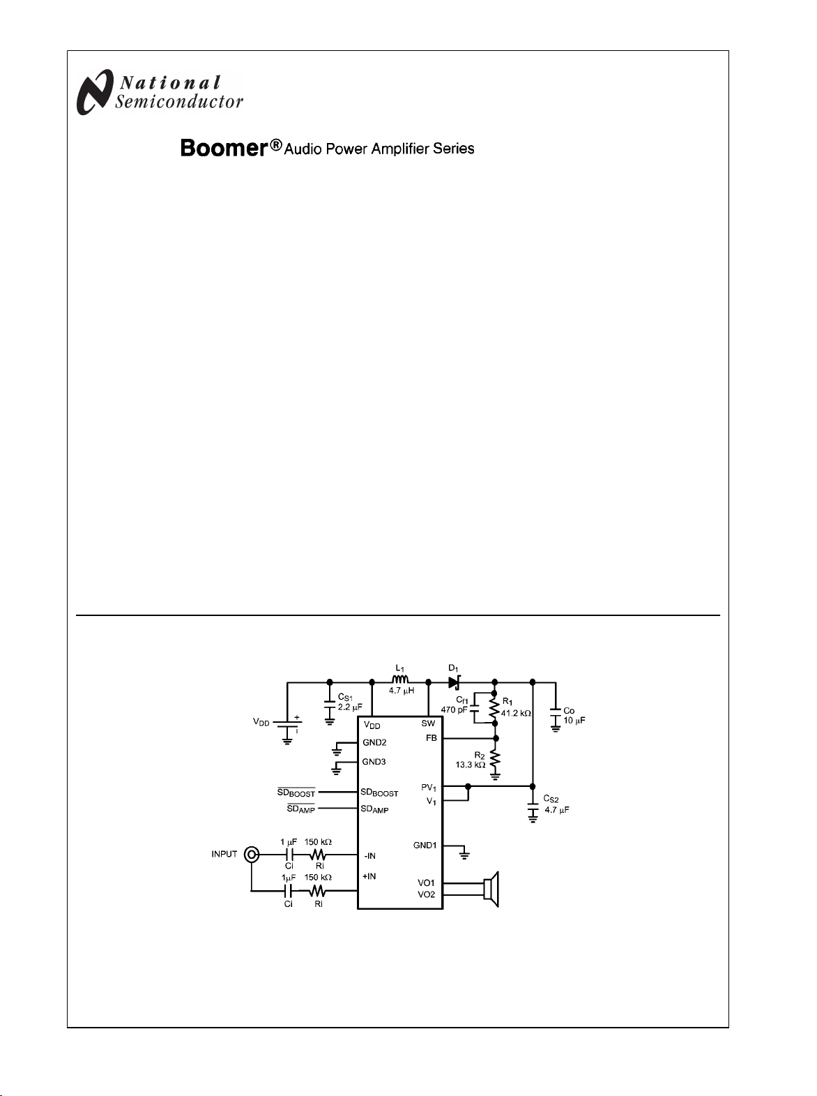
Typical Application
20123266
FIGURE 1. Typical LM48510 Audio Amplifier Application Circuit
Boomer® is a registered trademark of National Semiconductor Corporation.
© 2007 National Semiconductor Corporation 201232 www.national.com
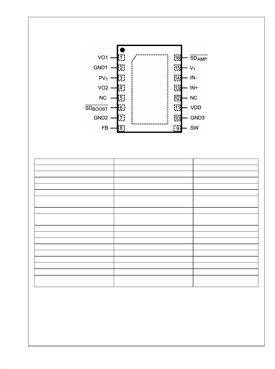
Connection Diagram
LM48510
LM48510SD
Top View
20123267
Order Number LM48510SD
See NS Package Number SDA16B
LLP-14 Pin Name Function
1 VO1 Amplifier Output
2 GND1 Ground
3 PV1 Amplifier Power Input
4 VO2 Amplifier Output
5 NC1 No Connect
6 SD
BOOST
Boost Regulator Active Low
Shutdown
7 GND2 Signal Ground (Booster)
8 FB Feedback point that connects to
external resistive divider
9 SW Drain of the Internal FET Switch
10 GND3 Power Ground (Booster)
11 VDD Power Supply
12 NC2 No Connect
13 IN+ Amplifier Non-Inverting Input
14 IN- Amplifier Inverting Input
15 V1 Amplifier Power Input
16 SD
DAP
AMP
To be soldered to board for
Amplifier Active Low Shutdown
enhanced thermal dissipation.
www.national.com 2
LM48510
Absolute Maximum Ratings (Notes 2, 2)
If Military/Aerospace specified devices are required,
please contact the National Semiconductor Sales Office/
Thermal Resistance
θJA (SD)
37°C/W
See AN-1187 'Leadless Leadframe Packaging (LLP)'
Distributors for availability and specifications.
Supply Voltage (VDD, V1)
6V
Storage Temperature −65°C to +150°C
Input Voltage
−0.3V to VDD + 0.3V
Power Dissipation (Note 3) Internally limited
ESD Susceptibility (Note 4) 2000V
ESD Susceptibility (Note 5) 200V
Operating Ratings
Temperature Range
T
≤ TA ≤ T
MIN
MAX
Supply Voltage (VDD) 2.7V ≤ VDD ≤ 5.0V
Supply Voltage (V1) 4.5V ≤ V1 ≤ 5.5V
−40°C ≤ TA ≤ +85°C
Junction Temperature 150°C
Electrical Characteristics VDD = 3.3V (Notes 1, 2)
The following specifications apply for VDD = 3.3V, PV1 = V1 = 5.0V, AV = 6dB (Ri = 150kΩ), RL = 15µH + 8Ω +15µH, fIN = 1kHz,
unless otherwise specified. Limits apply for TA = 25°C.
Symbol Parameter Conditions LM48510 Units
I
I
V
V
T
V
P
DD
SD
SDIH
SDIL
WU
OS
O
Quiescent Power Supply Current
Shutdown Current
Shutdown Voltage Input High
Shutdown Voltage Input Low
Wake-up Time 17
Output Offset Voltage 10 mV
Output Power
THD+N Total Harmonic Distortion + Noise
VIN = 0, R
SD
AMP
LOAD
= SD
= ∞
BOOST
= GND
(Note 9)
SD1 Boost
SD2 Amplifier
SD1 Boost
SD2 Amplifier
RL = 15μH + 4Ω + 15μH
THD+N = 1% (max),
f = 1kHz, 22kHz, BW
VDD = 3.3V
RL = 15μH + 8Ω + 15μH
THD+N = 1% (max),
f = 1kHz, 22kHz, BW
VDD = 3.3V
RL = 15μH + 4Ω + 15μH
THD+N = 10% (max),
f = 1kHz, 22kHz, BW
VDD = 2.7V
VDD = 3.3V
RL = 15μH + 8Ω + 15μH
THD+N = 10% (max),
f = 1kHz, 22kHz, BW
VDD = 2.7V
VDD = 3.3V
PO = 500mW, f = 1kHz,
RL = 15μH + 8Ω + 15μH,
VDD = 2.7V
PO = 500mW, f = 1kHz,
RL = 15μH + 8Ω + 15μH,
VDD = 3.3V
Typical
(Note 6)
6.06 8.75 mA (max)
0.01 1
1.7
1.2 0.9 W (min)
1.11
1.9
0.98
1.55
0.06 %
0.07
Limit
(Notes 7, 8)
1.5
1.4
0.5
0.4
(Limits)
μA (max)
V (min)
V (min)
V (max)
V (max)
μs
W
W
W
W
W
%
3 www.national.com
Symbol Parameter Conditions LM48510 Units
LM48510
ε
OS
Output Noise
VDD = 3.3V, f = 20Hz – 20kHz
Inputs to AC GND, No weighting
input referred
VDD = 3.3V, f = 20Hz – 20kHz
Inputs to AC GND, A weighted
Typical
(Note 6)
67
47
Limit
(Notes 7, 8)
input referred
A
V
Gain
PSRR Power Supply Rejection Ratio
CMRR Common Mode Rejection Ratio
η
V
FB
Note 1: All voltages are measured with respect to the GND pin, unless otherwise specified.
Note 2: Absolute Maximum Ratings indicate limits beyond which damage to the device may occur. Operating Ratings indicate conditions for which the device is
functional, but do not guarantee specific performance limits. Electrical Characteristics state DC and AC electrical specifications under particular test conditions
which guarantee specific performance limits. This assumes that the device is within the Operating Ratings. Specifications are not guaranteed for parameters
where no limit is given, however, the typical value is a good indication of device performance.
Note 3: The maximum power dissipation must be derated at elevated temperatures and is dictated by T
allowable power dissipation is P
Note 4: Human body model, 100pF discharged through a 1.5kΩ resistor.
Note 5: Machine Model, 220pF–240pF discharged through all pins.
Note 6: Typicals are measured at 25°C and represent the parametric norm.
Note 7: Limits are guaranteed to National's AOQL (Average Outgoing Quality Level).
Note 8: Datasheet min/max specification limits are guaranteed by design, test, or statistical analysis.
Note 9: Shutdown current is measured with components R1 and R2 removed.
Note 10: Feedback pin reference voltage is measured with the Audio Amplifier disconnected from the Boost converter (the Boost converter is unloaded).
Efficiency
Feedback Pin Reference Voltage (Note 10) 1.24
= (T
DMAX
− TA) / θJA or the given in Absolute Maximum Ratings, whichever is lower.
JMAX
V
RIPPLE
f
RIPPLE =
V
RIPPLE
f
RIPPLE =
V
RIPPLE
f
RIPPLE =
V
RIPPLE
= 200mV
= 217Hz
= 200mV
= 1kHz
= 200mV
= 10kHz
= 1V
P-P
P-P
P-P
P-P
, f
RIPPLE
Sine,
Sine,
Sine,
= 217Hz
PO = 1W, f = 1kHz,
RL = 15μH + 8Ω + 15μH, VDD = 3.3V
, θJA, and the ambient temperature, TA. The maximum
JMAX
300kΩ/R
i
89 dB
83
55
70
76
(Limits)
µV
RMS
µV
RMS
V/V
dB
dB
dB
%
V
www.national.com 4
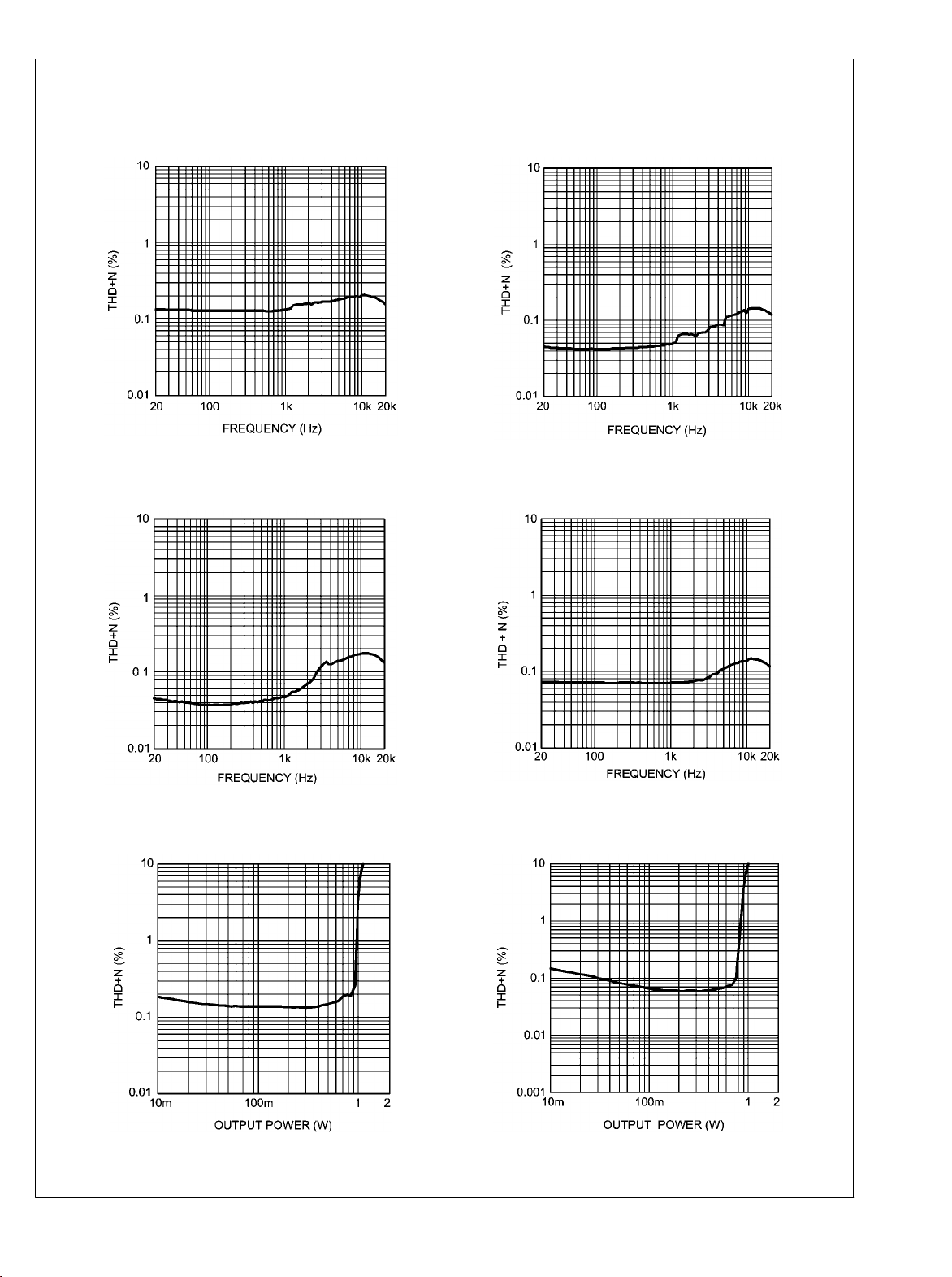
Typical Performance Characteristics
LM48510
THD+N vs Frequency
VDD = 2.7V, RL = 15μH + 4Ω + 15μH
THD+N vs Frequency
VDD = 3.3V, RL = 15μH + 4Ω + 15μH
20123237
THD+N vs Frequency
VDD = 2.7V, RL = 15μH + 8Ω + 15μH
20123250
THD+N vs Frequency
VDD = 3.3V, RL = 15μH + 8Ω + 15μH
THD+N vs Output Power
VDD = 2.7V, RL = 15μH + 4Ω + 15μH
20123239
20123241
20123240
THD+N vs Output Power
VDD = 2.7V, RL = 15μH + 8Ω + 15μH
20123251
5 www.national.com
LM48510
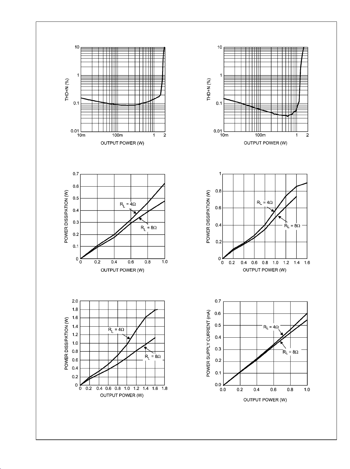
THD+N vs Output Power
VDD = 3.3V, RL = 15μH + 4Ω + 15μH
THD+N vs Output Power
VDD = 3.3V, RL = 15μH + 8Ω + 15μH
Power Dissipation vs Output Power
VDD = 2.7V
Power Dissipation vs Output Power
VDD = 4.2V
20123243
20123234
20123244
Power Dissipation vs Output Power
VDD = 3.3V
20123235
Power Supply Current vs Output Power
VDD = 2.7V
20123236
www.national.com 6
20123229
 Loading...