

NSC LM4850MM, LM4850LDX, LM4850LD, LM4850MWC, LM4850MTX Datasheet
...
LM4850
Mono 1.5 W / Stereo 300 mW Power Amplifier
General Description
The LM4850 is an audio power amplifier capable of delivering 1.5W (typ) of continuous average power into a mono 4Ω
bridged-tied load (BTL) with 1% THD+N or 95mW per channel of continuous average power into stereo 32Ω
single-ended (SE) loads with 1% THD+N, using a 5V power
supply.
The LM4850 can automatically switch between mono BTL
and stereo SE modes utilizing a headphone sense pin. It is
ideal for any system that provides both a monaural speaker
output and a stereo line or headphone output
Boomer audio power amplifiers were designed specifically to
provide high quality output power with a minimal amount of
external components. Since the LM4850 does not require
bootstrap capacitors or snubber networks, it is optimally
suited for low-power portable systems.
The LM4850 features an externally controlled, micropower
consumption shutdown mode and thermal shutdown protection. The unity-gain stable LM4850’s gain is set by external
gain-setting resistors
Note 1: An LM4850LD that has been properly mounted to a circuit board will
deliver 1.9W into 3Ω (at 1% THD+N). The other package options for the
LM4850 will deliver 1.1W into 8Ω (at 1% THD+N). See Application Infor-
mation sections for further information concerning the LM4850LD,
LM4850MM, and LM4850MT.
Key Specifications
n Output Power at 1% THD+N, 1kHz:
n LM4850LD 3Ω BTL 1.9W (typ)
n LM4850LD 4Ω BTL 1.7W (typ)
n LM4850MM, MT 4Ω BTL 1.5W (typ)
n LM4850LD, MM, MT 8Ω BTL 1.1W (typ)
n LM4850LD, MM, MT 8Ω SE 300mW (typ)
n LM4850LD, MM, MT 32Ω SE 95mW (typ)
n THD+N at 1kHz, 95mW into 32Ω SE 1% (typ)
n Single Supply Operation 2.4 to 5.5V
n Shutdown Current 44µA (typ)
Features
n Mono 1.5W BTL or stereo 300mW output
n Headphone sense
n “Click and pop” suppression circuitry
n No bootstrap capacitors required
n Thermal shutdown protection
n Unity-gain stable
n LLP, TSSOP, and MSOP packaging
Applications
n Portable computers
n Desktop computers
n PDA’s
n Handheld games
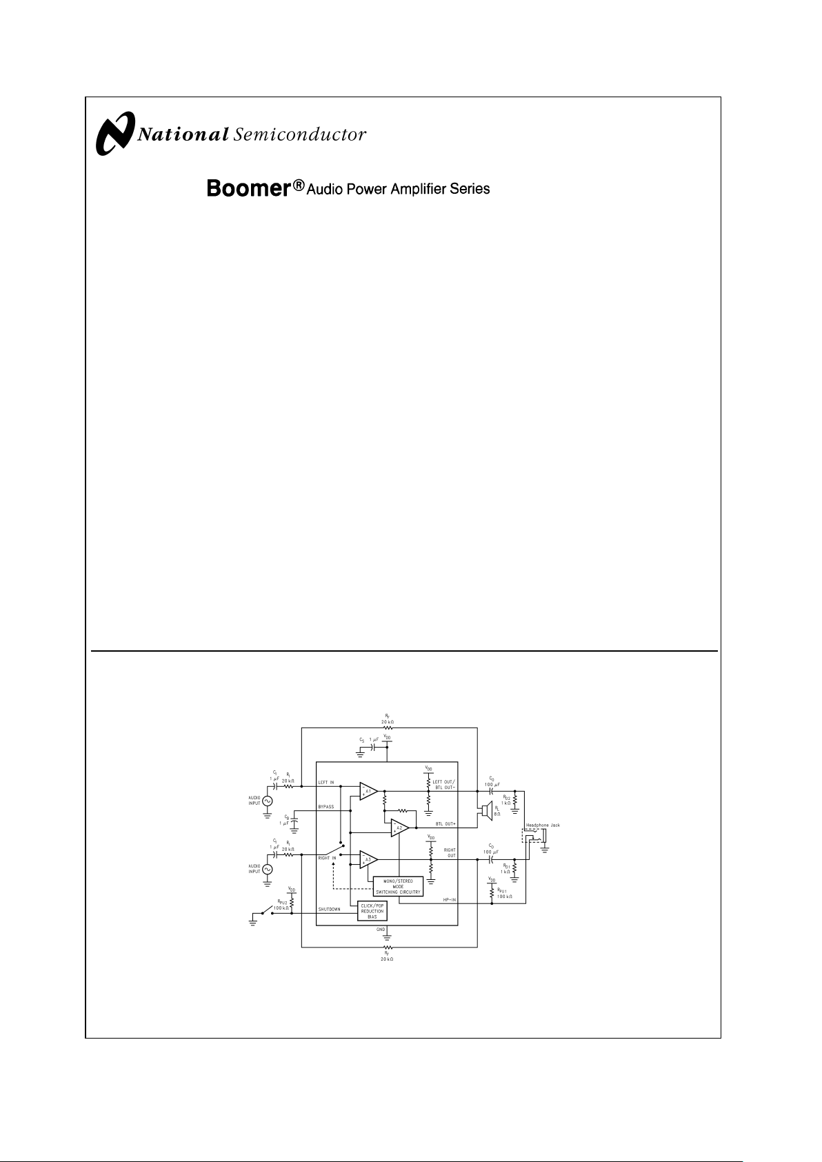
Typical Application
Boomer®is a registered trademark of National Semiconductor Corporation.
20001031
FIGURE 1. Typical Audio Amplifier Application Circuit
July 2002
LM4850 Mono 1.5 W / Stereo 300 mW Power Amplifier
© 2002 National Semiconductor Corporation DS200010 www.national.com
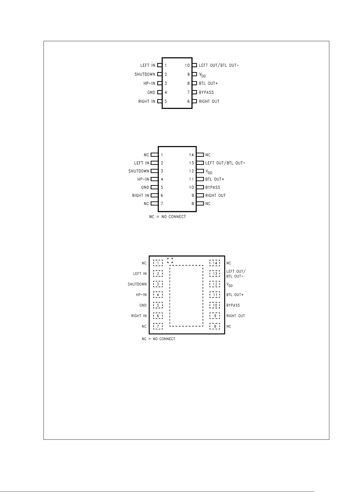
Connection Diagrams
20001051
Top View
10 Lead MSOP
Order Number LM4850MM
See NS Package Number MUB10A
20001052
Top View
14 Lead TSSOP
Order Number LM4850MT
See NS Package Number MTC14
20001002
Top View
14 Lead LLP
Order Number LM4850LD
See NS Package Number LDA14A
LM4850
www.national.com 2
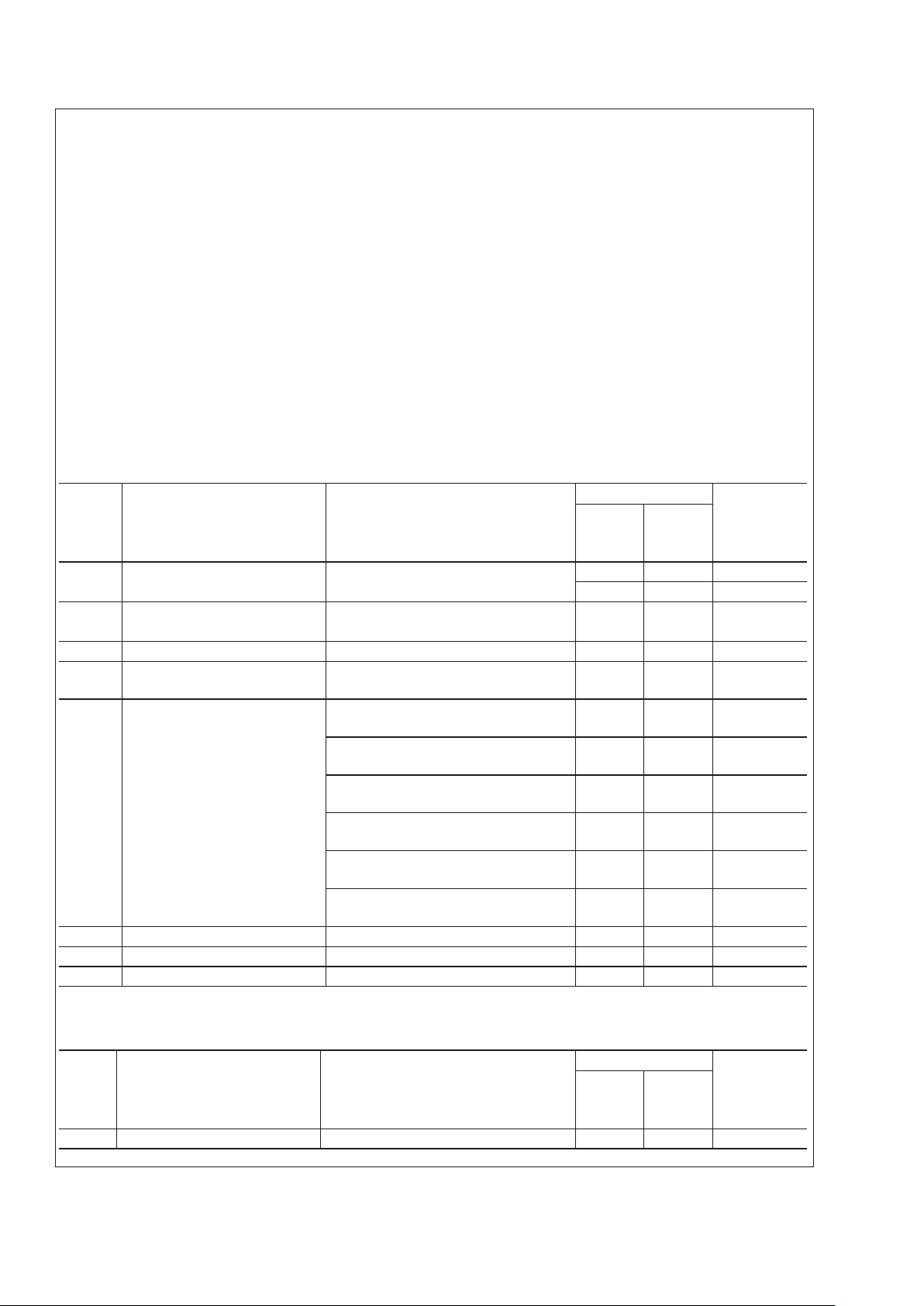
Absolute Maximum Ratings (Note 3)
If Military/Aerospace specified devices are required,
please contact the National Semiconductor Sales Office/
Distributors for availability and specifications.
Supply Voltage 6.0V
Storage Temperature −65˚C to +150˚C
ESD Susceptibility (Note 5) 3.5kV
ESD Machine model (Note 8) 250V
Junction Temperature (T
J
) 150˚C
Solder Information (Note 2)
Small Outline Package
Vapor Phase (60 sec.) 215˚C
Infrared (15 sec.) 220˚C
Thermal Resistance
θ
JA
(typ) —MUB10A 194˚C/W
θ
JC
(typ) — MUB10A 52˚C/W
θ
JA
(typ) — MTC14 150˚C/W
θ
JC
(typ) — MTC14 40˚C/W
θ
JA
(typ) — LDA14A (Note 10) 56˚C/W
θ
JC
(typ) — LDA14A 4.3˚C/W
Operating Ratings (Note 3)
Temperature Range
−40˚C ≤ to 85˚C
Supply Voltage V
DD
2.4V ≤ VDD≤ 5.5V
Note 2: See AN-450 ’Surface Mounting and their effects on Product Reliability’ for other methods of soldering surface mount devices.
Electrical Characteristics (Notes 3, 9)
The following specifications apply for VDD= 5.0V, TA= 25˚C unless otherwise specified.
Symbol Parameter Conditions LM4850 Units
(Limits)
Typical
(Note 6)
Limit
(Note 7)
V
DD
Supply Voltage 2.4 V (min)
5.5 V (max)
I
DD
Supply Current BTL Mode; VIN= 0V; IO= 0A 2.4 7.0 mA
SE Mode; V
IN
= 0V; IO= 0A 2.4 7.0 mA
I
SD
Shutdown Current SD Mode 44 µA
V
OS
Output Offset Voltage BTL Mode; AV=2
BTL OUT+ to BTL OUT−
5.0 40 mV
P
O
Output Power LM4850LD; BTL Mode; RL=3Ω
THD+N = 1% (Note 11)
1.9 W
LM4850LD; BTL Mode; RL=4Ω
THD+N = 1% (Note 11)
1.7 W
LM4850MT, MM; BTL Mode; R
L
=4Ω
THD+N = 1%
1.5 W
BTL Mode; R
L
=8Ω
THD+N = 1%
1.1 W
SE Mode; RL=8Ω
THD+N = 1%
300 mW
SE Mode; R
L
=32Ω
THD+N = 1%
95 mW
V
IH
Shutdown Input Voltage High Is<80µA 2.0 V (min)
V
IL
Shutdown Input Voltage Low Is>0.5mA 0.8 V (max)
Crosstalk Channel Seperation SE Mode, R
L
=32Ω; f = 1kHz 73 dB
Electrical Characteristics (Notes 3, 9)
The following specifications apply for VDD= 3.3V, TA= 25˚C unless otherwise specified.
Symbol Parameter Conditions LM4850 Units
(Limits)
Typical
(Note 6)
Limit
(Note 7)
I
DD
Supply Current BTL Mode; VIN= 0V; IO= 0A 2.0 mA
LM4850
www.national.com3
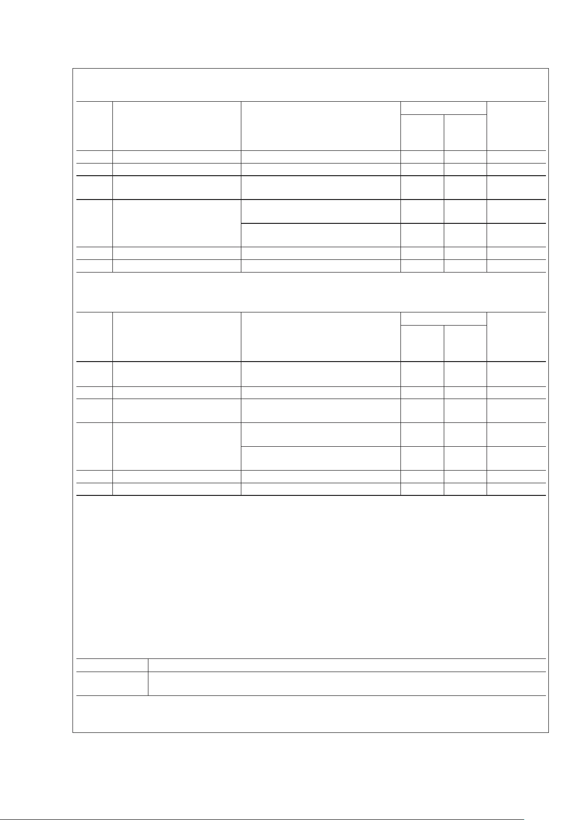
Electrical Characteristics (Notes 3, 9) (Continued)
The following specifications apply for VDD= 3.3V, TA= 25˚C unless otherwise specified.
Symbol Parameter Conditions LM4850 Units
(Limits)
Typical
(Note 6)
Limit
(Note 7)
SE Mode; V
IN
= 0V; IO= 0A 2.0 mA
I
SD
Shutdown Current SD Mode 30 µA
V
OS
Output Offset Voltage BTL Mode; AV=2
BTL OUT+ to BTL OUT−
5.0 40 mV
P
O
Output Power BTL Mode; RL=8Ω
THD+N = 1%
440 mW
SE Mode; R
L
=32Ω
THD+N = 1%
40 mW
V
IH
Shutdown Input Voltage High Is<80µA 2.0 V (min)
V
IL
Shutdown Input Voltage Low Is>0.5mA 0.8 V (max)
Electrical Characteristics(Notes 3, 9)
The following specifications apply for VDD= 2.7V, TA= 25˚C unless otherwise specified.
Symbol Parameter Conditions LM4850 Units
(Limits)
Typical
(Note 6)
Limit
(Note 7)
I
DD
Supply Current BTL Mode; VIN= 0V; IO= 0A 1.8 mA
SE Mode; V
IN
= 0V; IO= 0A 1.8 mA
I
SD
Shutdown Current SD Mode 25 µA
V
OS
Output Offset Voltage BTL Mode; AV=2
BTL OUT+ to BTL OUT−
5.0 40 mV
P
O
Output Power BTL Mode; RL=8Ω
THD+N = 1%
300 mW
SE Mode; R
L
=32Ω
THD+N = 1%
25 mW
V
IH
Shutdown Input Voltage High Is<80 µA 2.0 V (min)
V
IL
Shutdown Input Voltage Low Is>0.5mA 0.8 V (max)
Note 3: Absolute Maximum Rating indicate limits beyond which damage to the device may occur.
Note 4: Operating Ratings indicate conditions for which the device is functional, but do not guarantee specific performance limits. For guaranteed specifications and
test conditions, see the Electrical Characteristics. The guaranteed specifications apply only for the test conditions listed. Some performance characteristics may
degrade when the device is not operated under the listed test conditions.
Note 5: Human body model, 100pF discharged through a 1.5kΩ resistor.
Note 6: Typical specifications are specified at +25˚C and represent the most likely parametric norm.
Note 7: Datasheet min/max specification limits are guaranteed by design, test, or statistical analysis.
Note 8: Machine Model ESD test is covered by specification EIAJ IC-121-1981. A 200pF cap is charged to the specified voltage, then discharged directly into the
IC with no external series resistor (resistance of discharge path must be under 50Ω).
Note 9: All voltages are measured with respect to the ground pin, unless otherwise specified.
Note 10: The given θ
JA
is for a LM4850LD with the Exposed-DAP soldered to an exposed 1in2area of 1oz printed circuit board copper.
Note 11: When driving 3Ω or 4Ω loads from a 5V supply, the LM4850 must be mounted to a circuit board.
Note 12: Limits are guaranteed to National’s AOQL ( Average Outgoing Quality Level ).
External Components Description
(Refer to Figure 1.)
Components Functional Description
1. R
i
Inverting input resistance which sets the closed-loop gain in conjunction with Rf. This resistor also forms a
high pass filter with C
i
at fc= 1/(2πRiCi).
LM4850
www.national.com 4
External Components Description (Continued)
(Refer to Figure 1.)
Components Functional Description
2. C
i
Input coupling capacitor which blocks the DC voltage at the amplifier’s input terminals. Also creates a
highpass filter with R
i
at fc= 1/(2πRiCi). Refer to the section, Proper Selection of External Components,
for an explanation of how to determine the value of C
i
.
3. R
f
Feedback resistance which sets the closed-loop gain in conjunction with Ri.
4. C
s
Supply bypass capacitor which provides power supply filtering. Refer to the Power Supply Bypassing
section for information concerning proper placement and selection of the supply bypass capacitor.
5. C
B
Bypass pin capacitor which provides half-supply filtering. Refer to the section, Proper Selection of
External Components, for information concerning proper placement and selection of C
B
.
6. C
O
Output coupling capacitor which blocks the DC voltage at the amplifier’s output. Forms a high pass filter
with the single-ended load R
L
at fO= 1/(2π RLCO).
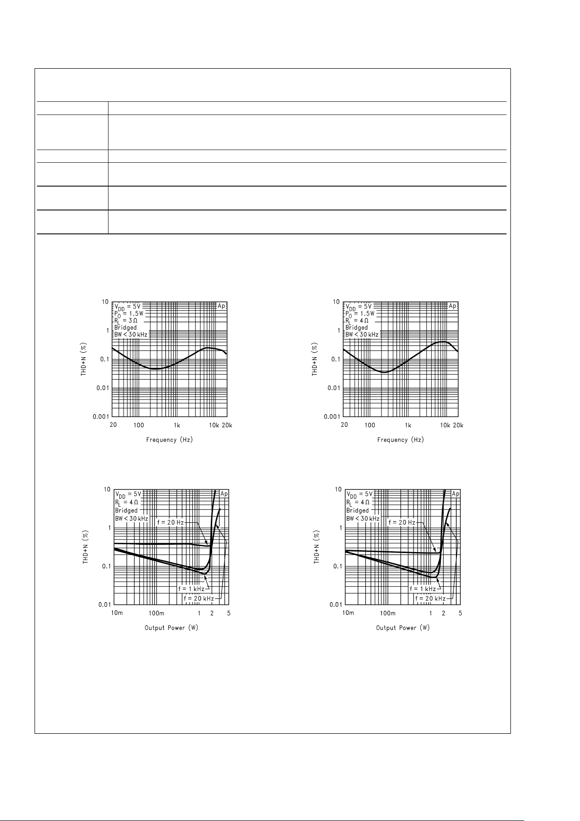
Typical Performance Characteristics
LD Specific Characteristics
LM4850LD
THD+N vs Frequency
LM4850LD
THD+N vs Frequency
20001075 20001076
LM4850LD
THD+N vs Output Power
LM4850LD
THD+N vs Output Power
20001077 20001078
LM4850
www.national.com5
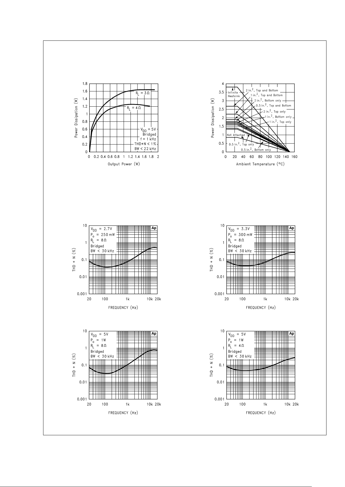
Typical Performance Characteristics
LD Specific Characteristics
(Continued)
LM4850LD
Power Dissipation vs Output Power
LM4850LD (Note 13)
Power Derating Curve
20001079
20001094
Note 13: This curve shows the LM4850LD’s thermal dissipation ability at different ambient temperatures given the exposed-DAP of the part is soldered to a plane
of 1oz. Cu with an area given in the label of each curve. This label also designated whether the plane exists on the same (top) layer as the chip, on the bottom layer,
or on both layers. Infinite heatsink and unattached (no heatsink) conditions are also shown.
Typical Performance Characteristics
Non-LD Specific Characteristics
THD+N vs Frequency THD+N vs Frequency
20001063 20001064
THD+N vs Frequency THD+N vs Frequency
20001065 20001066
LM4850
www.national.com 6
 Loading...