

LM4841
Stereo 2W Amplifiers with DC Volume Control,
Transient Free Outputs, and Cap-less Headphone Drive
General Description
The LM4841 is a monolithic integrated circuit that provides
DC volume control and stereo bridged audio power amplifiers capable of producing 2W into 4Ω (Note 1) or 2.2W into
3Ω (Note 2) with less than 1.0% THD.
The LM4841 uses advanced, latest generation circuitry to
eliminate all traces of clicks and pops when the supply
voltages is first applied. The amplifier has a headphoneamplifier-select input pin that is used to switch the amplifiers
from bridge to single-ended mode for driving headphones. A
new circuit topology eliminates headphone output coupling
capacitors (patent pending).
Boomer
®
audio integrated circuits are designed specifically
to provide high quality audio while requiring a minimum
amount of external components. The LM4841 incorporates a
DC volume control, stereo bridged audio power amplifiers
and a selectable gain or bass boost, making it optimally
suited for multimedia monitors, portable radios, desktop, and
portable computer applications.
The LM4841 features an externally controlled, low-power
consumption shutdown mode (Shutdown Low), and both a
power amplifier and headphone mute for maximum system
flexibility and performance.
Note 1: When properly mounted to the circuit board, LM4841MH and
LM4841LQ will deliver 2W into 4Ω. The LM4841MT will deliver 1.1W into 8Ω.
See the Application Information section for LM4841MH usage information.
Note 2: An LM4841MH that has been properly mounted to the circuit board
and forced-air cooled will deliver 2.2W into 3Ω.
Key Specifications
n POat 1% THD+N
n into 3Ω (MH and LQ) 2.2W (typ)
n into 4Ω ( MH and LQ) 2.0W (typ)
n into 8Ω (MT, MH, and LQ) 1.1W (typ)
n Single-ended THD+N at 85mW into 32Ω 1.0%(typ)
n Shutdown current 0.7µA (typ)
Features
n Stereo headphone amplifier mode that eliminates the
Output Coupling Capacitors (patent pending)
n Acoustically Enhanced DC Volume Control Taper
n System Beep Detect
n Stereo switchable bridged/single-ended power amplifiers
n Selectable internal/external gain and bass boost
n Advanced “click and pop” suppression circuitry
n Thermal shutdown protection circuitry
Applications
n Portable and Desktop Computers
n Multimedia Monitors
n Portable Radios, PDAs, and Portable TVs
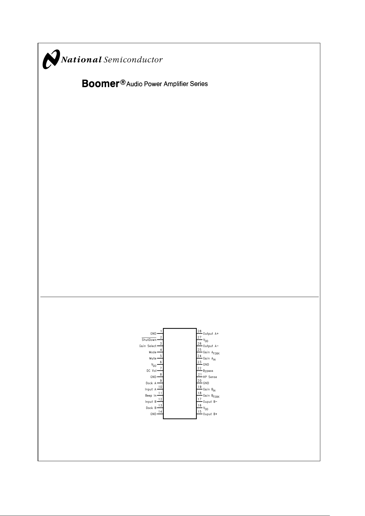
Connection Diagrams
TSSOP Package
20028002
Top View
Order Number LM4841MT or LM4841MH
See NS Package Number MTC28 for TSSOP and MXA28A for Exposed-DAP TSSOP
Boomer®is a registered trademark of National Semiconductor Corporation.
August 2002
LM4841 Stereo 2W Amplifiers with DC Volume Control,Transient Free Outputs, and Cap-less
Headphone Drive
© 2002 National Semiconductor Corporation DS200280 www.national.com
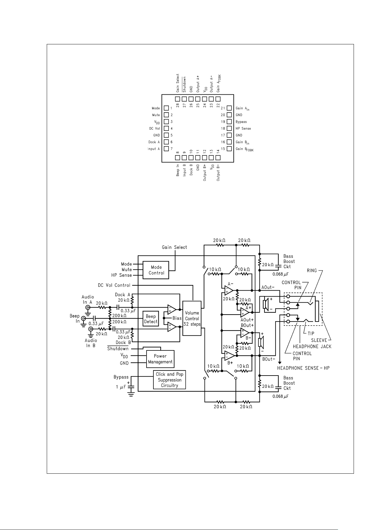
Connection Diagrams (Continued)
LLP Package
20028097
Top View
Order Number LM4841LQ
See NS Package Number LQA028AA for Exposed-DAP LLP
Block Diagram
20028001
FIGURE 1. LM4841 Block Diagram
LM4841
www.national.com 2
Absolute Maximum Ratings (Note 10)
If Military/Aerospace specified devices are required,
please contact the National Semiconductor Sales Office/
Distributors for availability and specifications.
Supply Voltage 6.0V
Storage Temperature -65˚C to +150˚C
Input Voltage −0.3V to V
DD
+0.3V
Power Dissipation (Note 11) Internally limited
ESD Susceptibility (Note 12)
All pins except Pin 28 2500V
Pin 28 6500V
ESD Susceptibility (Note 13) 200V
Junction Temperature 150˚C
Soldering Information
Small Outline Package
Vapor Phase (60 sec.) 215˚C
Infrared (15 sec.) 220˚C
See AN-450 “Surface Mounting and their Effects on
Product Reliability” for other methods of soldering surface
mount devices.
θ
JC
(typ) — LQA028A 3˚C/W
θ
JA
(typ) — LQA028A 42˚C/W
θ
JC
(typ) — MTC28 20˚C/W
θ
JA
(typ) — MTC28 80˚C/W
θ
JC
(typ) — MXA28A 2˚C/W
θ
JA
(typ) — MXA28A (exposed
DAP) (Note 4)
41˚C/W
θ
JA
(typ) — MXA28A (exposed
DAP) (Note 3)
54˚C/W
θ
JA
(typ) — MXA28A (exposed
DAP) (Note 5)
59˚C/W
θ
JA
(typ) — MXA28A (exposed
DAP) (Note 6)
93˚C/W
Operating Ratings
Temperature Range
T
MIN
≤ TA≤T
MAX
−40˚C ≤TA ≤ 85˚C
Supply Voltage 2.7V≤ V
DD
≤ 5.5V
Electrical Characteristics for Entire IC (Notes 7, 10)
The following specifications apply for VDD= 5V unless otherwise noted. Limits apply for TA= 25˚C.
Symbol Parameter Conditions
LM4841
Units
(Limits)
Typical
(Note 14)
Limit
(Note 15)
V
DD
Supply Voltage 2.7 V (min)
5.5 V (max)
I
DD
Quiescent Power Supply Current VIN= 0V, IO= 0A 15 30 mA (max)
I
SD
Shutdown Current V
shutdown
= GND 0.7 2.0 µA (max)
V
IH
Headphone Sense High Input Voltage 4 V (min)
V
IL
Headphone Sense Low Input Voltage 0.8 V (max)
TH
um
Un-Mute Threshold Voltage Gain 1st Stage = 1
V
shutdown
=V
DD
VINapplied to A or B input
22
10
40
mV
rms
mV
rms
Electrical Characteristics for Volume Attenuators (Notes 7, 10)
The following specifications apply for VDD= 5V. Limits apply for TA= 25˚C.
Symbol Parameter Conditions
LM4841
Units
(Limits)
Typical
(Note 14)
Limit
(Note 15)
C
RANGE
Attenuator Range Gain with V
DCVol
= 5V, No Load
±
0.75 dB (max)
Attenuation with V
DCVol
= 0V (BM &
SE)
-75 dB (min)
A
M
Mute Attenuation V
mute
= 5V, Bridged Mode (BM) -78 dB (min)
V
mute
= 5V, Single-Ended Mode (SE) -78 dB (min)
LM4841
www.national.com3
Electrical Characteristics for Single-Ended Mode Operation (Notes 7, 10)
The following specifications apply for VDD= 5V. Limits apply for TA= 25˚C.
Symbol Parameter Conditions
LM4841
Units
(Limits)
Typical
(Note 14)
Limit
(Note 15)
P
O
Output Power THD = 1.0%; f = 1kHz; RL=32Ω 85 mW
THD=10%;f=1kHz; R
L
=32Ω 95 mW
THD+N Total Harmonic Distortion+Noise V
OUT
=1V
RMS
, f=1kHz, RL= 10kΩ,
A
VD
=1
0.065 %
PSRR Power Supply Rejection Ratio C
B
= 1.0 µF, f =120 Hz,
V
RIPPLE
= 200 mVrms
58 dB
SNR Signal to Noise Ratio P
OUT
=75 mW, RL=32Ω, A-Wtd
Filter
102 dB
X
talk
Channel Separation f=1kHz, CB= 1.0 µF 65 dB
Electrical Characteristics for Bridged Mode Operation (Notes 7, 10)
The following specifications apply for VDD= 5V, unless otherwise noted. Limits apply for TA= 25˚C.
Symbol Parameter Conditions
LM4841
Units
(Limits)
Typical
(Note 14)
Limit
(Note 15)
V
OS
Output Offset Voltage VIN= 0V, No Load 5
±
50 mV (max)
P
O
Output Power THD+N=1.0%; f=1kHz; RL=3Ω
(Note 8)
2.2 W
THD+N=1.0%; f=1kHz; R
L
=4Ω
(Note 9)
2W
THD = 1% (max);f = 1 kHz;
R
L
=8Ω
1.1 1.0 W (min)
THD+N = 10%;f = 1 kHz; R
L
=8Ω 1.5 W
THD+N Total Harmonic Distortion+Noise P
O
= 1W, 20 Hz<f<20 kHz,
R
L
=8Ω,AVD=2
0.3 %
P
O
= 340 mW, RL=32Ω 1.0 %
PSRR Power Supply Rejection Ratio C
B
= 1.0 µF, f = 120 Hz,
V
RIPPLE
= 200 mVrms; RL=8Ω
74 dB
SNR Signal to Noise Ratio V
DD
= 5V, P
OUT
= 1.1W, RL=8Ω,
A-Wtd Filter
93 dB
X
talk
Channel Separation f=1kHz, CB= 1.0 µF 70 dB
Note 3: The θJAgiven is for an MXA28A package whose exposed-DAP is soldered to an exposed 2in2piece of 1 ounce printed circuit board copper.
Note 4: The θ
JA
given is for an MXA28A package whose exposed-DAP is soldered to a 2in2piece of 1 ounce printed circuit board copper on a bottom side layer
through 21 8mil vias.
Note 5: The θ
JA
given is for an MXA28A package whose exposed-DAP is soldered to an exposed 1in2piece of 1 ounce printed circuit board copper.
Note 6: The θ
JA
given is for an MXA28A package whose exposed-DAP is not soldered to any copper.
Note 7: All voltages are measured with respect to the ground pins, unless otherwise specified. All specifications are tested using the typical application as shown
in Figure 1.
Note 8: When driving 3Ω loads from a 5V supply, LM4841MH and LM4841LQ must be mounted to the circuit board and forced-air cooled.
Note 9: When driving 4Ω loads from a 5V supply, the LM4841MH and LM4841LQ must be mounted to the circuit board.
Note 10: Absolute Maximum Ratings indicate limits beyond which damage to the device may occur. Operating Ratings indicate conditions for which the device is
functional, but do not guarantee specific performance limits. Electrical Characteristics state DC and AC electrical specifications under particular test conditions which
guarantee specific performance limits. This assumes that the device is within the Operating Ratings. Specifications are not guaranteed for parameters where no limit
is given, however, the typical value is a good indication of device performance.
Note 11: The maximum power dissipation must be derated at elevated temperatures and is dictated by T
JMAX
, θJA, and the ambient temperature TA. The maximum
allowable power dissipation is P
DMAX
=(T
JMAX−TA
)/θJA. For the LM4841MT and LM4841LQ, T
JMAX
= 150˚C. See Power Dissipation for further information.
Note 12: Human body model, 100 pF discharged through a 1.5 kΩ resistor.
Note 13: Machine Model, 220 pF–240 pF discharged through all pins.
Note 14: Typicals are measured at 25˚C and represent the parametric norm.
Note 15: Limits are guaranteed to National’s AOQL ( Average Outgoing Quality Level). Datasheet min/max specification limits are guaranteed by design, test, or
statistical analysis.
LM4841
www.national.com 4
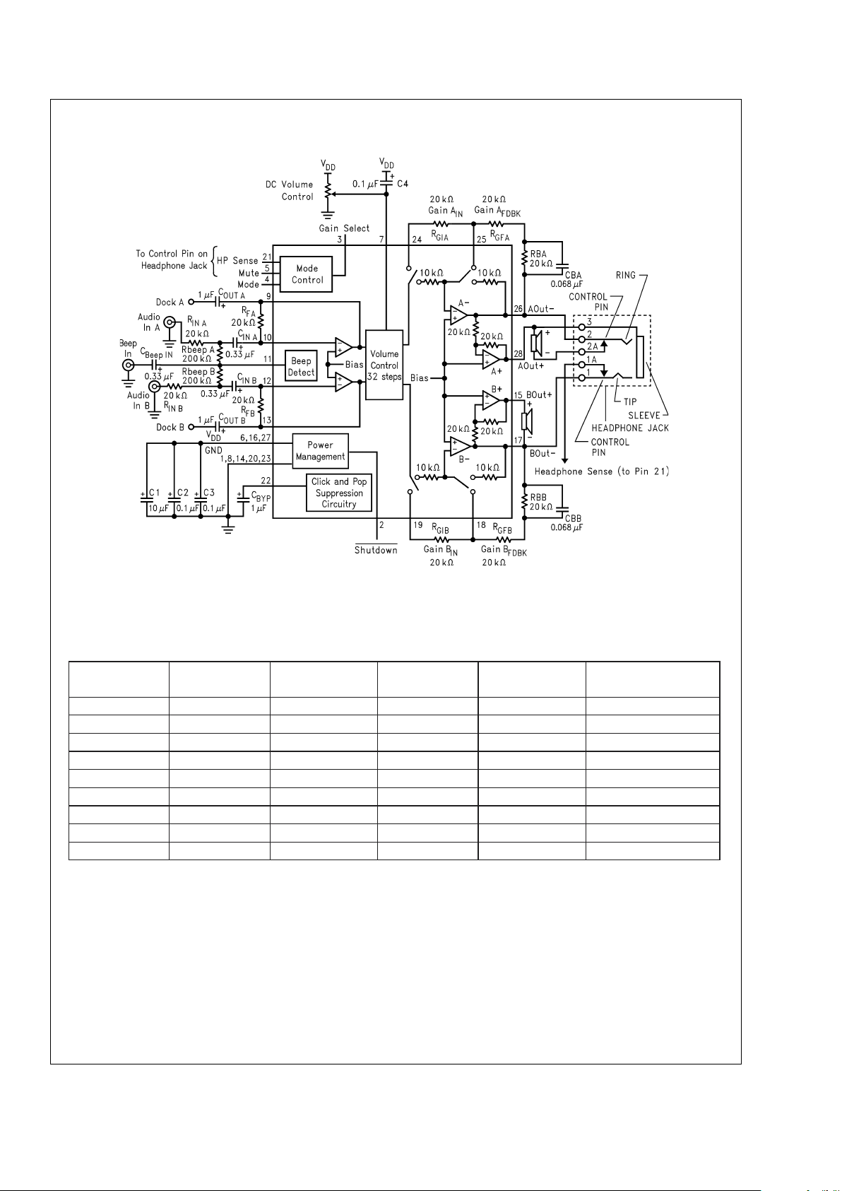
Typical Application
Truth Table for Logic Inputs
(Note 16)
Headphone
Sense
Gain Select Mode Mute Output Stage Set
To
Volume Control
X 0 0 0 Internal Gain On
X 0 0 0 Internal Gain On
X 1 0 0 External Gain On
X 1 0 0 External Gain On
On 0 1 0 Internal Gain On
Off 0 1 0 External Gain On
On 1 1 0 External Gain On
Off 1 1 0 Internal Gain On
X X X 1 X Muted
Note 16: If system beep is detected on the Beep In pin (pin 11), the system beep will be passed through the bridged amplifier regardless of the logic of the Mute
and HP sense pins.
20028003
FIGURE 2. Typical Application Circuit ( MT / MH Package Pinout )
LM4841
www.national.com5
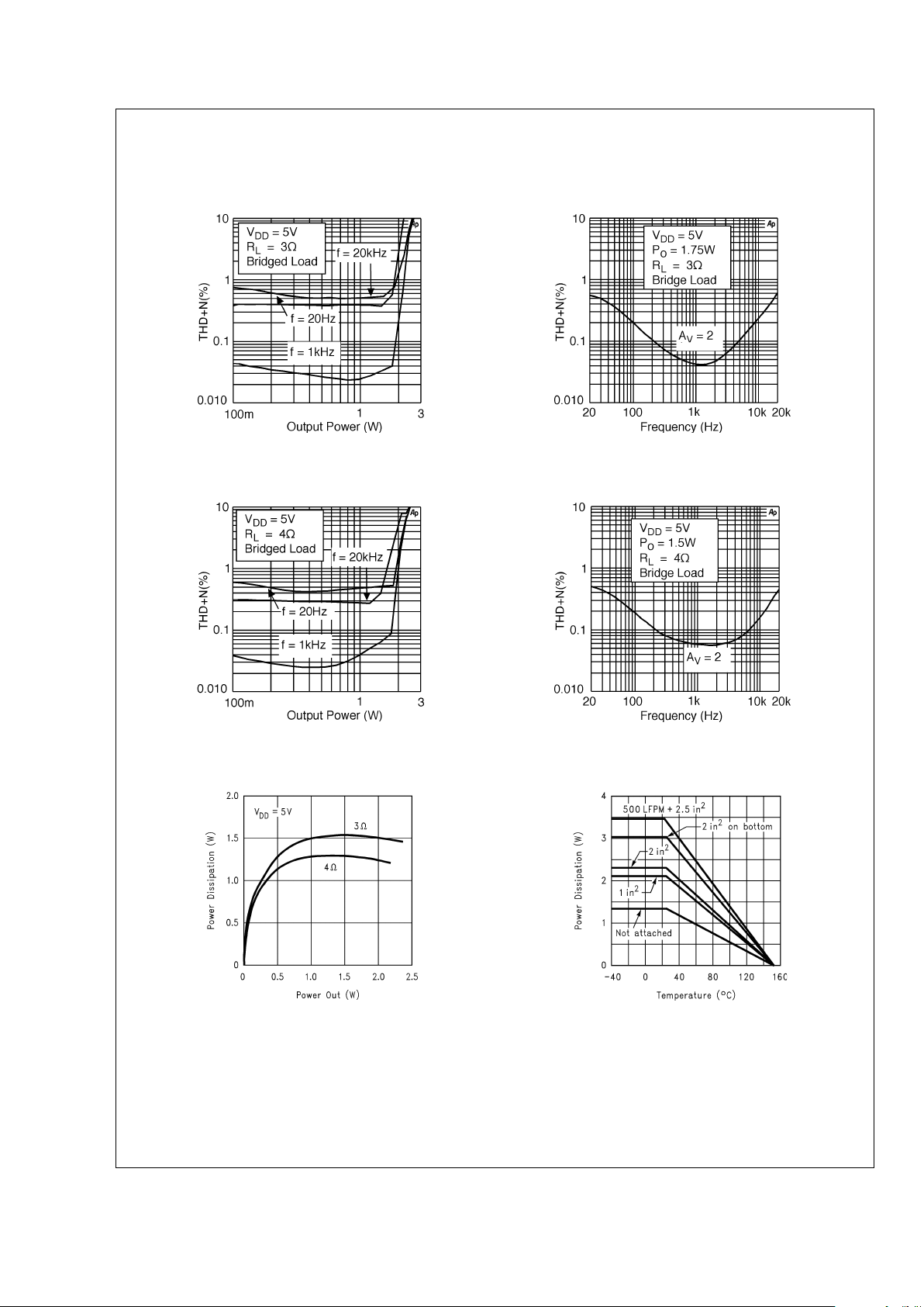
Typical Performance Characteristics
MH/LQ Specific Characteristics
LM4841MH/LQ
THD+N vs Output Power
LM4841MH/LQ
THD+N vs Frequency
20028070
20028071
LM4841MH/LQ
THD+N vs Output Power
LM4841MH/LQ
THD+N vs Frequency
20028072
20028073
LM4841MH/LQ
Power Dissipation vs Output Power
LM4841MH/LQ (Note 17)
Power Derating Curve
20028065
20028064
Note 17: These curves show the thermal dissipation ability of the LM4841MH/LQ at different ambient temperatures given these conditions:
500LFPM + 2in
2
: The part is soldered to a 2in2, 1 oz. copper plane with 500 linear feet per minute of forced-air flow across it.
2in
2
on bottom: The part is soldered to a 2in2, 1oz. copper plane that is on the bottom side of the PC board through 21 8 mil vias.
2in
2
: The part is soldered to a 2in2, 1oz. copper plane.
1in
2
: The part is soldered to a 1in2, 1oz. copper plane.
Not Attached: The part is not soldered down and is not forced-air cooled.
LM4841
www.national.com 6
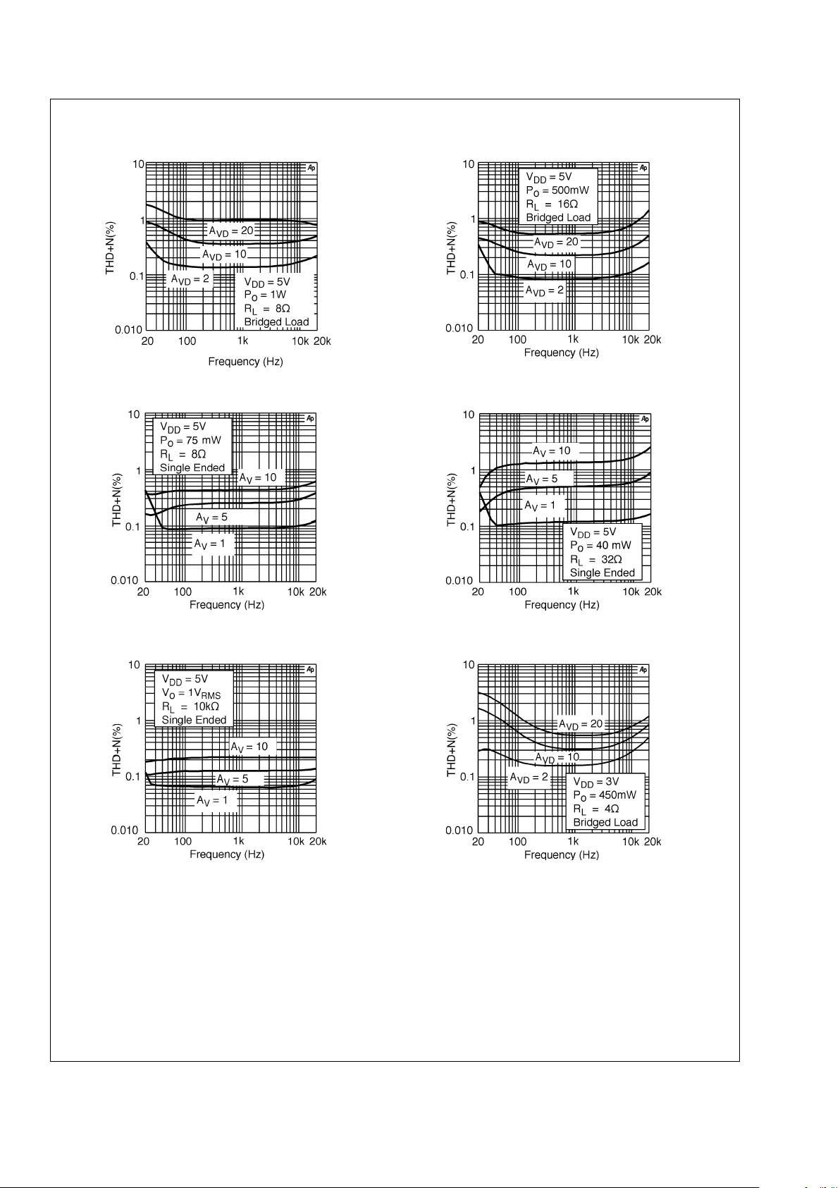
Non-MH/LQ Specific Characteristics
THD+N vs Frequency THD+N vs Frequency
20028057
20028058
THD+N vs Frequency THD+N vs Frequency
20028014
20028015
THD+N vs Frequency THD+N vs Frequency
20028016
20028017
LM4841
www.national.com7
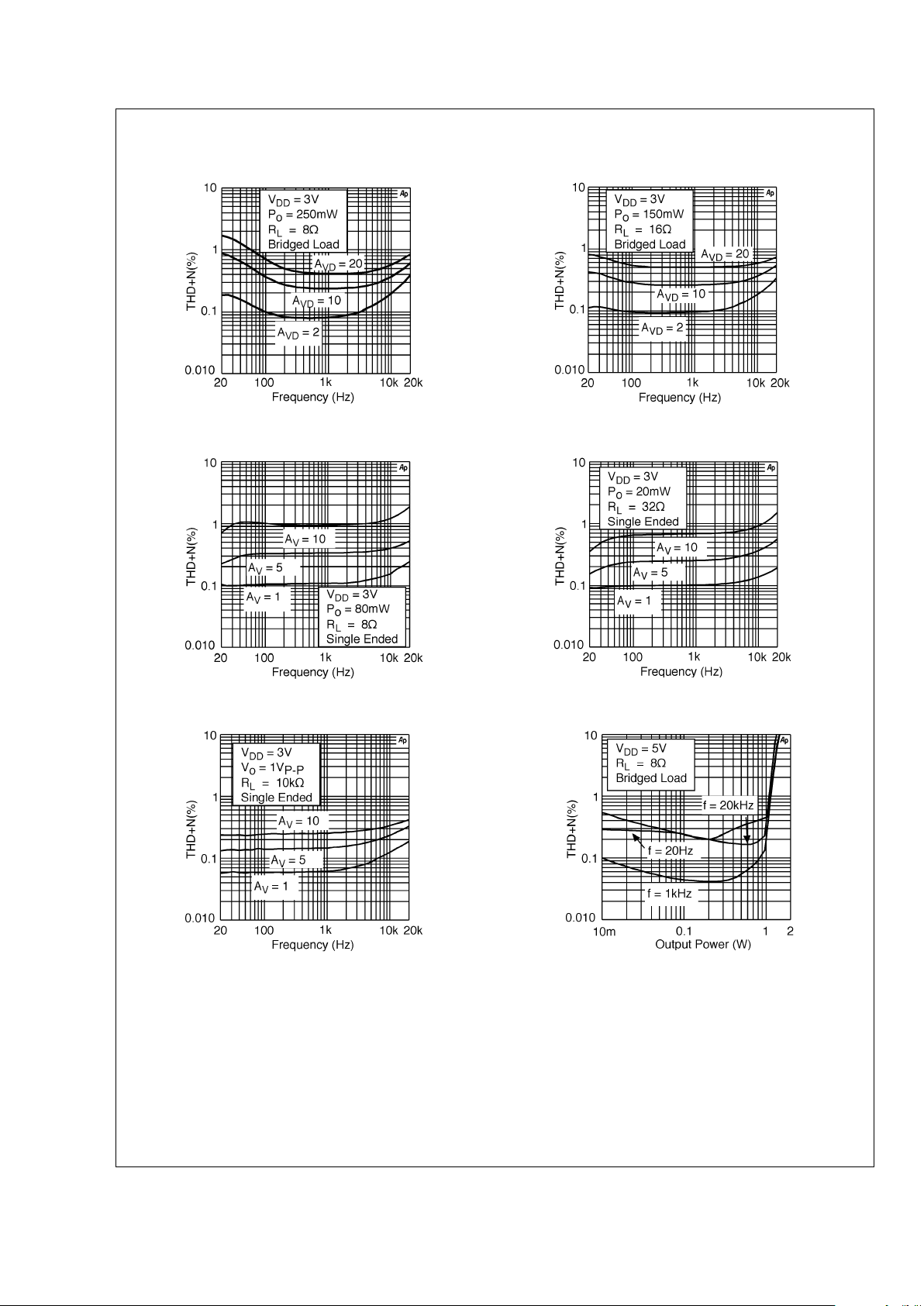
Non-MH/LQ Specific Characteristics (Continued)
THD+N vs Frequency THD+N vs Frequency
20028018 20028019
THD+N vs Frequency THD+N vs Frequency
20028020
20028021
THD+N vs Frequency THD+N vs Output Power
20028022
20028024
LM4841
www.national.com 8
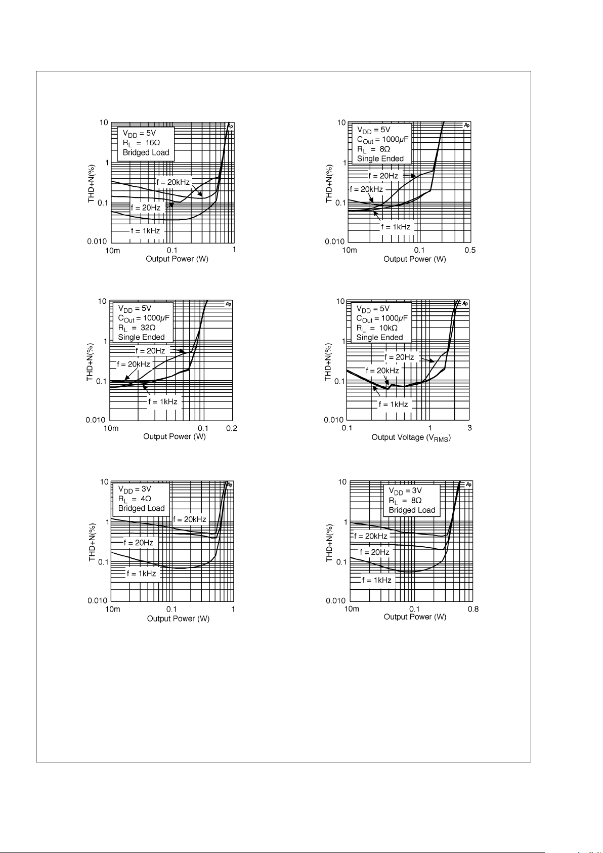
Non-MH/LQ Specific Characteristics (Continued)
THD+N vs Output Power THD+N vs Output Power
20028025
20028026
THD+N vs Output Power THD+N vs Output Power
20028027
20028028
THD+N vs Output Power THD+N vs Output Power
20028029
20028030
LM4841
www.national.com9
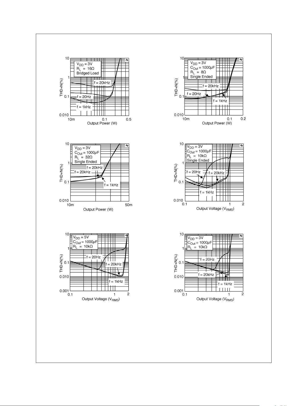
Non-MH/LQ Specific Characteristics (Continued)
THD+N vs Output Power THD+N vs Output Power
20028031
20028032
THD+N vs Output Power THD+N vs Output Power
20028033
20028034
THD+N vs Output Voltage
Docking Station Pins
THD+N vs Output Voltage
Docking Station Pins
20028059
20028060
LM4841
www.national.com 10
 Loading...