

NSC LM4838MTEX, LM4838MTE, LM4838LQX, LM4838LQ, LM4838ITL Datasheet
...
LM4838
Stereo 2W Audio Power Amplifiers
with DC Volume Control and Selectable Gain
General Description
The LM4838 is a monolithic integrated circuit that provides
DC volume control, and stereo bridged audio power amplifiers capable of producing 2W into 4Ω (Note 1) with less than
1.0% THD or 2.2W into 3Ω (Note 2) with less than 1.0%
THD.
Boomer
®
audio integrated circuits were designed specifically
to provide high quality audio while requiring a minimum
amount of external components. The LM4838 incorporates a
DC volume control, stereo bridged audio power amplifiers
and a selectable gain or bass boost, making it optimally
suited for multimedia monitors, portable radios, desktop, and
portable computer applications.
The LM4838 features an externally controlled, low-power
consumption shutdown mode, and both a power amplifier
and headphone mute for maximum system flexibility and
performance.
Note 1: When properly mounted to the circuit board, the LM4838LQ and
LM4838MTE will deliver 2W into 4Ω. The LM4838MT and LM4838ITL will
deliver 1.1W into 8Ω. See Application Information section Exposed-DAP
package PCB Mounting Considerations for more information.
Note 2: An LM4838LQ and LM4838MTE that have been properly mounted
to the circuit board and forced-air cooled will deliver 2.2W into 3Ω.
Key Specifications
n POat 1% THD+N
n into 3Ω (LQ & MTE) 2.2W (typ)
n into 4Ω (LQ & MTE) 2.0W (typ)
n into 8Ω (MT, MTE, ITL, & LQ) 1.1W (typ)
n Single-ended mode - THD+N at 85mW into
32Ω 1.0%(typ)
n Shutdown current 0.7µA (typ)
Features
n DC Volume Control Interface
n System Beep Detect
n Stereo switchable bridged/single-ended power amplifiers
n Selectable internal/external gain and bass boost
n “Click and pop” suppression circuitry
n Thermal shutdown protection circuitry
Applications
n Portable and Desktop Computers
n Multimedia Monitors
n Portable Radios, PDAs, and Portable TVs
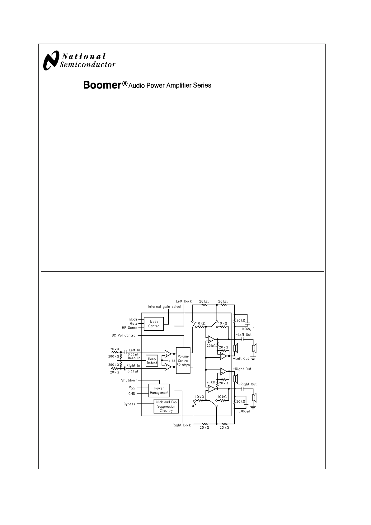
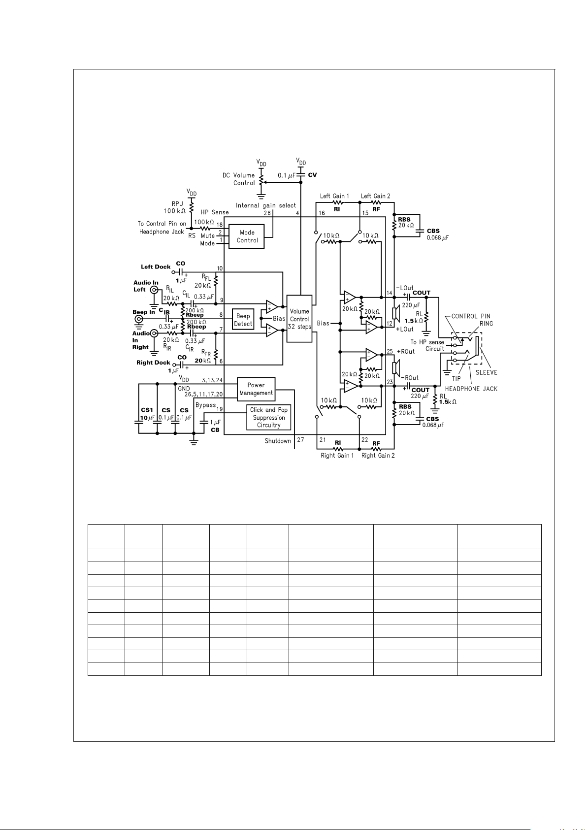
Block Diagram
Boomer®is a registered trademark of NationalSemiconductor Corporation.
20013301
FIGURE 1. LM4838 Block Diagram
January 2003
LM4838 Stereo 2W Audio Power Amplifiers with DC Volume Control and Selectable Gain
© 2003 National Semiconductor Corporation DS200133 www.national.com
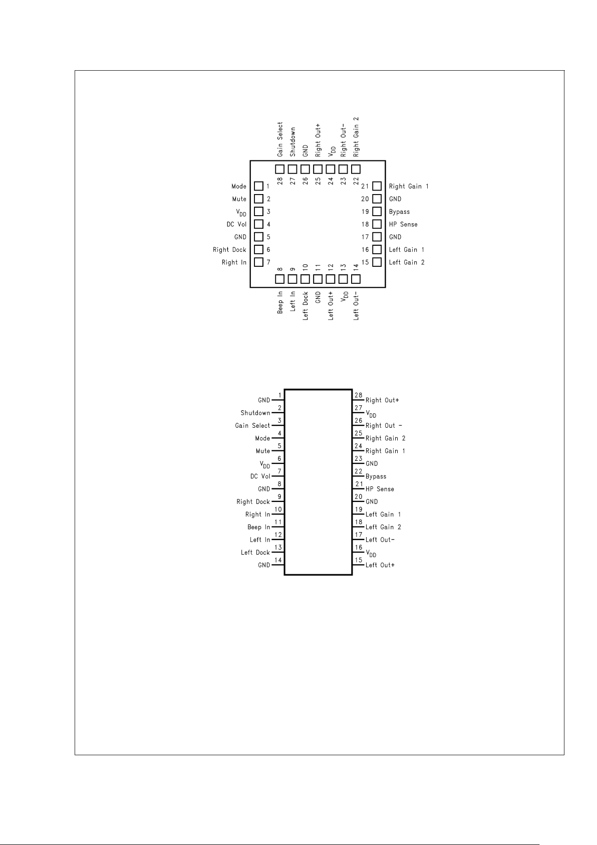
Connection Diagrams
LLP Package
20013335
Top View
Order Number LM4838LQ
See NS Package Number LQA028AA for Exposed-DAP LLP
TSSOP Package
20013302
Top View
Order Number LM4838MT
See NS Package Number MTC28 for TSSOP
Order Number LM4838MTE
See NS Package Number MXA28A for Exposed-DAP TSSOP
LM4838
www.national.com 2
Connection Diagrams (Continued)
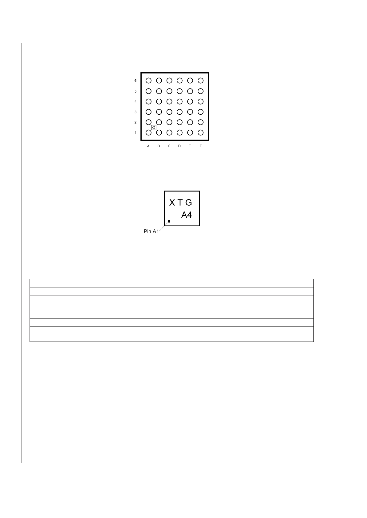
36 Bump micro SMD
20013388
Top View
Order Number LM4838ITL, LM4838ITLX
See NS Package Number TLA36AAA
micro SMD Marking
20013387
Top View
X - Date Code
T - Die Traceability
G - Boomer Family
A4 - LM4838ITL
6 NC Right Out - V
DD
Right Out + GND NC
5 GND Right Gain 2 Right Gain 1 Gain Select Shutdown Mode
4 Bypass NC NC DC Vol Mute V
DD
3 HP Sense NC NC Beep In Right Dock GND
2 GND Left Gain 2 Left Gain 1 Left In Left Dock Right In
1 NC Left Out - V
DD
Left Out + GND NC
Pin
Designator
AB C D E F
LM4838
www.national.com3
Absolute Maximum Ratings (Note 10)
If Military/Aerospace specified devices are required,
please contact the National Semiconductor Sales Office/
Distributors for availability and specifications.
Supply Voltage 6.0V
Storage Temperature -65˚C to +150˚C
Input Voltage −0.3V to V
DD
+0.3V
Power Dissipation (Note 11) Internally limited
ESD Susceptibility (Note 12) 2000V
ESD Susceptibility (Note 13) 200V
Junction Temperature 150˚C
Soldering Information
Small Outline Package
Vapor Phase (60 sec.) 215˚C
Infrared (15 sec.) 220˚C
See AN-450 “Surface Mounting and their Effects on
Product Reliability” for other methods of soldering surface
mount devices.
θ
JC
(typ) —LQA028AA 3˚C/W
θ
JA
(typ) —LQA028AA 42˚C/W
θ
JC
(typ) —MTC28 20˚C/W
θ
JA
(typ) —MTC28 80˚C/W
θ
JC
(typ) —MXA28A 2˚C/W
θ
JA
(typ) —MXA28A (exposed
DAP) (Note 4)
41˚C/W
θ
JA
(typ) —MXA28A (exposed
DAP) (Note 3)
54˚C/W
θ
JA
(typ) —MXA28A (exposed
DAP) (Note 5)
59˚C/W
θ
JA
(typ) —MXA28A (exposed
DAP) (Note 6)
93˚C/W
θJA(typ) —ITL36AAA 100˚C/W
θ
JC
(typ) —ITL36AAA (Note 16) 65˚C/W
Operating Ratings
Temperature Range
T
MIN
≤ TA≤T
MAX
−40˚C ≤TA ≤ 85˚C
Supply Voltage 2.7V≤ V
DD
≤ 5.5V
Electrical Characteristics for Entire IC (Notes 7, 10)
The following specifications apply for VDD= 5V unless otherwise noted. Limits apply for TA= 25˚C.
Symbol Parameter Conditions
LM4838
Units
(Limits)
Typical
(Note 14)
Limit
(Note 15)
V
DD
Supply Voltage 2.7 V (min)
5.5 V (max)
I
DD
Quiescent Power Supply Current VIN= 0V, IO= 0A 15 30 mA (max)
I
SD
Shutdown Current V
shutdown
=V
DD
0.7 2.0 µA (max)
V
IH
Headphone Sense High Input Voltage 4 V (min)
V
IL
Headphone Sense Low Input Voltage 0.8 V (max)
Electrical Characteristics for Volume Attenuators (Notes 7, 10)
The following specifications apply for VDD= 5V. Limits apply for TA= 25˚C.
Symbol Parameter Conditions
LM4838
Units
(Limits)
Typical
(Note 14)
Limit
(Note 15)
C
RANGE
Attenuator Range Gain with V
DCVol
= 5V, No Load
±
0.75 dB (max)
Attenuation with V
DCVol
= 0V (BM &
SE)
-75 dB (min)
A
M
Mute Attenuation V
mute
= 5V, Bridged Mode (BM) -78 dB (min)
V
mute
= 5V, Single-Ended Mode (SE) -78 dB (min)
Electrical Characteristics for Single-Ended Mode Operation (Notes 7, 10)
The following specifications apply for VDD= 5V. Limits apply for TA= 25˚C.
Symbol Parameter Conditions
LM4838
Units
(Limits)
Typical
(Note 14)
Limit
(Note 15)
P
O
Output Power THD = 1.0%; f = 1kHz; RL=32Ω 85 mW
THD=10%;f=1kHz; R
L
=32Ω 95 mW
LM4838
www.national.com 4
Electrical Characteristics for Single-Ended Mode Operation (Notes 7,
10) (Continued)
The following specifications apply for VDD= 5V. Limits apply for TA= 25˚C.
Symbol Parameter Conditions
LM4838
Units
(Limits)
Typical
(Note 14)
Limit
(Note 15)
THD+N Total Harmonic Distortion+Noise V
OUT
=1V
RMS
, f=1kHz, RL= 10kΩ,
A
VD
=1
0.065 %
PSRR Power Supply Rejection Ratio C
B
= 1.0 µF, f =120 Hz,
V
RIPPLE
= 200 mVrms
58 dB
SNR Signal to Noise Ratio P
OUT
=75 mW, RL=32Ω, A-Wtd
Filter
102 dB
X
talk
Channel Separation f=1kHz, CB= 1.0 µF 65 dB
Electrical Characteristics for Bridged Mode Operation (Notes 7, 10)
The following specifications apply for VDD= 5V, unless otherwise noted. Limits apply for TA= 25˚C.
Symbol Parameter Conditions
LM4838
Units
(Limits)
Typical
(Note 14)
Limit
(Note 15)
V
OS
Output Offset Voltage VIN= 0V, No Load 5
±
50 mV (max)
P
O
Output Power THD+N=1.0%; f=1kHz; RL=3Ω
(Note 8)
2.2 W
THD+N=1.0%; f=1kHz; RL=4Ω
(Note 9)
2W
THD = 1% (max);f = 1 kHz;
R
L
=8Ω
1.1 1.0 W (min)
THD+N = 10%;f = 1 kHz; R
L
=8Ω 1.5 W
THD+N Total Harmonic Distortion+Noise P
O
= 1W, 20 Hz<f<20 kHz,
R
L
=8Ω,AVD=2
0.3 %
P
O
= 340 mW, RL=32Ω 1.0 %
PSRR Power Supply Rejection Ratio C
B
= 1.0 µF, f = 120 Hz,
V
RIPPLE
= 200 mVrms; RL=8Ω
74 dB
SNR Signal to Noise Ratio V
DD
= 5V, P
OUT
= 1.1W, RL=8Ω,
A-Wtd Filter
93 dB
X
talk
Channel Separation f=1kHz, CB= 1.0 µF 70 dB
Note 3: The θJAgiven is for an MXA28A package whose exposed-DAP is soldered to an exposed 2in2piece of 1 ounce printed circuit board copper.
Note 4: The θ
JA
given is for an MXA28A package whose exposed-DAP is soldered to a 2in2piece of 1 ounce printed circuit board copper on a bottom side layer
through 21 8mil vias.
Note 5: The θ
JA
given is for an MXA28A package whose exposed-DAP is soldered to an exposed 1in2piece of 1 ounce printed circuit board copper.
Note 6: The θ
JA
given is for an MXA28A package whose exposed-DAP is not soldered to any copper.
Note 7: All voltages are measured with respect to the ground pins, unless otherwise specified. All specifications are tested using the typical application as shown
in Figure 1.
Note 8: When driving 3Ω loads from a 5V supply the LM4838LQ, LM4838ITL and LM4838MTE must be mounted to the circuit board and forced-air cooled.
Note 9: When driving 4Ω loads from a 5V supply the LM4838LQ, LM4838ITL and LM4838MTE must be mounted to the circuit board.
Note 10: Absolute Maximum Ratings indicate limits beyond which damage to the device may occur. Operating Ratings indicate conditions for which the device is
functional, but do not guarantee specific performance limits. Electrical Characteristics state DC and AC electrical specifications under particular test conditions which
guarantee specific performance limits. This assumes that the device is within the Operating Ratings. Specifications are not guaranteed for parameters where no limit
is given, however, the typical value is a good indication of device performance.
Note 11: The maximum power dissipation must be derated at elevated temperatures and is dictated by T
JMAX
, θJA, and the ambient temperature TA. The maximum
allowable power dissipation is P
DMAX
=(T
JMAX−TA
)/θJA. For the LM4838, T
JMAX
= 150˚C, and the typical junction-to-ambient thermal resistance for each package
can be found in the Absolute Maximum Ratings section above.
Note 12: Human body model, 100 pF discharged through a 1.5 kΩ resistor.
Note 13: Machine Model, 220 pF– 240 pF discharged through all pins.
Note 14: Typicals are measured at 25˚C and represent the parametric norm.
Note 15: Limits are guaranteed to National’s AOQL ( Average Outgoing Quality Level). Datasheet min/max specification limits are guaranteed by design, test, or
statistical analysis.
LM4838
www.national.com5
Electrical Characteristics for Bridged Mode Operation (Notes 7, 10) (Continued)
Note 16: All bumps have the same thermal resistance and contribute equally when used to lower thermal resistance. The LM4838ITL demo board (views featured
in the Application Information section) is a four layer board with two inner layers. The second inner layer is a V
DD
plane with the bottom outside layer a GND plane.
The planes measure 1,900mils x 1,750mils (48.26mm x 44.45mm) and aid in spreading heat due to power dissipation within the IC.
Typical Application
Truth Table for Logic Inputs
(Note 17)
Gain
Sel
Mode Headphone
Sense
Mute Shutdown Output Stage Set To DC Volume Output Stage
Configuration
0 0 0 0 0 Internal Gain Fixed BTL
0 0 1 0 0 Internal Gain Fixed SE
0 1 0 0 0 Internal Gain Adjustable BTL
0 1 1 0 0 Internal Gain Adjustable SE
1 0 0 0 0 External Gain Fixed BTL
1 0 1 0 0 External Gain Fixed SE
1 1 0 0 0 External Gain Adjustable BTL
1 1 1 0 0 External Gain Adjustable SE
X X X 1 0 Muted X Muted
X X X X 1 Shutdown X X
Note 17: If system beep is detected on the Beep In pin, the system beep will be passed through the bridged amplifier regardless of the logic of the Mute and HP
sense pins.
20013303
FIGURE 2. Typical Application Circuit ( LQ Package Pinout )
LM4838
www.national.com 6
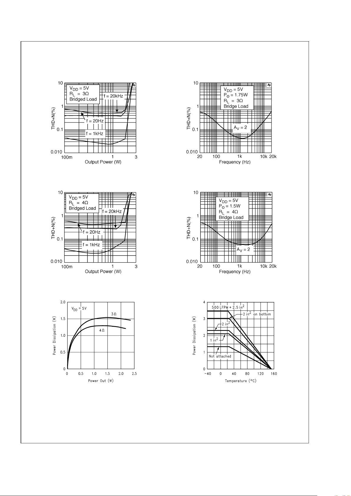
Typical Performance Characteristics
MTE Specific Characteristics
LM4838MTE
THD+N vs Output Power
LM4838MTE
THD+N vs Frequency
20013370
20013371
LM4838MTE
THD+N vs Output Power
LM4838MTE
THD+N vs Frequency
20013372
20013373
LM4838MTE
Power Dissipation vs Output Power
LM4838MTE (Note 18)
Power Derating Curve
20013365
20013364
Note 18: These curves show the thermal dissipation ability of the LM4838MTE at different ambient temperatures given these conditions:
500LFPM + 2in
2
: The part is soldered to a 2in2, 1 oz. copper plane with 500 linear feet per minute of forced-air flow across it.
2in
2
on bottom: The part is soldered to a 2in2, 1oz. copper plane that is on the bottom side of the PC board through 21 8 mil vias.
2in
2
: The part is soldered to a 2in2, 1oz. copper plane.
1in
2
: The part is soldered to a 1in2, 1oz. copper plane.
Not Attached: The part is not soldered down and is not forced-air cooled.
LM4838
www.national.com7
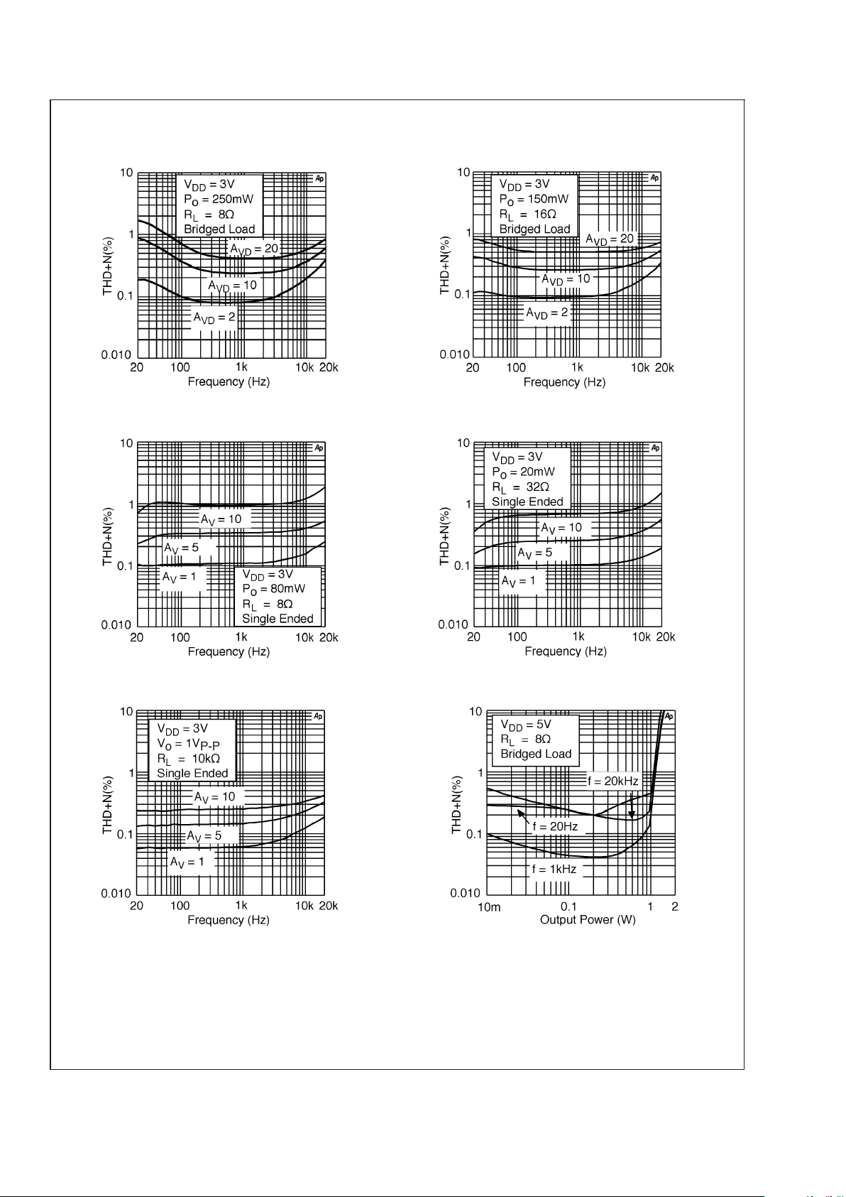
Non-MTE Specific Characteristics
THD+N vs Frequency THD+N vs Frequency
20013357
20013358
THD+N vs Frequency THD+N vs Frequency
20013314
20013315
THD+N vs Frequency THD+N vs Frequency
20013316
20013317
LM4838
www.national.com 8
Non-MTE Specific Characteristics (Continued)
THD+N vs Frequency THD+N vs Frequency
20013318 20013319
THD+N vs Frequency THD+N vs Frequency
20013320
20013321
THD+N vs Frequency THD+N vs Output Power
20013322
20013324
LM4838
www.national.com9
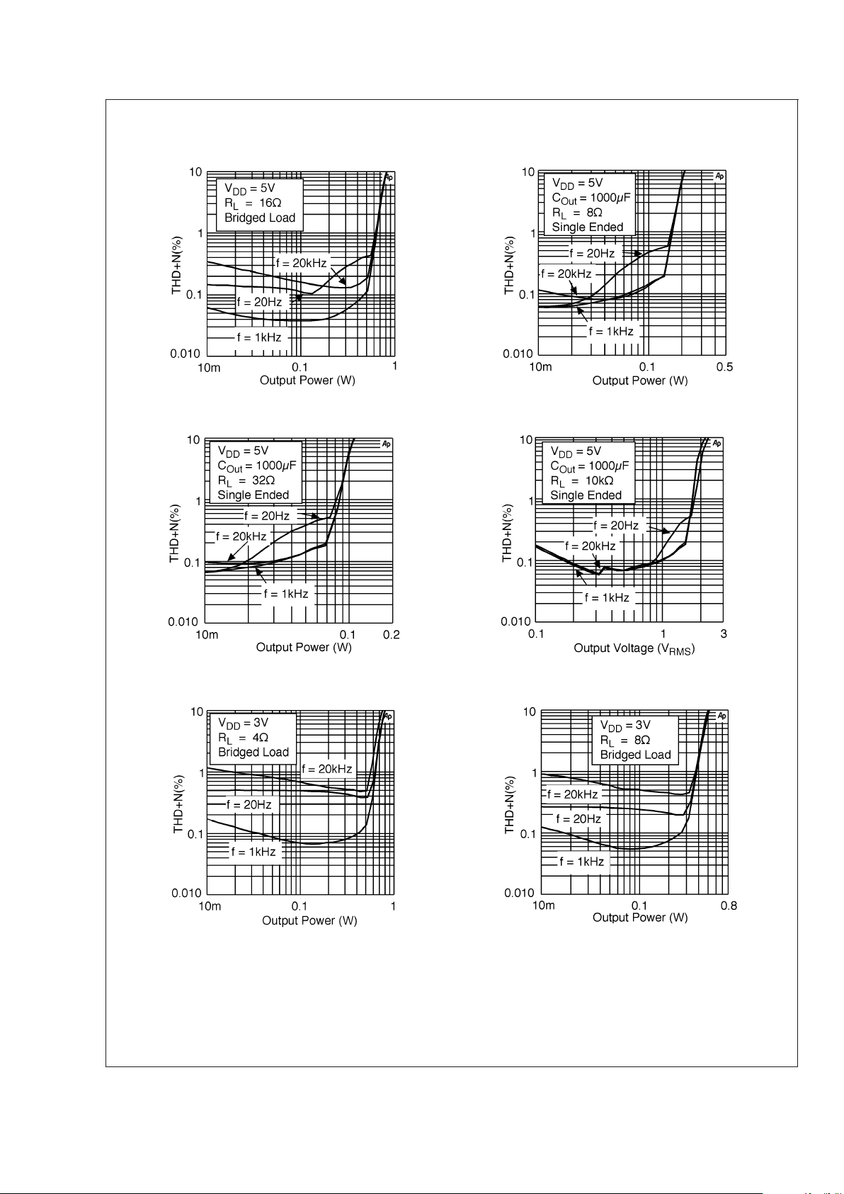
Non-MTE Specific Characteristics (Continued)
THD+N vs Output Power THD+N vs Output Power
20013325
20013326
THD+N vs Output Power THD+N vs Output Power
20013327
20013328
THD+N vs Output Power THD+N vs Output Power
20013329
20013330
LM4838
www.national.com 10
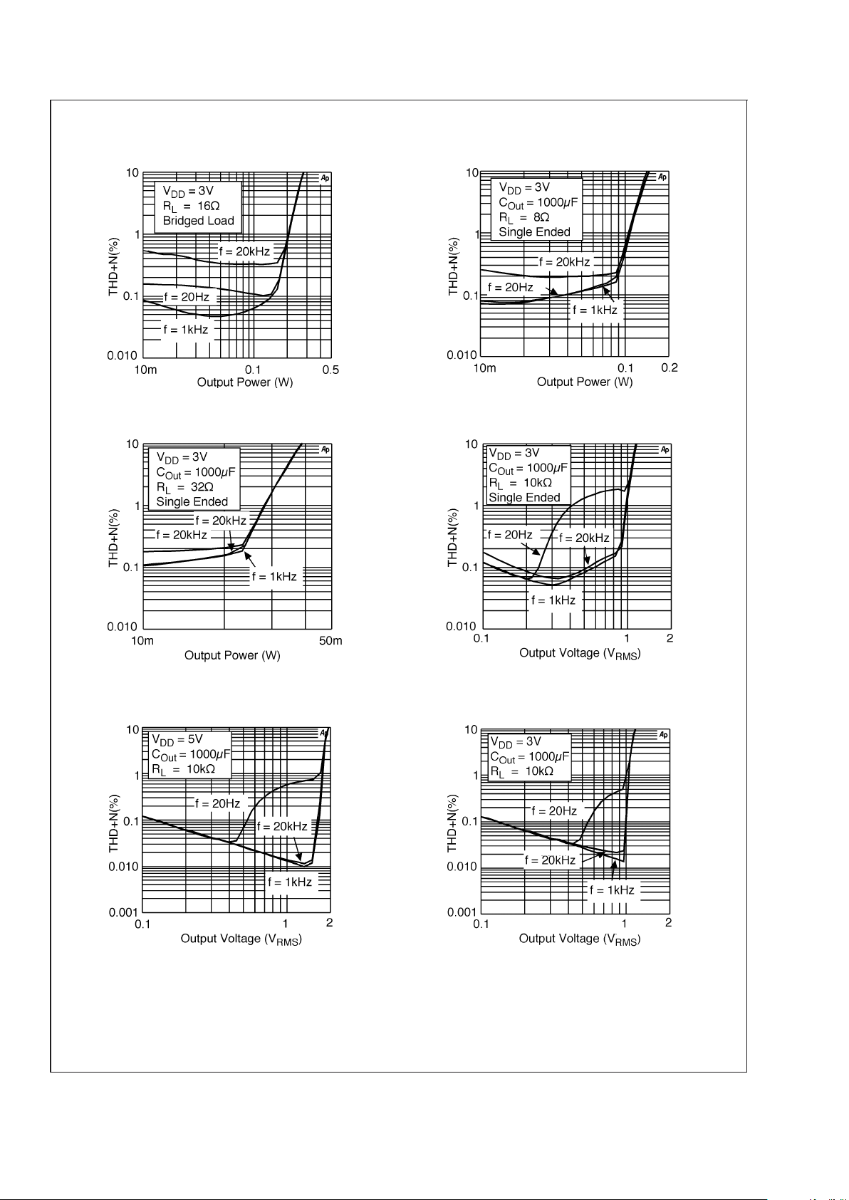
Non-MTE Specific Characteristics (Continued)
THD+N vs Output Power THD+N vs Output Power
20013331
20013332
THD+N vs Output Power THD+N vs Output Power
20013333
20013334
THD+N vs Output Voltage
Docking Station Pins
THD+N vs Output Voltage
Docking Station Pins
20013359
20013360
LM4838
www.national.com11
 Loading...