

NSC LM4832N, LM4832M, LM4832MX Datasheet
LM4832
Digitally Controlled Tone and Volume Circuit with Stereo
Audio Power Amplifier, Microphone Preamp Stage and
National 3D Sound
General Description
The LM4832 is a monolithic integrated circuit that provides
volume and tone (bass and treble) controls as well as a stereo audio power amplifier capable of producing 250 mW
(typ) into 8Ω or 90 mW (typ) into 32Ω with less than 1.0
%
THD. In addition, a two input microphone preamp stage, with
volume control, capable of drivinga1kΩload is imple-
mented on chip.
The LM4832 also features National’s 3D Sound circuitry
which can be externally adjusted via a simple RC network.
For maximum system flexibility, the LM4832 has an externally controlled, low-power consumption shutdown mode,
and an independent mute for power and microphone amplifiers .
Boomer
®
audio integrated circuits were designed specifically
to provide high quality audio while requiring few external
components. Since the LM4832 incorporates tone and volume controls, a stereo audio power amplifier and a microphone preamp stage, it is optimally suited to multimedia
monitors and desktop computer applications.
Key Specifications
n Output Power at 10%into:
8Ω
32Ω
350 mW(typ)
100 mW(typ)
n THD+Nat75mWinto
32Ω at 1 kHz 0.5%(max)
n Microphone Input Referred
Noise
7 µV(typ)
n Supply Current 13 mA(typ)
n Shutdown Current 4 µA(max)
Features
n Independent Left and Right Output Volume Controls
n Treble and Bass Control
n National 3D Sound
n I
2
C Compatible Interface
n Two Microphone Inputs with Selector
n Software Controlled Shutdown Function
Applications
n Multimedia Monitors
n Portable and Desktop Computers
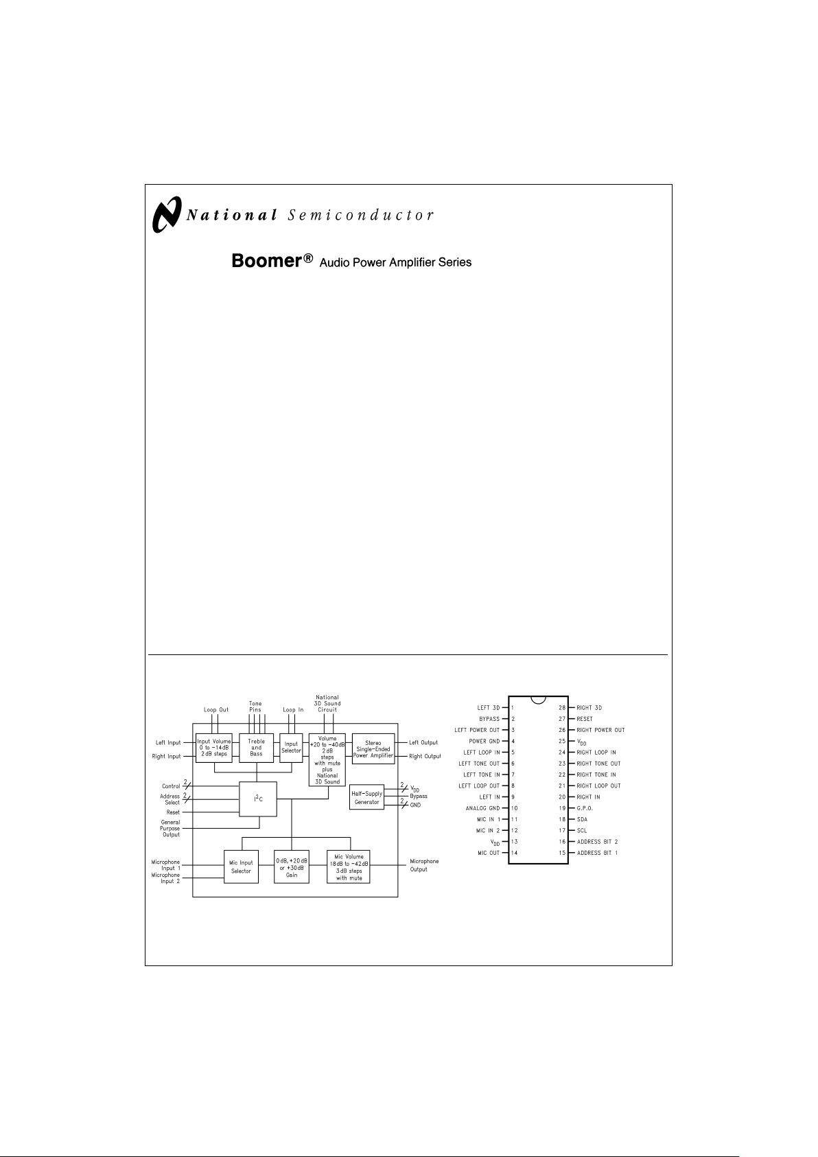
Block Diagram Connection Diagram
Boomer®is a registered trademark of National Semiconductor Corporation.
DS100014-1
FIGURE 1. LM4832 Block Diagram
DS100014-2
Top View
Order Number LM4832N, LM4832M
See NS Package Number N28B for DIP
See NS Package Number M28B for SOIC
February 1998
LM4832 Digitally Controlled Tone and Volume Circuit with Stereo Audio Power Amplifier,
Microphone Preamp Stage and National 3D Sound
© 1998 National Semiconductor Corporation DS100014 www.national.com
Absolute Maximum Ratings (Note 2)
If Military/Aerospace specified devices are required,
please contact the National SemiconductorSales Office/
Distributors for availability and specifications.
Supply Voltage 6.0V
Storage Temperature −65˚C to +150˚C
Input Voltage −0.3V to V
DD
+0.3V
Power Dissipation (Note 3) Internally limited
ESD Susceptibility (Note 4) 2000V
ESD Susceptibility (Note 5) 250V
Junction Temperature 150˚C
Soldering Information
Small Outline Package
Vapor Phase (60 sec.) 215˚C
Infrared (15 sec.) 220˚C
See AN-450 ″Surface Mounting and their Effects on
Product Reliability″ for other methods of soldering
surface mount devices.
θ
JC
(typ)—N28B 21˚C/W
θ
JA
(typ)—N28B 62˚C/W
θ
JC
(typ)—M28B 15˚C/W
θ
JA
(typ)—M28B 69˚C/W
Operating Ratings
Temperature Range
T
MIN
≤ TA≤ T
MAX
−40˚C ≤ TA≤ 85˚C
Supply Voltage 4.5 ≤ V
DD
≤ 5.5V
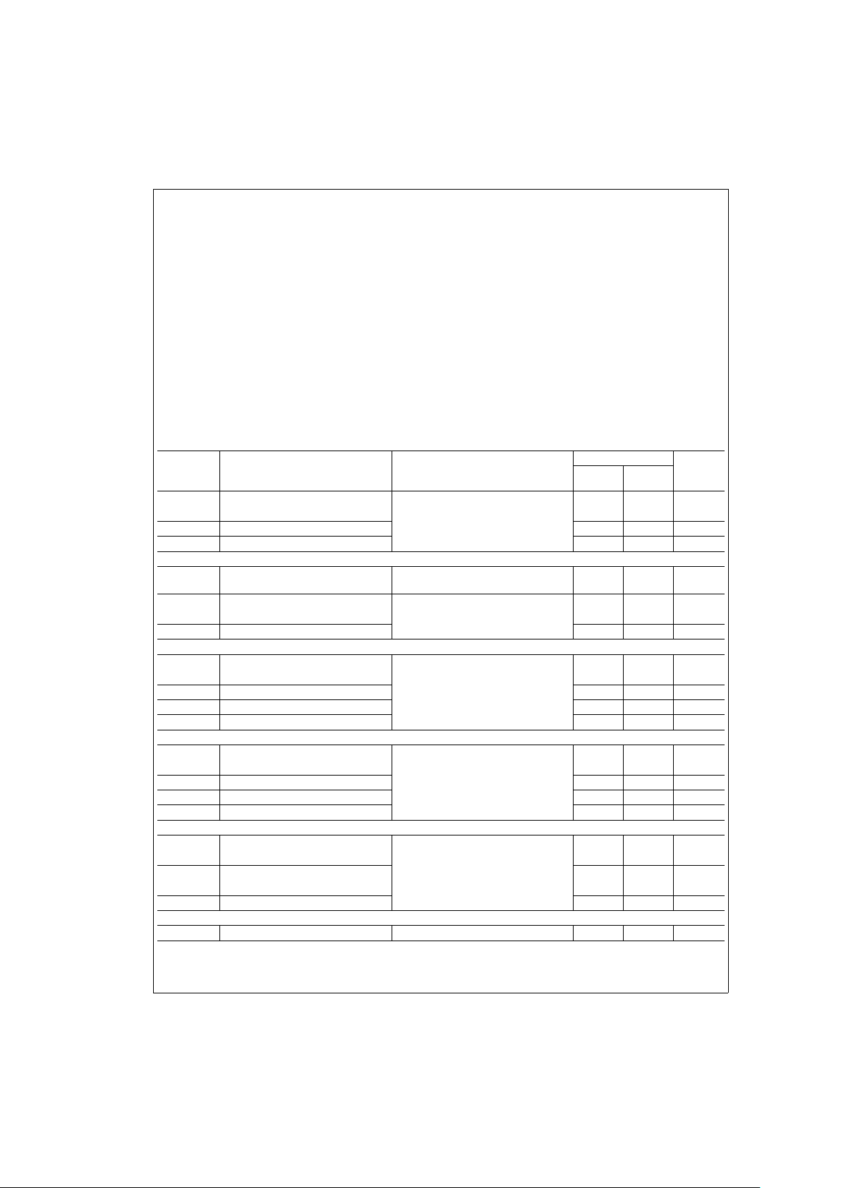
Electrical Characteristics for Entire IC(Notes 1, 2)
The following specifications apply for VDD= 5V unless otherwise noted. Limits apply for TA= 25˚C.
Symbol Parameter Conditions
LM4832
Units
(Limits)
Typical
(Note 6)
Limit
(Note 7)
V
DD
Supply Voltage VIN= 0V, IO= 0A 4.5 V (min)
5.5 V (max)
I
DD
Quiescent Power Supply Current 13 21 mA (max)
I
SD
Shutdown Current 2.5 9 µA (max)
INPUT ATTENUATORS
A
R
Attenuator Range Attenuation at 0 dB Setting
Attenuation at −14 dB Setting
1
−15
dB (max)
dB (min)
A
S
Step Size 0 dB to −14 dB 2 dB
Gain Step Size Error 0.1 dB (max)
E
T
Channel to Channel Tracking Error 0.15 dB (max)
BASS CONTROL
A
R
Bass Control Range f = 100 Hz, VIN= 0.25V
±
12 −14 dB (min)
14 dB (max)
A
S
Bass Step Size 2 dB
E
SE
Bass Step Size Error 0.5 dB (max)
E
T
Bass Tracking Error 0.15 dB (max)
TREBLE CONTROL
A
R
Treble Control Range fIN= 10 kHz, VIN= 0.25V
±
12 −13 dB (min)
13 dB (max)
A
S
Treble Step Size 2 dB
E
SE
Treble Step Size Error 0.1 dB (max)
E
T
Treble Tracking Error 0.15 dB (max)
OUTPUT ATTENUATORS
A
R
Attenuator Range Gain at +20 dB Setting
Attenuation at −40 dB Setting
+20 dB to −40 dB
21 dB (max)
−42 dB (min)
A
S
Step Size 2dB
Step Size Error 0.1 dB (max)
E
T
Channel to Channel Tracking Error 0.1 dB (max)
AUDIO PATH
V
OS
Output Offset Voltage VIN= 0V 3 50 mV (max)
www.national.com 2
Electrical Characteristics for Entire IC(Notes 1, 2) (Continued)
The following specifications apply for VDD= 5V unless otherwise noted. Limits apply for TA= 25˚C.
Symbol Parameter Conditions
LM4832
Units
(Limits)
Typical
(Note 6)
Limit
(Note 7)
AUDIO PATH
P
O
Output Power THD = 1.0%(max),f=1kHz, All
controls at 0dB
R
L
=8Ω 250 mW (min)
R
L
=32Ω 95 75 mW (min)
THD+N Total Harmonic Distortion+Noise All Controls at 0 dB, THD = 10%,f=1
kHz
R
L
=8Ω 350 mW
P
O
= 200 mW, RL=8Ω 0.15
%
P
O
= 75 mW, RL=32Ω 0.11
%
V
O
= 1 Vrms, RL=10Ω 0.08
%
PSRR Power Supply Rejection Ratio C
B
= 1 µF, f = 100 Hz, V
RIPPLE
= 100
mVrms, All Controls at 0 dB Setting
45 dB
A
M
Mute Attenuation f = 1 kHz, VIN= 1V −75 dB
X
TALK
Cross Talk PO= 200 mW, RL=8Ω,
All controls at 0 dB setting,
f=1kHz
Left to Right −85 dB
Right to Left −72 dB
MICROPHONE PREAMP AND VOLUME CONTROL
A
V
Preamp Gain 0 dB Gain 0 −1, 1 dB
+20 dB Gain 20 19, 21 dB
+30 dB Gain 30 29, 31 dB
A
R
Attenuator Range Gain at +18 dB Setting 20 dB (max)
Attenuation at −42 dB Setting −43 dB (min)
A
S
Step Size 0 dB to −42 dB 3 dB
Step Size Error 0.4 dB (max)
V
SWING
Output Voltage Swing f = 1 kHz, THD<1.0%,RL=1kΩ 1.7 V
rms
E
NO
Input Referred Noise A-Weighted, Attenuator at 0 dB 7 µV (min)
PSRR Power Supply Rejection Ratio f = 100 Hz, V
RIPPLE
= 100 mVrms,
C
B
=1µF
35 dB
A
M
Mute Attenuation −90 dB
X
TALK
Cross Talk Power Amp PO=200mW,f=1kHz −90 dB
THD+N Total Harmonic Distortion Plus Noise All controls at 0 dB,f=1kHz, V
O
=1V
0 dB Setting 0.03
%
+20 dB Gain 0.03
%
+30 dB Gain 0.04
%
I
2
C BUS TIMING
f
MAX
Maximum Bus Frequency 400 kHz
T
START:HOLD
Start Signal: Hold Time before
Clock/Data Transitions
0.6 µs
T
D;SETUP
Data Setup Time 0.1 µs
T
C;HIGH
Minimum High Clock Duration 0.6 µs
T
C;LOW
Minimum Low Clock Duration 1.3 µs
T
STOP;SETUP
Stop Signal: Setup Time before
Clock/Data Transitions
0.6 µs
I
2
C BUS INPUT AND OUTPUT
V
IL
Input Low Voltage 1.5 V (max)
3 www.national.com
Electrical Characteristics for Entire IC(Notes 1, 2) (Continued)
The following specifications apply for VDD= 5V unless otherwise noted. Limits apply for TA= 25˚C.
Symbol Parameter Conditions
LM4832
Units
(Limits)
Typical
(Note 6)
Limit
(Note 7)
I
2
C BUS INPUT AND OUTPUT
V
IH
Input High Voltage 3 V (min)
I
IN
Input Current 0.15 µA
V
O
Output Voltage—SDA Acknowledge 0.4 V (max)
V
OL
External Power Amp Disable Low 0.4 V (max)
V
OH
External Power Amp Disable High 4 V (min)
Note 1: All voltages are measured with respect to the ground pins, unless otherwise specified. All specifications are tested using the typical applicationas shown in
Figure 1
.
Note 2: Absolute Maximum Ratings indicatelimitsbeyondwhich damage to the device may occur. Operating Ratings indicate conditions for which the device is functional, but do not guarantee specific performance limits. Electrical Characteristics state DC and AC electrical specifications under particular test conditions which guarantee specific performance limits. This assumes that the device is within the Operating Ratings. Specifications are not guaranteed for parameters where no limit is
given, however, the typical value is a good indication of device performance.
Note 3: The maximum power dissipation must be derated at elevated temperatures and is dictated by T
JMAX
, θJA, and the ambient temperature TA. The maximum
allowable power dissipation is P
DMAX
=(T
JMAX−TA
)/θJA.For the LM4832, T
JMAX
= 150˚C, and the typical junction-to-ambient thermal resistance, when board
mounted, is 69˚C/W assuming the M28B package.
Note 4: Human body model, 100 pF discharged through a 1.5 kΩ resistor.
Note 5: Machine Model, 220 pF–240 pF discharged through all pins.
Note 6: Typicals are measured at 25˚C and represent the parametric norm.
Note 7: Limits are guaranteed that all parts are tested in production to meet the stated values.
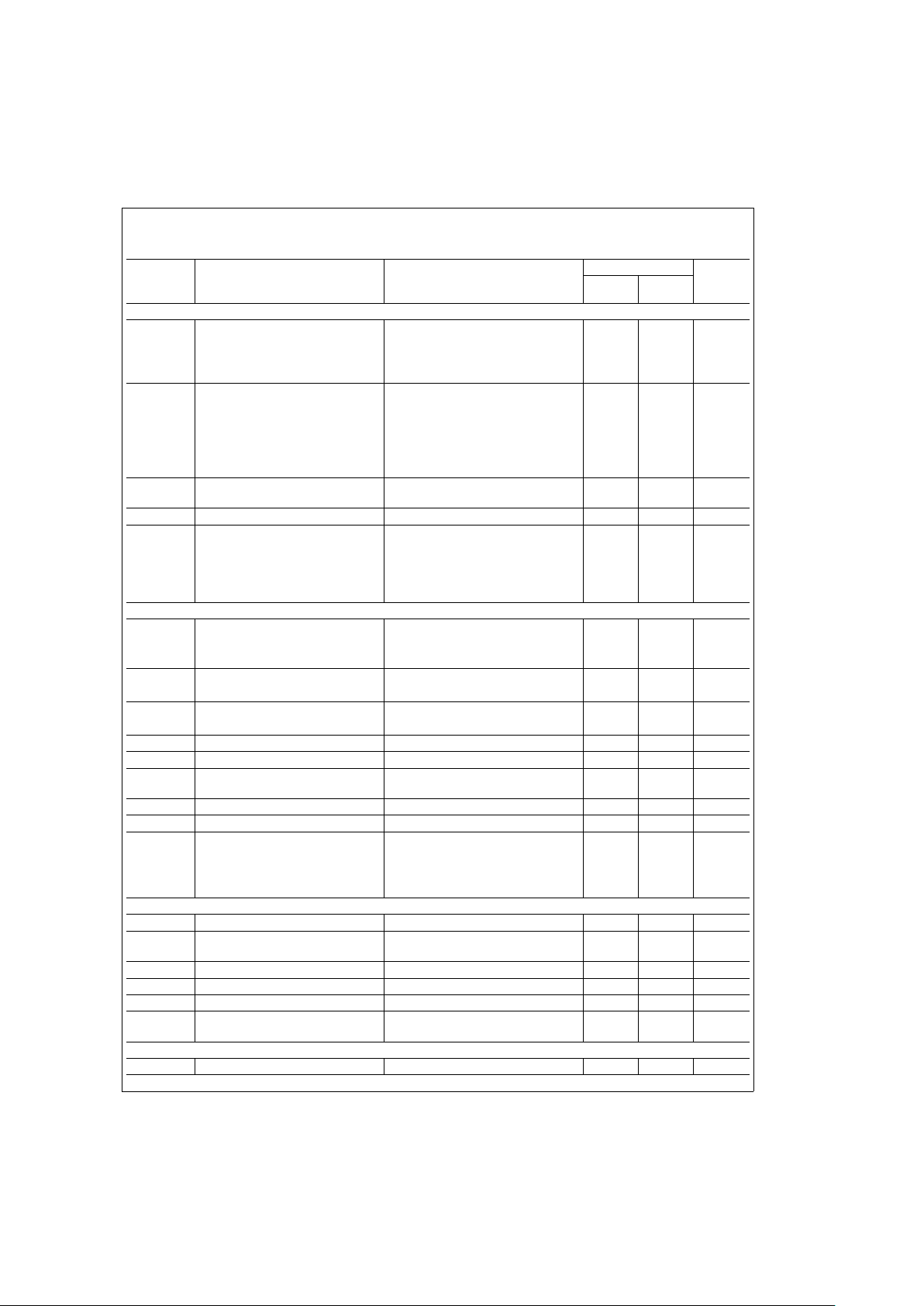
Typical Application Circuit
DS100014-3
FIGURE 2. Typical Application Circuit
www.national.com 4

Pin Description
LEFT 3D (1)
RIGHT 3D
(28)
An external RC network is connected
across these pins. This function provides
left-right channel cross coupling and
cancellation to create an enhanced
stereo channel separation effect.
BYPASS (2) A 0.1 µF capacitor is placed between
this pin and ground to provide an AC
ground for the internal half-supply
voltage reference. The capacitor at this
pin affects “click-pop” and THD
performance. Turn-on and turn-off times
are also determined by this capacitor.
Refer to the Application Information
section for more information.
POWER
AMP OUT
LEFT (3)
RIGHT (26)
These outputs are intended to drive 8Ω
speakers or 32Ω headphones. These
outputs should be AC-coupled to the
loads. Refer to the Application
Information section for more information.
POWER
GND (4)
This pin provides the high current return
for the power output stage MOSFETs
and digital circuitry.
LOOP OUT
(8, 21)
LOOP IN (5,
24)
These pins allow an external signal
processor access to the stereo signal.
Please see the Application Information
section for more information.
TONE OUT
(6, 23)
These pins are connected to the tone
control op amp outputs and drive the
power amplifier inputs. Refer to the
Application Information section for more
information.
TONE IN
(7, 22)
These pins are connected to the inputs
of the tone control op amps. A capacitor
between the Tone In and Tone Out pins
sets the frequency response of the tone
functions. Please refer to the Application
Information section for more information.
INPUTS
(9, 20)
These pins are the stereo inputs for the
LM4832. These pins should be
AC-coupled to the input signals.
ANALOG
GND (10)
This pin is the AC analog ground for the
line level AC signal inputs.
MIC
INPUTS
(11, 12)
These pins are the two independent
selectable microphone inputs. These
pins should be AC-coupled.
MIC OUT
(14)
This pin is the output for the microphone
amplifier and should be AC-coupled to
the load.
V
DD
(13, 25)
These pins are for the 5V supply. These
pins should be separately bypassed by
0.1 µF, or higher, film capacitors. The 5V
supply should be bypassed by a 10 µF,
or higher, tantalum or aluminum
electrolytic capacitor.
ADDRESS
BITS (15,
16)
These pins are used to determine the
I
2
C address for the LM4832.
CLOCK (17) This pin is the input for the I
2
C clock
signal.
DATA (18) This pin is the input for the I
2
C data
signal.
GENERAL
PURPOSE
OUTPUT
(19)
This pin provides a general purpose
TTL/CMOS output. Please refer to the
Application Information section for more
information.
RESET (27) This pin is a TTL/CMOS input which is
used to reset the chip logic and states.
5 www.national.com
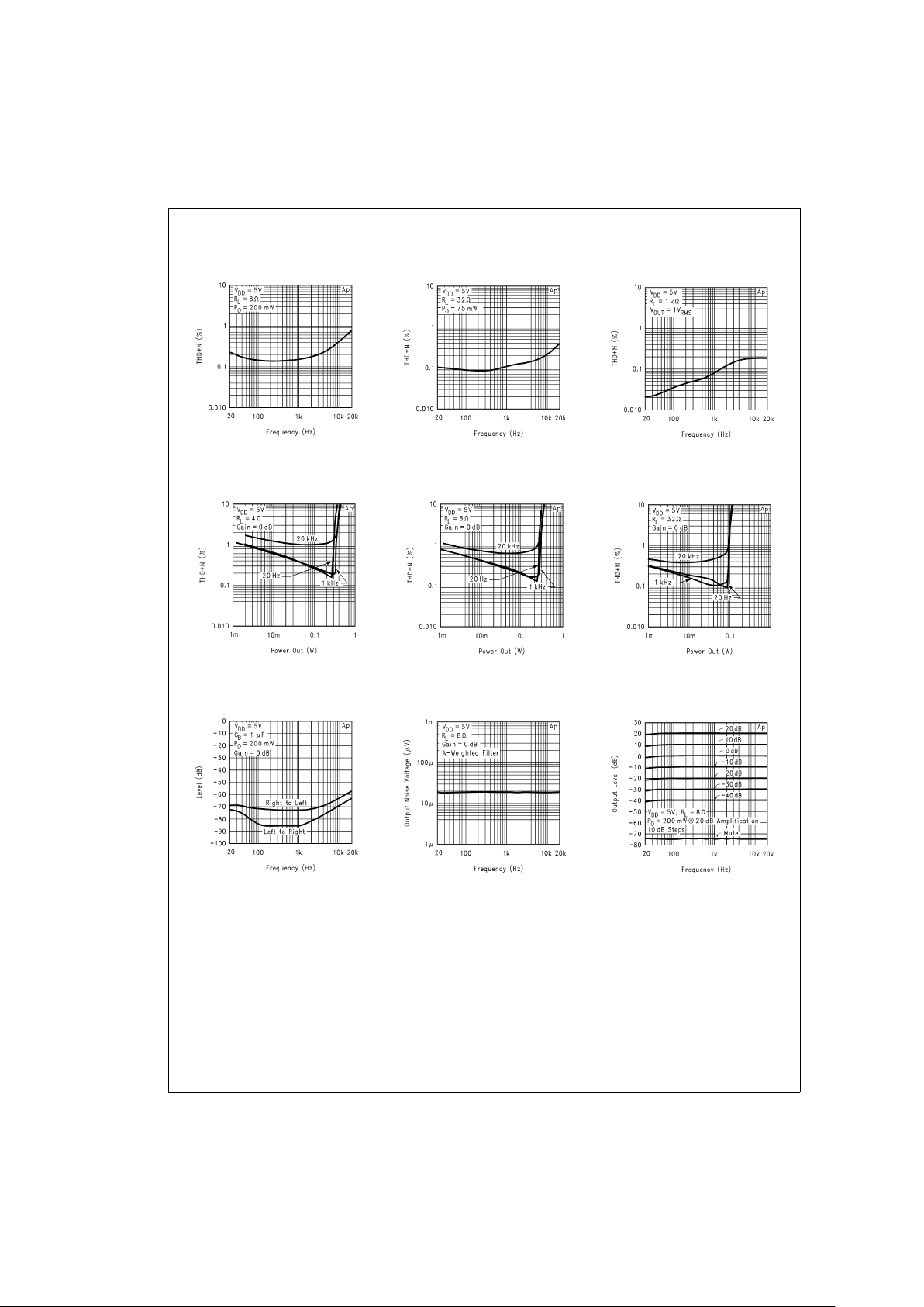
Typical Performance Characteristics
THD+N vs
Frequency, 8Ω
DS100014-4
THD+N vs
Frequency, 32Ω
DS100014-5
THD+N vs
Frequency, 1 kΩ
DS100014-6
THD+N vs
Output Power
DS100014-7
THD+N vs
Output Power
DS100014-8
THD+N vs
Output Power
DS100014-9
Power Amplifier
Crosstalk
DS100014-10
Power Amplifier
Noise Floor
DS100014-11
Power Amplifier Attenuation
vs Frequency
DS100014-12
www.national.com 6
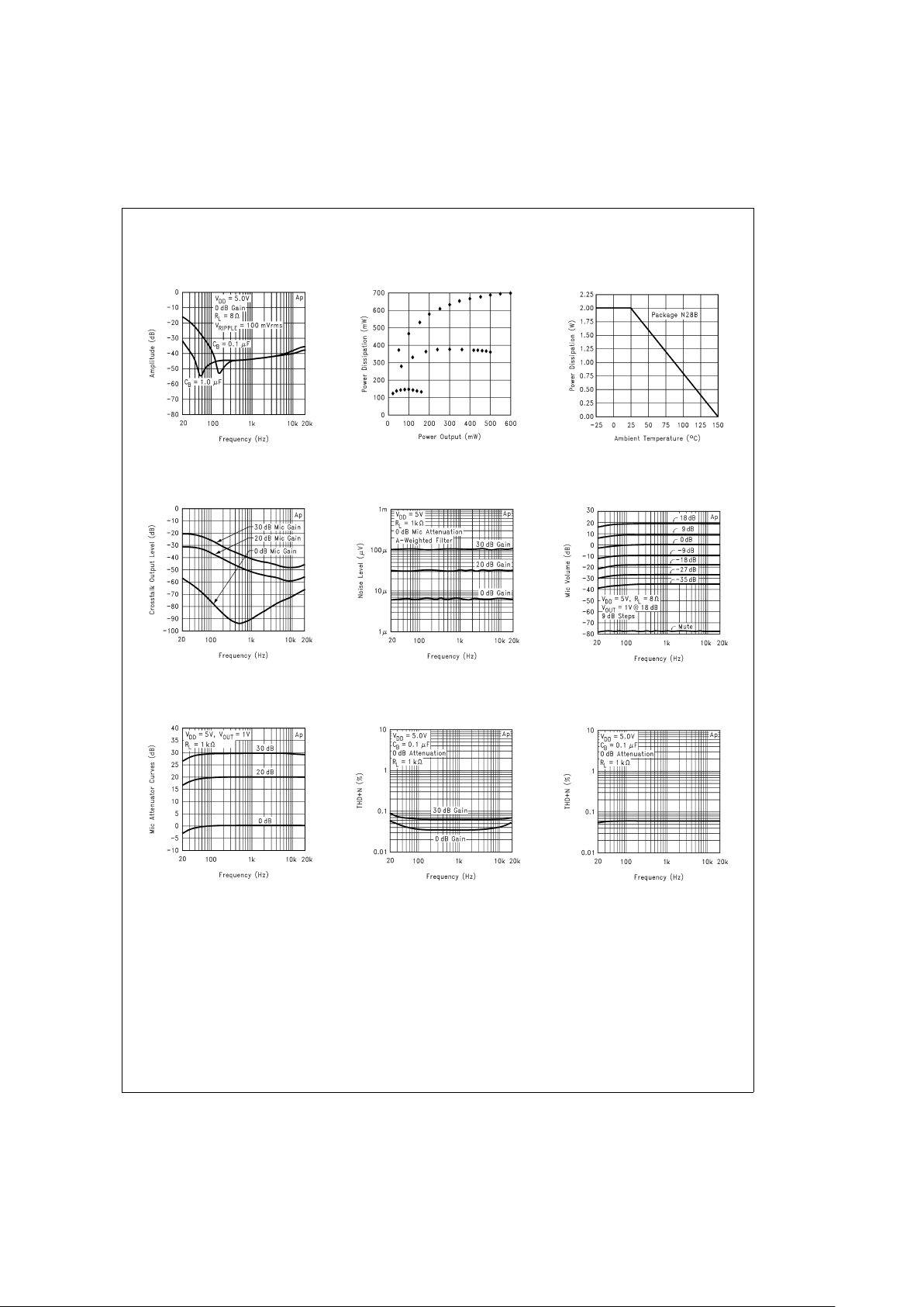
Typical Performance Characteristics (Continued)
Power Supply
Rejection Ratio
DS100014-13
Power Dissipation
vs Output Power
DS100014-14
Power Derating
Curve
DS100014-15
Mic Amplifer Crosstalk
from Power Amplifier
DS100014-16
Mic Amplifier
Noise Floor
DS100014-17
Mic Amplifier Attenuation
vs Frequency
DS100014-18
Mic Amplifier Gain
vs Frequency
DS100014-19
Mic Amplifier THD+N
vs Frequency
DS100014-20
Loop-out THD+N
vs Frequency
DS100014-21
7 www.national.com
 Loading...