

NSC LM4830MX, LM4830M, LM4830N Datasheet
LM4830
Two-Way Audio Amplification System
with Volume Control
General Description
The LM4830 is an integrated solution for two-way audio amplification. Itcontainsa bridge-connected audio power amplifier capable of delivering 1W of continuous average power to
an 8Ω load with less than 1%THD from a 5V power supply.
It also has the capability of driving 100 mW into a
single-ended 32Ω impedance for headset operation. There
is a 30 dB attenuator in front of a bridged power amplifier
with 6 dB of gain. The attenuation is controlled through 4 bits
of parallel digital control; 15 steps of 2 dB each.
The device also contains a microphone preamp with two selectable inputs. Mic2 is selected when HS is high andA1 is in
single-ended mode. Mic1 is selected when HS is low and A1
is in bridged mode. This configuration is optimum for switching between an internal system speaker and external headset with microphone. The device also incorporates a buffer
used for driving capacitive loads.
The LM4830 also provides a low-current consumption shutdown mode making it optimally suited for low-power portable
systems. In addition, the device has an internal thermal shutdown protection mechanism.
Key Specifications
n THD at 1W cont. avg POinto 8Ω:1%(max)
n Instantaneous peak output power: 1.4W
n Shutdown current: 0.5 µA (typ)
n Supply voltage range: 2.7V ≤ V
DD
≤ 5.5V
Features
n 4-bit digital control for 30 dB of volume attenuation
n Two selectable microphone inputs
n High performance microphone preamp
n Extra buffer for driving long cables
n No bootstrap capacitors or snubber circuits are
necessary
n Small Outline (SO) packaging
n Thermal shutdown protection circuitry
Applications
n Hands-free phone systems
n Mobile phone accessories
n Desktop conference phones
n Portable computers
n Teleconference computer applications
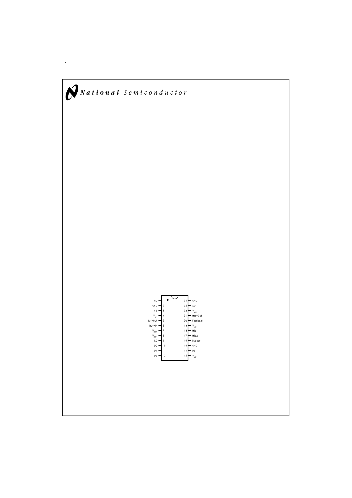
Connection Diagram
Dual-In-Line and
Small Outline Packages
DS012677-2
Top View
Order Number LM4830M
See NS Package Number M24B for SO
Order Number LM4830N
See NS Package Number N24A for DIP
January 1999
LM4830 Two-Way Audio Amplification System with Volume Control
© 1999 National Semiconductor Corporation DS012677 www.national.com
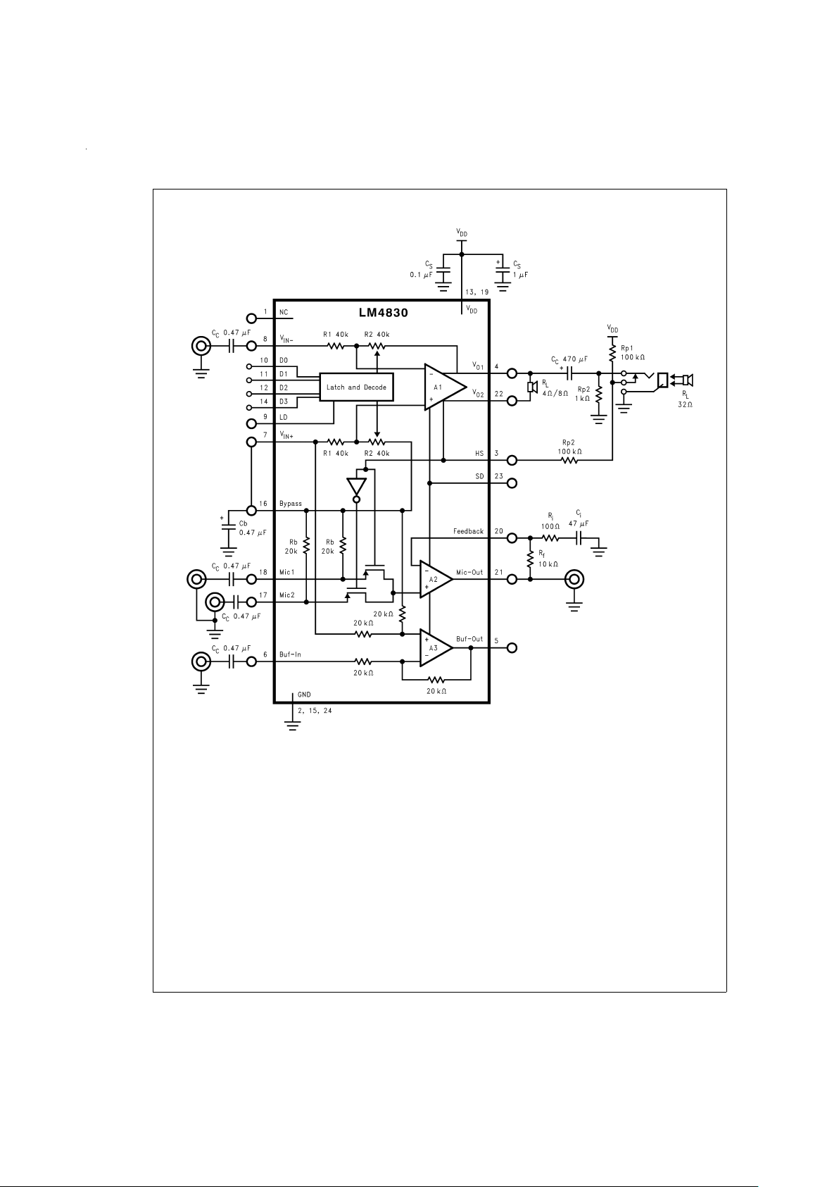
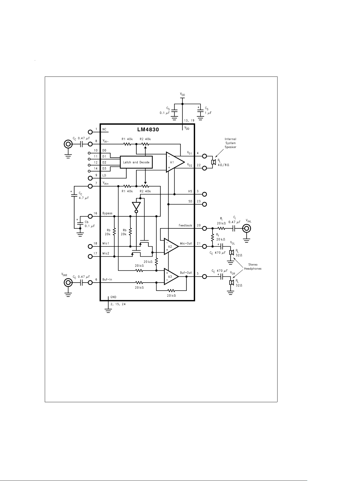
Typical Application
DS012677-1
FIGURE 1. Typical Application Circuit
www.national.com 2
Absolute Maximum Ratings (Note 2)
If Military/Aerospace specified devices are required,
please contact the National Semiconductor Sales Office/
Distributors for availability and specifications.
Supply Voltage 6.0V
Storage Temperature −65˚C to +150˚C
Input Voltage −0.3V to V
DD
+ 0.3V
Power Dissipation (Note 3) Internally Limited
ESD Susceptibility (Note 4) 2000V
ESD Susceptibility (Note 5) 250V
Junction Temperature 150˚C
Soldering Information
Small Outline Package
Vapor Phase (60 sec.) 215˚C
Infrared (15 sec.) 220˚C
See AN-450
“Surface Mounting and their Effects on
Product Reliability”
for other methods of soldering surface
mount devices.
Operating Ratings
Temperature Range
T
MIN
≤ TA≤ T
MAX
−40˚C ≤ TA≤ 85˚C
Supply Voltage 2.7V ≤ V
DD
≤ 5.5V
θ
JC
(typ)—M24B 32˚C/W
θ
JA
(typ)—M24B 79˚C/W
θ
JC
(typ)—N24A 21˚C/W
θ
JA
(typ)—N24A 61˚C/W
Electrical Characteristics (Notes 1, 2)
The following specifications apply for V
DD
=
5V, unless otherwise specified. Limits apply for T
A
=
25˚C.
Symbol Parameter Conditions LM4830 Units
(Limits)
Typical Limit
(Note 6) (Note 7)
POWER AMPLIFIER, A1
I
DD
Quiescent Power Supply Current V
O
=
0V, I
O
=
0A, R
L
=
∞
5.8 mA (min)
11.0 20.0 mA (max)
Bridged R
L
=
8Ω 11.4 mA
HS=5V, SD=0V, V
O1
On Only 7.9 mA
I
SD
Shutdown Current HS=5V, SD=5V, IC Off 0.5 2.0 µA (max)
V
OS
Output Offset Voltage V
IN
=
0V 0.7 50.0 mV (max)
e
IN
Input Noise IHF-A Weighting Filter, R
S
=
25Ω
Bridged Output, V
O1–VO2,RL
=
8Ω 30 µV
Single-Ended Output, V
O1,RL
=
32Ω 16 µV
P
O
Output Power, Bridged THD=1%(max); f=1 kHz, R
L
=
8Ω 1.15 1.0 W (min)
THD+N=10%;f=1 kHz, R
L
=
8Ω 1.4 W
THD+N=10%;f=1 kHz, R
L
=
4Ω 2W
THD Total Harmonic Distortion f=1 kHz, Attenuation
@
0dB
P
O
=
1.5W, R
L
=
4Ω 0.2
%
P
O
=
1W, R
L
=
8Ω 0.2
%
V
O1
On Only, V
O
=
60 mV, R
L
=
32Ω 0.06
%
Attenuation Step Size Error 0 dB to −30 dB
±
0.5 dB
Absolute Attenuation Attenuation
@
0dB
±
0.5 dB
Attenuation
@
−30 dB
±
1.0 dB
R
IN
Power Amp Input Resistance 40 kΩ
DIGITAL INPUTS
V
IH
High Input Voltage CMOS Compatible Only 4.5 V
V
IL
Low Input Voltage CMOS Compatible Only 0.5 V
PREAMP, A2
R
IN
Mic1 and Mic2 Input Resistance 21.5 kΩ
V
OS
Output Offset Voltage V
IN
=
0V 2.0 mV
e
IN
Input Noise IHF-A Weighting Filter, R
S
=
25Ω 1.3 10.0 µV (max)
THD Total Harmonic Distortion A
VCL
=
100, V
IN
=
10 mVrms, f=1 kHz 0.06
%
A
VCL
=
−1, P
O
=
50 mW, f=1 kHz, R
L
=
32Ω
0.02
(Refer to
Figure 2
)
www.national.com3
Electrical Characteristics (Notes 1, 2) (Continued)
The following specifications apply for V
DD
=
5V, unless otherwise specified. Limits apply for T
A
=
25˚C.
Symbol Parameter Conditions LM4830 Units
(Limits)
Typical Limit
(Note 6) (Note 7)
PREAMP, A2
Xtalk Crosstalk A
VCL
=
100, Power Amp: P
O
=
1W,
R
L
=
8Ω,f=1 kHz
−72 dB
PSRR Power Supply Rejection Ratio V
DDAC
=
0.5 V
PP
,f=1 kHz 60 dB
MICROPHONE BUFFER, A3
R
IN
Buffer Input Resistance 17 kΩ
V
OS
Output Offset Voltage V
IN
=
0V 2.0 mV
e
IN
Input Noise IHF-A Weighting Filter, R
S
=
25Ω 5.8 µV
THD Total Harmonic Distortion P
O
=
50 mW, f=1 kHz, R
L
=
32Ω 0.5
%
Xtalk Crosstalk Power Amp: P
O
=
1W, R
L
=
8Ω,f=1 kHz −76 dB
Note 1: All voltages are measured with respect to the ground pins (Pins 2, 15, and 24), unless otherwise specified.
Note 2: AbsoluteMaximum Ratings indicate limits beyond which damage to the device may occur. Operating Ratings indicate conditions for which the device is func-
tional, but do not guarantee specific performance limits. Electrical Characteristics state DC andAC electrical specifications under particular test conditions which guarantee specific performance limits. This assumes that the device is within the Operating Ratings. Specifications are not guaranteed for parameters where no limit is
given, however, the typical value is a good indication of device performance.
Note 3: The maximum power dissipation must be derated at elevated temperatures and is dictated by T
JMAX
, θJA, and the ambient temperature, TA. The maximum
allowable power dissipation is P
DMAX
=
(T
JMAX−TA
)/θJAor the number given in the Absolute Maximum Ratings, whichever is lower. For the LM4830M, T
JMAX
=
+150˚C, and the typical junction-to-ambient thermal resistance, when board mounted, is 79˚C/W.
Note 4: Human body model, 100 pF discharged through a 1.5 kΩ resistor.
Note 5: Machine model, 200 pF–240 pF discharged through all pins.
Note 6: Typicals are measured at 25˚C and represent the parametric norm.
Note 7: Limits are guarantees that all parts are tested in production to meet the stated values.
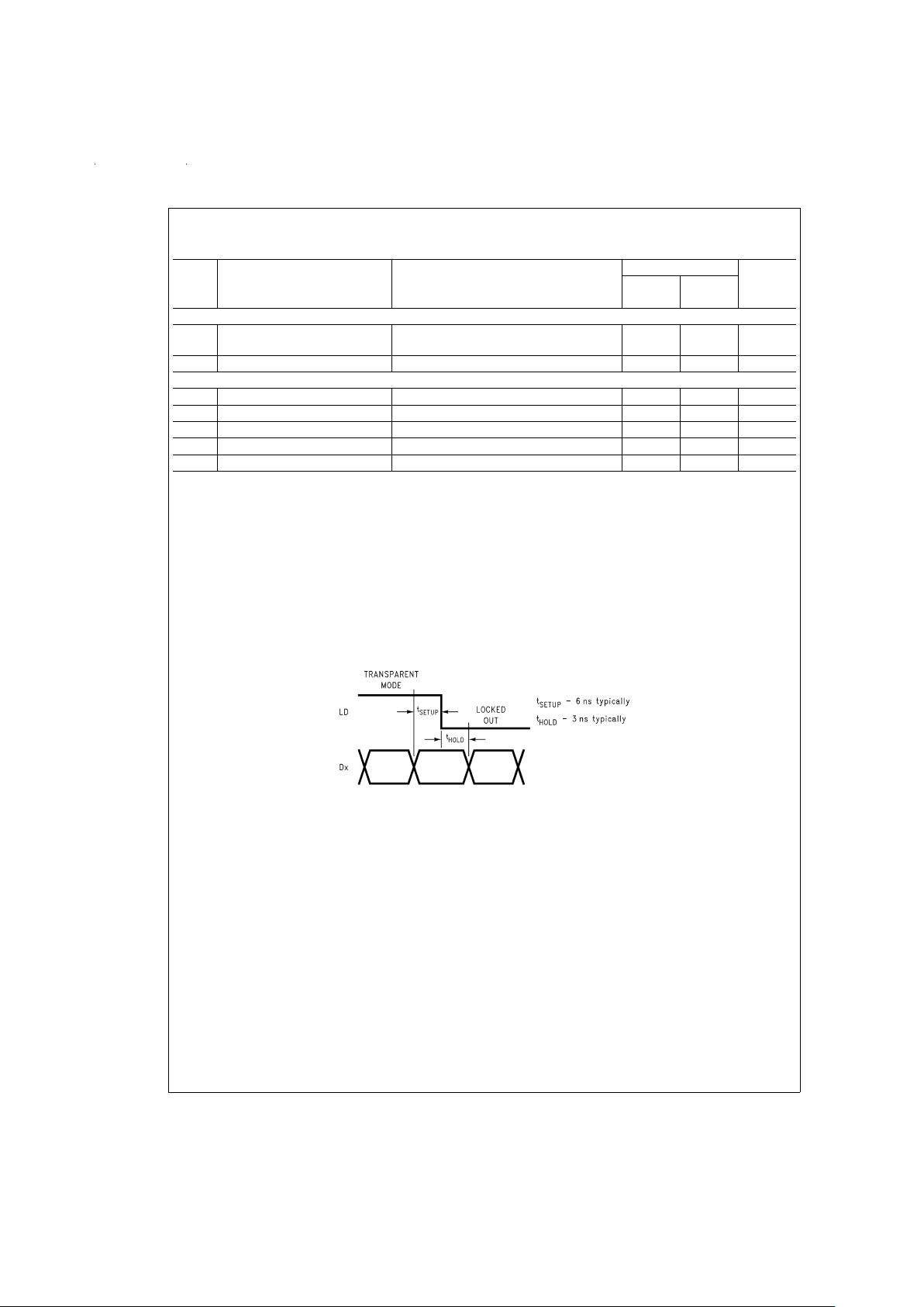
Timing Diagram
DS012677-3
www.national.com 4
Computer Application Circuit
DS012677-4
FIGURE 2.
www.national.com5
 Loading...