

LM4820-6
Fixed Gain 1 Watt Audio Power Amplifier
General Description
The LM4820-6 is an audio power amplifier primarily designed for demanding applications in mobile phones and
other portable communication device applications. It is capable of delivering 1 watt of continuous average power to an
8Ω BTL load with less than 1% distortion (THD+N) at 6dB of
BTL gain from a 5V
DC
power supply.
Boomer audio poweramplifiersweredesigned specifically to
provide high quality output power with a minimal amount of
external components. The LM4820-6 does not require input
and gain resistors, output coupling capacitors or bootstrap
capacitors, and therefore is ideally suited for mobile phone
and other low voltage applications where minimal parts
count and low power consumption is a primary requirement.
The LM4820-6 features a low-power consumption shutdown
mode, which is achieved by driving the shutdown pin with
logic low. Additionally, the LM4820-6 features an internal
thermal shutdown protection mechanism.
The LM4820-6 contains advanced pop & click circuitry which
eliminates noises which would otherwise occur during
turn-on and turn-off transitions.
Key Specifications
j
Improved PSRR at 217Hz 62dB
j
Power Output at 5.0V & 1% THD 1.0W(typ.)
j
Power Output at 3.3V & 1% THD 400mW(typ.)
j
Shutdown Current 0.1µA(typ.)
Features
n Fixed 6dB BTL voltage gain
n Available in space-saving packages micro SMD, MSOP
and SOIC
n Ultra low current shutdown mode
n Can drive capacitive loads up to 500 pF
n Improved pop & click circuitry eliminates noises during
turn-on and turn-off transitions
n 2.0 - 5.5V operation
n No output coupling capacitors, snubber networks or
bootstrap capacitors required
n External gain configuration still possible
Applications
n Mobile Phones
n PDAs
n Portable electronic devices
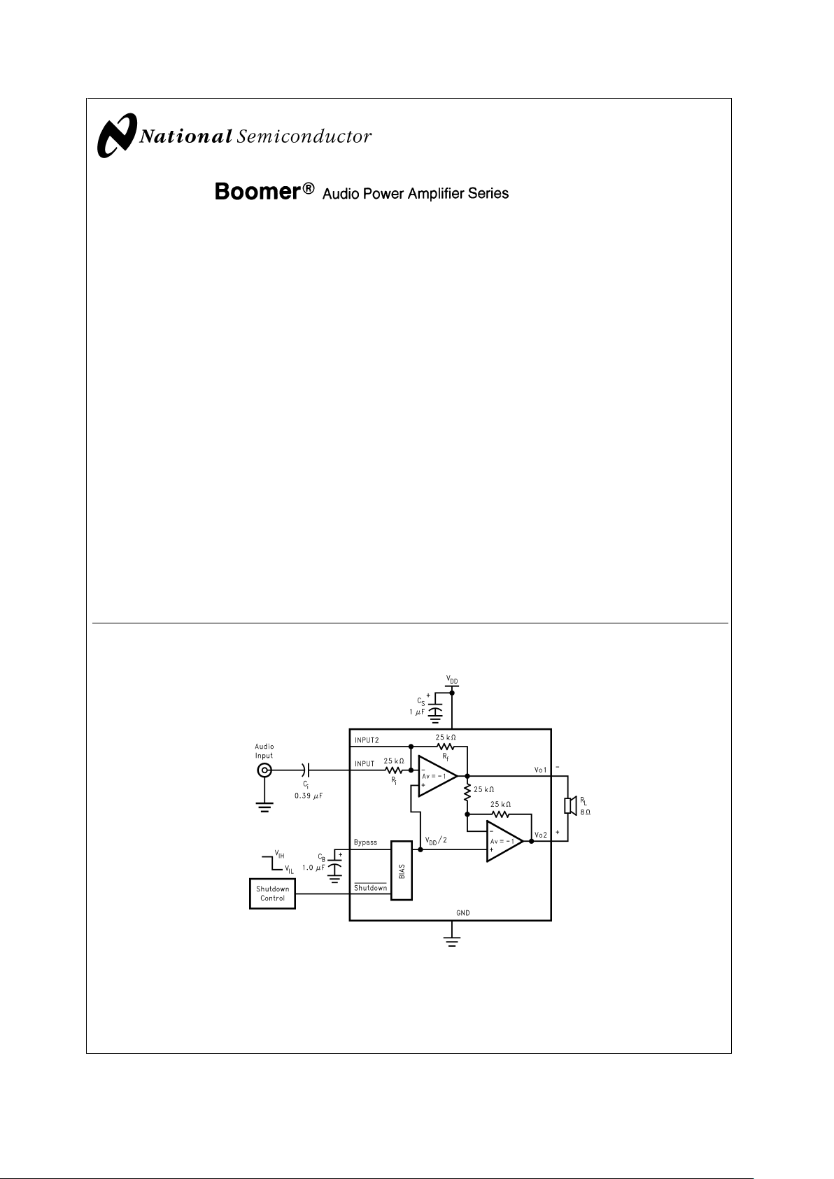
Typical Application
Boomer®is a registered trademark of National Semiconductor Corporation.
DS200106-1
FIGURE 1. Typical Audio Amplifier Application Circuit
April 2002
LM4820-6 Fixed Gain 1 Watt Audio Power Amplifier
© 2002 National Semiconductor Corporation DS200106 www.national.com
Connection Diagram
8 Bump micro SMD
DS200106-23
Top View
Order Number LM4820IBP-6, LM4820IBPX-6
See NS Package Number BPA08DDB
Small Outline (SO) Package
DS200106-35
Top View
Order Number LM4820M-6
See NS Package Number M08A
Mini Small Outline (MSOP) Package
DS200106-36
Top View
Order Number LM4820MM-6
See NS Package Number MUA08A
micro SMD Marking
DS200106-70
Top View
X - Date Code
T - Die Traceability
G - Boomer Family
F - LM4820IBP-6
SO Marking
DS200106-72
Top View
XY - Date Code
TT - Die Traceability
Bottom 2 lines - Part Number ( LM4820M-6 )
MSOP Marking
DS200106-71
Top View
G- Boomer Family
26 - LM4820MM-6
LM4820-6
www.national.com 2
Absolute Maximum Ratings (Note 2)
If Military/Aerospace specified devices are required,
please contact the National Semiconductor Sales Office/
Distributors for availability and specifications.
Supply Voltage 6.0V
Storage Temperature −65˚C to +150˚C
Input Voltage −0.3V to V
DD
+0.3V
Power Dissipation (Note 3) Internally Limited
ESD Susceptibility (Note 4) 2500V
ESD Susceptibility (Note 5) 250V
Junction Temperature 150˚C
Thermal Resistance
θ
JC
(SO) 35˚C/W
θ
JA
(SO) 150˚C/W
θ
JA
(micro SMD) 220˚C/W
θ
JC
(MSOP) 56˚C/W
θ
JA
(MSOP) 190˚C/W
Soldering Information
See AN-1112 ’microSMD Wafers Level Chip Scale
Package’.
Operating Ratings
Temperature Range
T
MIN
≤ TA≤ T
MAX
−40˚C ≤ TA≤ 85˚C
Supply Voltage 2.0V ≤ V
DD
≤ 5.5V
Electrical Characteristics VDD=5V(Notes 1, 2, 8)
The following specifications apply for V
DD
= 5V, AV= 1, and 8Ω load unless otherwise specified. Limits apply for TA= 25˚C.
Symbol Parameter Conditions
LM4820-6
UnitsTypical Limit
(Note 6) (Note 7)
I
DD
Quiescent Power Supply Current VIN= 0V, Io= 0A 4 10 mA (max)
I
SD
Shutdown Current V
shutdown
= GND 0.1 µA (max)
P
o
Output Power THD = 2% (max);f=1kHz 1 W
THD+N Total Harmonic Distortion+Noise P
o
= 0.4 Wrms; f = 1kHz 0.1 %
PSRR Power Supply Rejection Ratio V
ripple
= 200mV sine p-p 62 (f =
217Hz)
66 (f =
1kHz)
dB
A
V
Fixed Voltage Gain 1.41Vinrms, RL=8Ω 6.0 6.5
5.5
dB Max
dB Min
Electrical Characteristics VDD= 3.3V (Notes 1, 2, 8)
The following specifications apply for V
DD
= 3.3V, AV= 1, and 8Ω load unless otherwise specified. Limits apply for TA= 25˚C.
Symbol Parameter Conditions
LM4820-6
UnitsTypical Limit
(Note 6) (Note 7)
I
DD
Quiescent Power Supply Current VIN= 0V, Io= 0A 3.5 mA (max)
I
SD
Shutdown Current V
shutdown
= GND 0.1 µA (max)
P
o
Output Power THD = 1% (max); f = 1kHz 0.4 W
THD+N Total Harmonic Distortion+Noise P
o
= 0.15Wrms; f = 1kHz 0.1 %
PSRR Power Supply Rejection Ratio V
ripple
= 200mV sine p-p 60 (f =
217Hz)
62 (f =
1kHz)
dB
A
V
Fixed Voltage Gain .7Vinrms, RL=8Ω 6.0 dB
LM4820-6
www.national.com3
Electrical Characteristics VDD= 2.6V (Notes 1, 2, 8)
The following specifications apply for V
DD
= 2.6V and 8Ω Load unless otherwise specified. Limits apply for TA= 25˚C.
Symbol Parameter Conditions
LM4820-6
UnitsTypical Limit
(Note 6) (Note 7)
I
DD
Quiescent Power Supply Current VIN= 0V, Io= 0A 2.6 mA (max)
I
SD
Shutdown Current V
shutdown
= GND 0.1 µA (max)
P
0
Output Power ( 8Ω )
Output Power ( 4Ω )
THD = 1% (max);f=1kHzTHD
= 1% (max);f=1kHz
0.2
0.4
W
W
THD+N Total Harmonic Distortion+Noise P
o
= 0.1Wrms; f = 1kHz 0.08 %
PSRR Power Supply Rejection Ratio V
ripple
= 200mV sine p-p 44 (f =
217Hz)
44 (f =
1kHz)
dB
A
V
Fixed Voltage Gain .5Vinrms, RL=8Ω 6.0 dB
Note 1: All voltages are measured with respect to the ground pin, unless otherwise specified.
Note 2:
Absolute Maximum Ratings
indicate limits beyond which damage to the device may occur.
Operating Ratings
indicate conditions for which the device is
functional, but do not guarantee specific performance limits.
Electrical Characteristics
state DC and AC electrical specifications under particular test conditions which
guarantee specific performance limits. This assumes that the device is within the Operating Ratings. Specifications are not guaranteed for parameters where no limit
is given, however, the typical value is a good indication of device performance.
Note 3: The maximum power dissipation must be derated at elevated temperatures and is dictated by T
JMAX
, θJA, and the ambient temperature TA. The maximum
allowable power dissipation is P
DMAX
=(T
JMAX–TA
)/θJAor the number given in Absolute Maximum Ratings, whichever is lower. For the LM4820-6, see power
derating curves for additional information.
Note 4: Human body model, 100 pF discharged through a 1.5 kΩ resistor.
Note 5: Machine Model, 220 pF–240 pF discharged through all pins.
Note 6: Typicals are measured at 25˚C and represent the parametric norm.
Note 7: Limits are guaranteed to National’s AOQL (Average Outgoing Quality Level).
Note 8: For micro SMD only, shutdown current is measured in a Normal Room Environment. Exposure to direct sunlight will increase I
SD
by a maximum of 2µA.
External Components Description (
Figure 1
)
Components Functional Description
2. C
i
Input coupling capacitor which blocks the DC voltage at the amplifiers input terminals. Also creates a
highpass filter with R
i
at fc= 1/(2π RiCi). Refer to the section, Proper Selection of External Components,
for an explanation of how to determine the value of C
i
.
4. C
S
Supply bypass capacitor which provides power supply filtering. Refer to the Power Supply Bypassing
section for information concerning proper placement and selection of the supply bypass capacitor.
5. C
B
Bypass pin capacitor which provides half-supply filtering. Refer to the section, Proper Selection of External
Components, for information concerning proper placement and selection of C
B
.
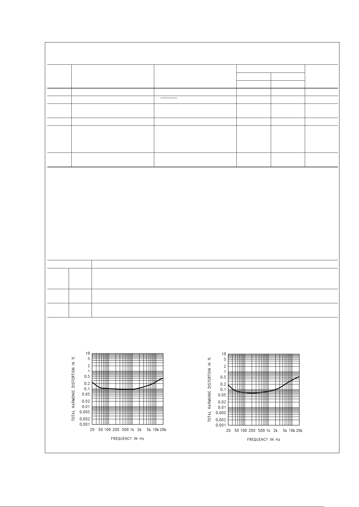
Typical Performance Characteristics
THD+N vs Frequency
at V
DD
=5V,8ΩRL, and PWR = 250mW
DS200106-37
THD+N vs Frequency
at V
DD
= 3.3V, 8Ω RL, and PWR = 150mW
DS200106-38
LM4820-6
www.national.com 4
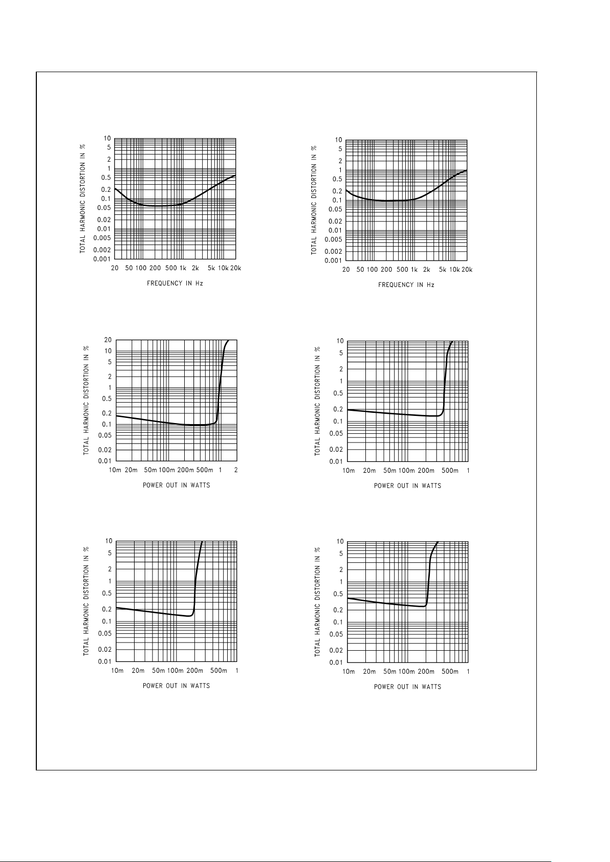
Typical Performance Characteristics (Continued)
THD+N vs Frequency
at V
DD
= 2.6V, 8Ω RL, and PWR = 100mW
DS200106-39
THD+N vs Frequency
at V
DD
= 2.6V, 4Ω RL, and PWR = 100mW
DS200106-40
THD+N vs Power Out
@
VDD=5V,8ΩRL, 1kHz
DS200106-41
THD+N vs Power Out
@
VDD= 3.3V, 8Ω RL, 1kHz
DS200106-42
THD+N vs Power Out
@
VDD= 2.6V, 8Ω RL, 1kHz
DS200106-43
THD+N vs Power Out
@
VDD= 2.6V, 4Ω RL, 1kHz
DS200106-44
LM4820-6
www.national.com5
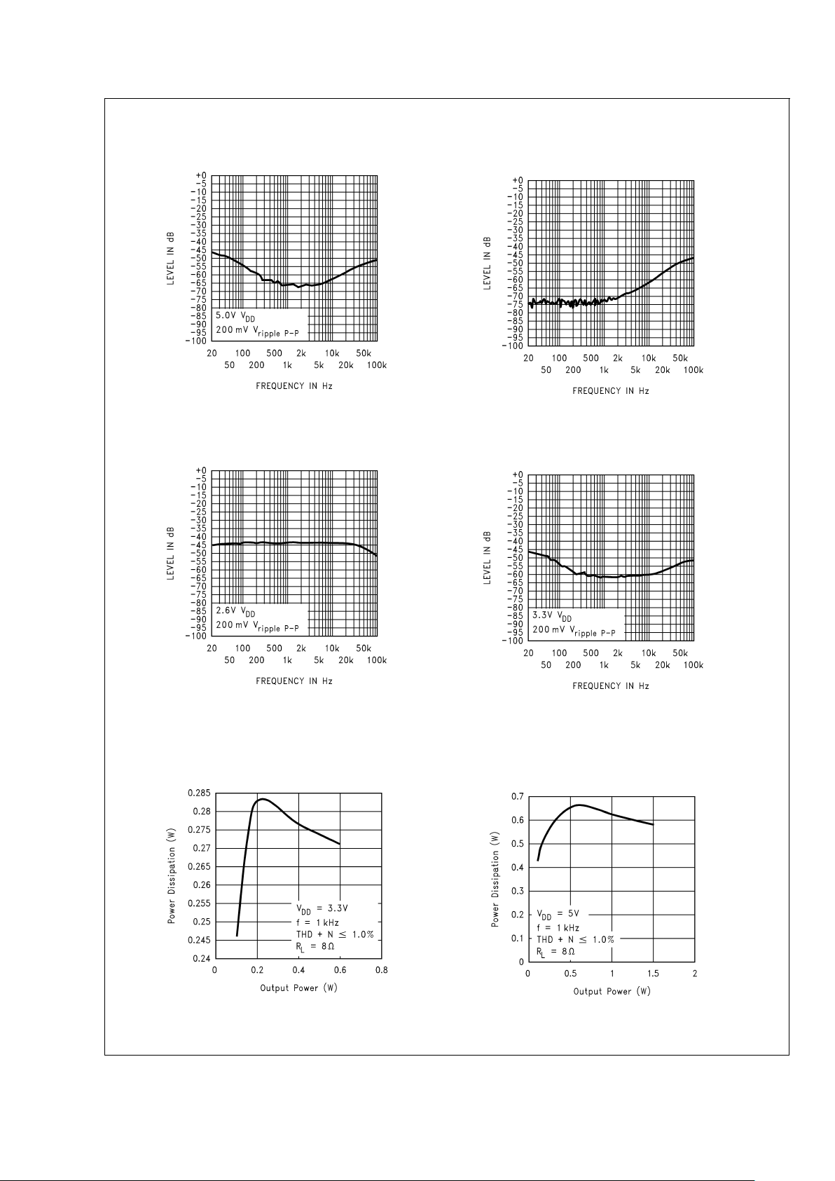
Typical Performance Characteristics (Continued)
Power Supply Rejection Ratio (PSRR)
@
VDD=5V
DS200106-45
Input terminated with 10Ω R
Power Supply Rejection Ratio (PSRR)
@
VDD=5V
DS200106-73
Input Floating
Power Supply Rejection Ratio (PSRR)
@
VDD= 2.6V
DS200106-47
Input terminated with 10Ω R
Power Supply Rejection Ratio (PSRR)
@
VDD= 3.3V
DS200106-46
Input terminated with 10Ω R
Power Dissipation vs
Output Power
V
DD
= 3.3V
DS200106-49
Power Dissipation vs
Output Power
@
VDD=5V
DS200106-48
LM4820-6
www.national.com 6
 Loading...