

NSC LM4819MX, LM4819MMX, LM4819MM, LM4819LDX, LM4819M Datasheet
LM4819
350mW Audio Power Amplifier with Shutdown Mode
General Description
The LM4819 is a mono bridged power amplifier that is capable of delivering 350mW
RMS
output power into a 16Ω load
or 300mW
RMS
output power into an 8Ω load with 10%
THD+N from a 5V power supply.
The LM4819 Boomer audio power amplifier is designed
specifically to provide high quality output power and minimize PCB area with surface mount packaging and a minimal
amount of external components. Since the LM4819 doesnot
require output coupling capacitors, bootstrap capacitors or
snubber networks, it is optimally suited for low-power portable applications.
The closed loop response of the unity-gain stable LM4819
can be configured using external gain-setting resistors. The
device is available in LLP, MSOP, and SO package types to
suit various applications.
Key Specifications
n THD+N at 1kHz, 350mW continuous average output
power into 16Ω 10% (max)
n THD+N at 1kHz, 300mW continuous average output
power into 8Ω 10% (max)
n Shutdown Current 0.7µA (typ)
Features
n LLP, SOP, and MSOP surface mount packaging.
n Switch on/off click suppression.
n Unity-gain stable.
n Minimum external components.
Applications
n General purpose audio
n Portable electronic devices
n Information Appliances (IA)
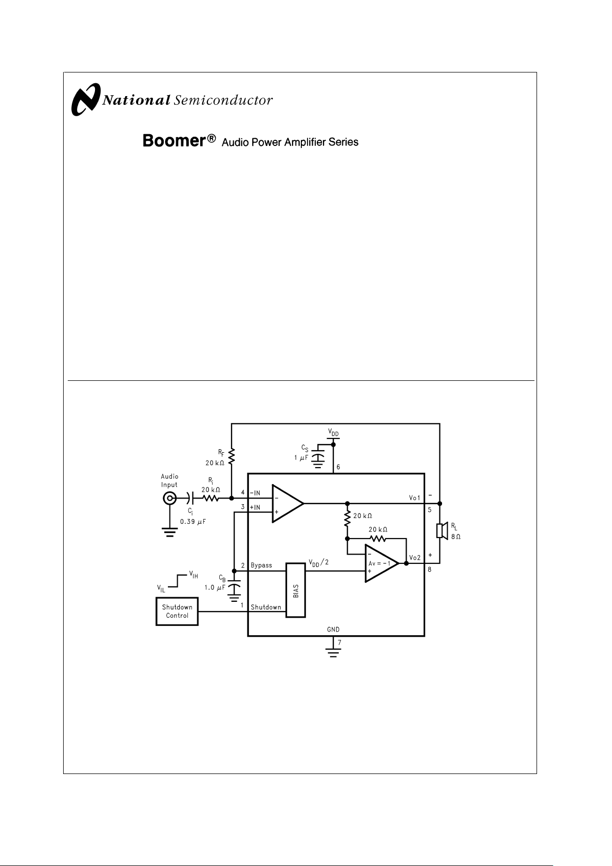
Typical Application
Boomer®is a registered trademark of National Semiconductor Corporation.
DS200136-1
FIGURE 1. Typical Audio Amplifier Application Circuit
April 2002
LM4819 350mW Audio Power Amplifier with Shutdown Mode
© 2002 National Semiconductor Corporation DS200136 www.national.com
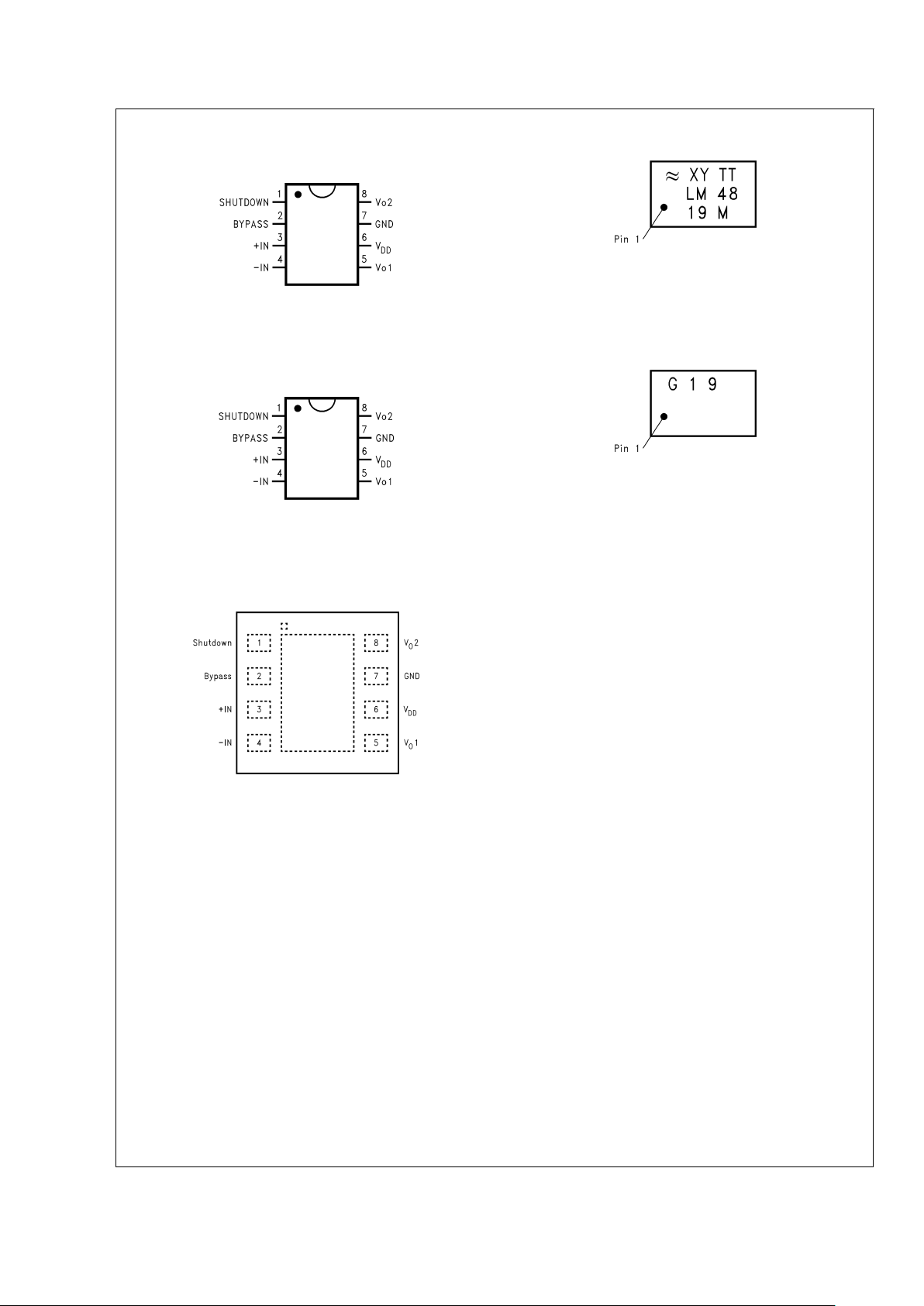
Connection Diagrams
Small Outline (SO) Package
DS200136-35
Top View
Order Number LM4819M
See NS Package Number M08A
Mini Small Outline (MSOP) Package
DS200136-36
Top View
Order Number LM4819MM
See NS Package Number MUA08A
LLP Package
DS200136-74
Top View
Order Number LM4819LD
See NS Package Number LDA08B
SO Marking
DS200136-72
Top View
XY - Date Code
TT - Die Traceability
Bottom 2 lines - Part Number
MSOP Marking
DS200136-71
Top View
G - Boomer Family
19 - LM4819MM
LM4819
www.national.com 2
Absolute Maximum Ratings (Notes 2, 3)
If Military/Aerospace specified devices are required,
please contact the National Semiconductor Sales Office/
Distributors for availability and specifications.
Supply Voltage 6.0V
Storage Temperature −65˚C to +150˚C
Input Voltage −0.3V to V
DD
+0.3V
Power Dissipation (P
D
) (Note 4) Internally Limited
ESD Susceptibility (Note 5) 3.5kV
ESD Susceptibility (Note 6) 250V
Junction Temperature (T
J
) 150˚C
Soldering Information (Note 1)
Small Outline Package
Vapor Phase (60 seconds) 215˚C
Infrared (15 seconds) 220˚C
Thermal Resistance
θ
JC
(MSOP) 56˚C/W
θ
JA
(MSOP) 210˚C/W
θ
JC
(SOP) 35˚C/W
θ
JA
(SOP) 170˚C/W
θ
JA
(LLP) 117˚C/W (Note 10)
θ
JA
(LLP) 150˚C/W (Note 11)
Operating Ratings (Notes 2, 3)
Temperature Range
T
MIN
≤ TA≤ T
MAX
−40˚C ≤ TA≤ 85˚C
Supply Voltage 2.0V ≤ V
CC
≤ 5.5V
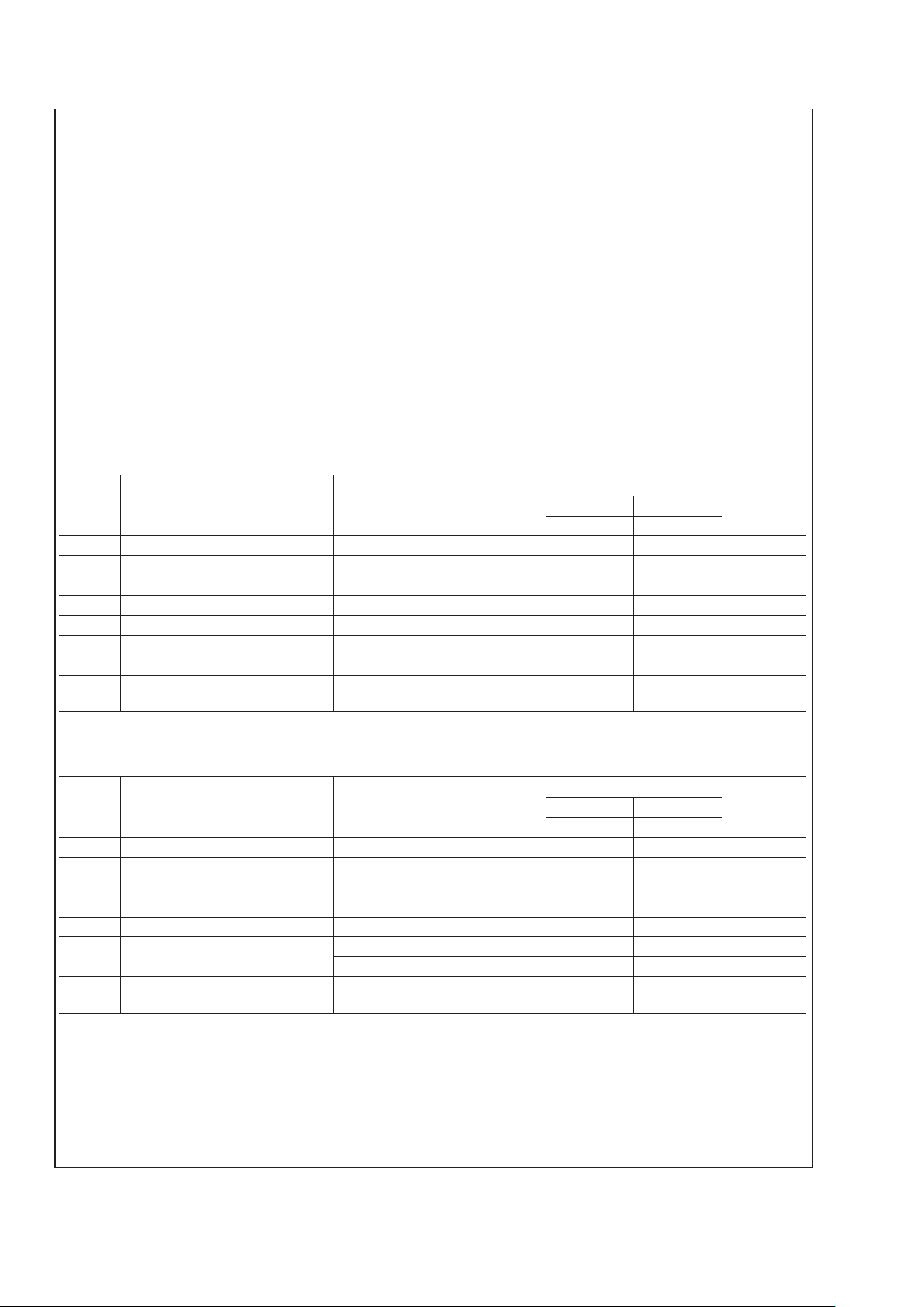
Electrical Characteristics VDD=5V(Notes 2, 3)
The following specifications apply for V
DD
= 5V, RL=16Ωunless otherwise stated. Limits apply for TA= 25˚C.
Symbol Parameter Conditions
LM4819
Units
(Limits)
Typical Limit
(Note 7) (Notes 8, 9)
I
DD
Quiescent Power Supply Current VIN= 0V, Io= 0A 1.5 3.0 mA (max)
I
SD
Shutdown Current V
PIN1=VDD
(Note 12) 1.0 5.0 µA (max)
V
SDIH
Shutdown Voltage Input High 4.0 V (min)
V
SDIL
Shutdown Voltage Input Low 1.0 V (max)
V
OS
Output Offset Voltage VIN= 0V 5 50 mV (max)
P
O
Output Power
THD = 10%, f
IN
= 1kHz 350 mW
THD = 10%, f
IN
= 1kHz, RL=8Ω 300 mW
THD+N Total Harmonic Distortion + Noise P
O
= 270mW
RMS,AVD
=2,fIN=
1kHz
1%
Electrical Characteristics VDD=3V(Notes 2, 3)
The following specifications apply for V
DD
= 3V and RL=16Ωload unless otherwise stated. Limits apply to TA= 25˚C.
Symbol Parameter Conditions
LM4819
Units
(Limits)
Typical Limit
(Note 7) (Notes 8, 9)
I
DD
Quiescent Power Supply Current VIN= 0V, Io= 0A 1.0 3.0 mA (max)
I
SD
Shutdown Current V
PIN1=VDD
(Note 12) 0.7 5.0 µA (max)
V
SDIH
Shutdown Voltage Input High 2.4 V (min)
V
SDIL
Shutdown Voltage Input Low 0.6 V (max)
V
OS
Output Offset Voltage VIN= 0V 5 50 mV
P
O
Output Power
THD = 10%, f
IN
= 1kHz 110 mW
THD = 10%, f
IN
= 1kHz, RL=8Ω 90 mW
THD+N Total Harmonic Distortion + Noise P
O
= 80mW
RMS,AVD
=2,fIN=
1kHz
1%
LM4819
www.national.com3
Electrical Characteristics VDD=3V(Notes 2, 3)
The following specifications apply for V
DD
= 3V and RL=16Ωload unless otherwise stated. Limits apply to TA=
25˚C. (Continued)
Note 1: See AN-450 ’Surface Mounting and their Effects on Product Reliability’ for other methods of soldering surface mount devices.
Note 2: All voltages are measured with respect to the ground pin, unless otherwise specified.
Note 3:
Absolute Maximum Ratings
indicate limits beyond which damage to the device may occur.
Operating Ratings
indicate conditions for which the device is
functional, but do not guarantee specific performance limits.
Electrical Characteristics
state DC and AC electrical specifications under particular test conditions which
guarantee specific performance limits. This assumes that the device is within the Operating Ratings. Specifications are not guaranteed for parameters where no limit
is given. However, the typical value is a good indication of device’s performance.
Note 4: The maximum power dissipation must be derated at elevated temperatures and is dictated by T
JMAX
, θJA, and the ambient temperature TA. The maximum
allowable power dissipation is P
DMAX
=(T
JMAX–TA
)/θJA. For the LM4819, T
JMAX
= 150˚C and the typical junction-to-ambient thermal resistance (θJA) when board
mounted is 210˚C/W for the MSOP package and 170˚C/W for the SOP package.
Note 5: Human body model, 100pF discharged through a 1.5 kΩ resistor.
Note 6: Machine Model, 220pF–240pF capacitor is discharged through all pins.
Note 7: Typical specifications are specified at 25˚C and represent the parametric norm.
Note 8: Tested limits are guaranteed to National’s AOQL (Average Outgoing Quality Level).
Note 9: Datasheet min/max specification limits are guaranteed by designs, test, or statistical analysis.
Note 10: The given θ
JA
is for an LM4819 package in an LDA08B with the Exposed-DAP soldered to a printed circuit board copper pad with an area equivalent to
that of the Exposed-DAP itself. The Exposed-DAP of the LDA08B package should be electrically connected to GND or an electrically isolated copper area.
Note 11: The given θ
JA
is for an LM4819 package in an LDA08B with the Exposed-DAP not soldered to any printed circuit board copper.
Note 12: The shutdown pin (pin1) should be driven as close as possible to V
DD
for minimum current in Shutdown Mode.
External Components Description (
Figure 1
)
Components Functional Description
1. R
i
Combined with Rf, this inverting input resistor sets the closed-loop gain. Rialso forms a high pass filter with
C
i
at fc= 1/(2πRiCi).
2. C
i
This input coupling capacitor blocks DC voltage at the amplifier’s terminals. Combined with Ri, it creates a
high pass filter with R
i
at fc= 1/(2πRiCi). Refer to the section, Proper Selection of External Components
for an explanation of how to determine the value of C
i
.
3. R
f
Combined with Ri, this is the feedback resistor that sets the closed-loop gain: Av= 2(RF/Ri).
4. C
S
This is the power supply bypass capacitor that filters the voltage applied to the power supply pin. Refer to
the Application Information section for proper placement and selection of C
s
.
5. C
B
This is the bypass pin capacitor that filters the voltage at the BYPASS pin. Refer to the section, Proper
Selection of External Components, for information concerning proper placement and selection of C
B
.
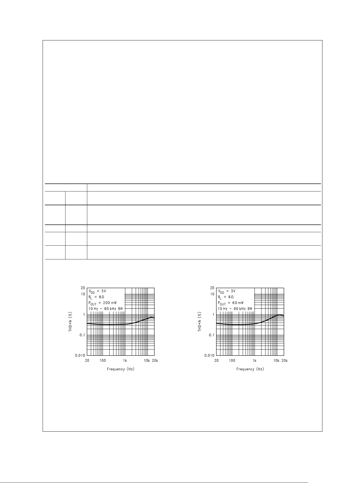
Typical Performance Characteristics
THD+N vs Frequency
DS200136-37
THD+N vs Frequency
DS200136-38
LM4819
www.national.com 4
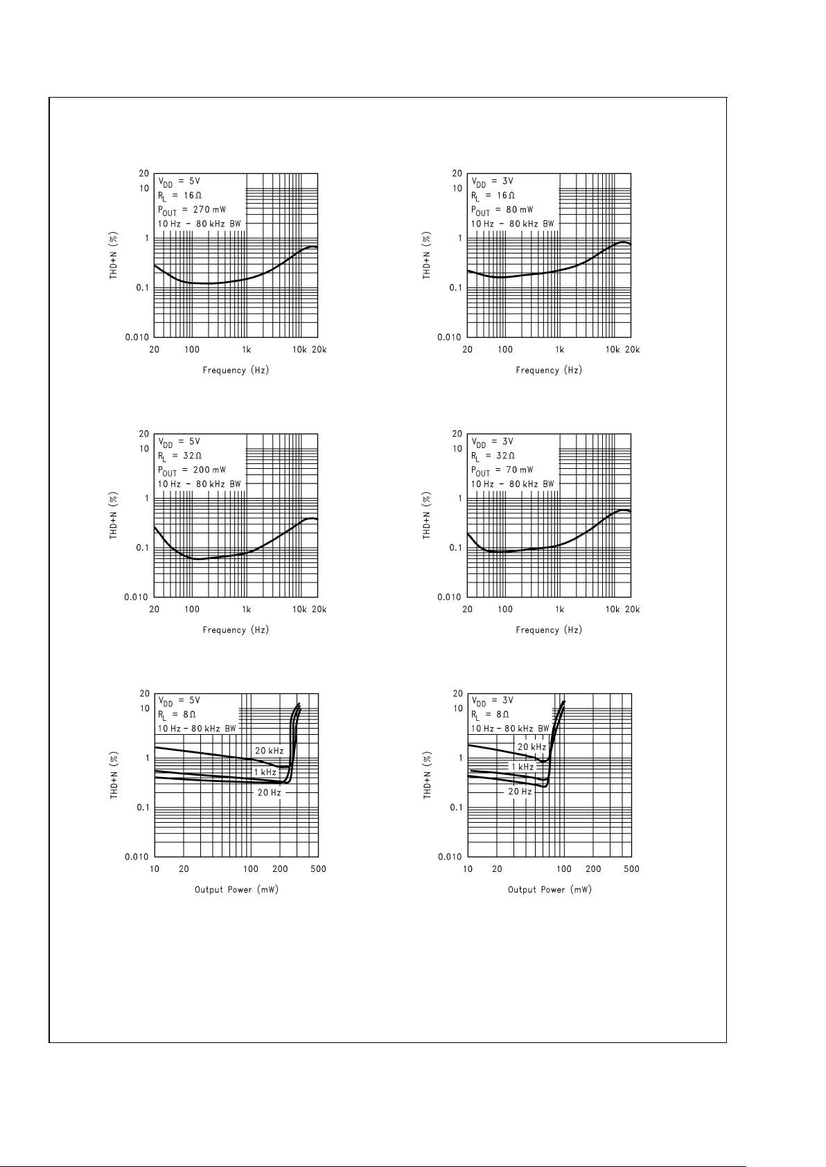
Typical Performance Characteristics (Continued)
THD+N vs Frequency
DS200136-39
THD+N vs Frequency
DS200136-40
THD+N vs Frequency
DS200136-41
THD+N vs Frequency
DS200136-42
THD+N vs Output Power
DS200136-43
THD+N vs Output Power
DS200136-44
LM4819
www.national.com5
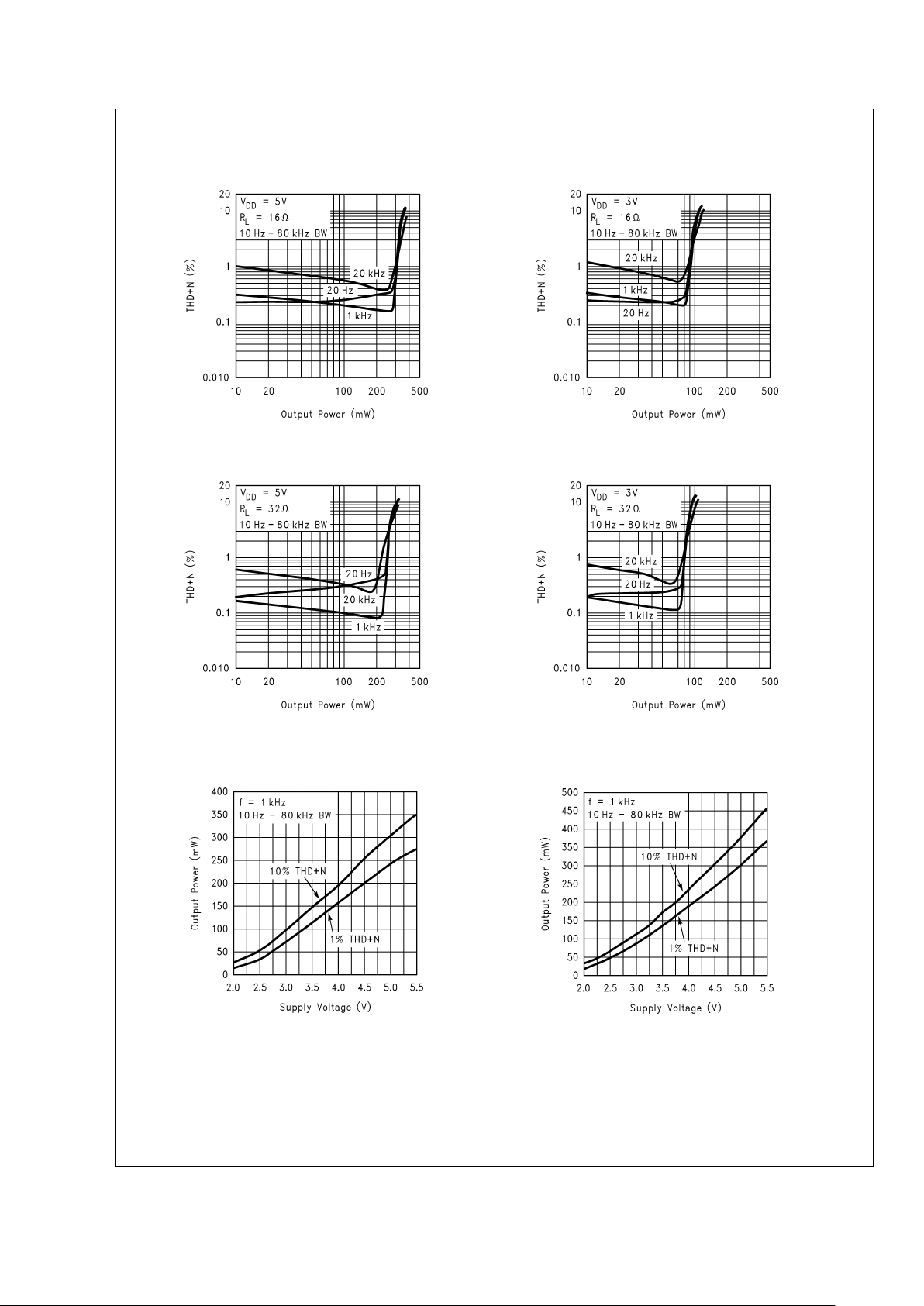
Typical Performance Characteristics (Continued)
THD+N vs Output Power
DS200136-45
THD+N vs Output Power
DS200136-73
THD+N vs Output Power
DS200136-47
THD+N vs Output Power
DS200136-46
Output Power vs Supply Voltage
R
L
=8Ω
DS200136-49
Output Power vs Supply Voltage
R
L
=16Ω
DS200136-48
LM4819
www.national.com 6
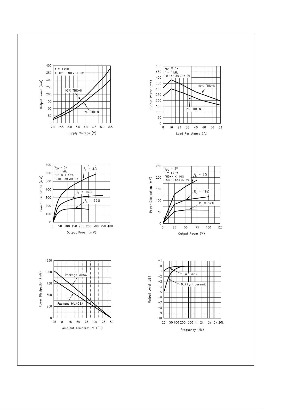
Typical Performance Characteristics (Continued)
Output Power vs Supply Voltage
R
L
=32Ω
DS200136-51
Output Power vs Load Resistance
DS200136-50
Power Dissipation vs
Output Power
V
DD
=5V
DS200136-53
Power Dissipation vs
Output Power
V
DD
=3V
DS200136-52
Power Derating Curves
DS200136-55
Frequency Response vs
Input Capacitor Size
DS200136-54
LM4819
www.national.com7
 Loading...