

NSC LM4811MM, LM4811LDX, LM4811LD Datasheet
LM4811
Dual 105mW Headphone Amplifier with Digital Volume
Control and Shutdown Mode
General Description
The LM4811 is a dual audio power amplifier capable of
delivering 105mW per channel of continuous average power
into a 16Ω load with 0.1% (THD+N) from a 5V power supply.
Boomer audio power amplifiers were designed specifically to
provide high quality output power with a minimal amount of
external components. Since the LM4811 does not require
bootstrap capacitors or snubber networks, it is optimally
suited for low-power portable systems.
The LM4811 features a digital volume control that sets the
amplifier’s gain from +12dB to −33dB in 16 discrete steps
using a two−wire interface.
The unity-gain stable LM4811 also features an externally
controlled, active-high, micropower consumption shutdown
mode. It also has an internal thermal shutdown protection
mechanism.
Key Specifications
n THD+N at 1kHz, 105mW continuous average output
power into 16Ω 0.1% (typ)
n THD+N at 1kHz, 70mW continuous average power into
32Ω 0.1% (typ)
n Shutdown Current 0.3µA (typ)
Features
n Digital volume control range from +12dB to −33dB
n LD and MSOP surface mount packaging
n "Click and Pop" suppression circuitry
n No bootstrap capacitors required
n Low shutdown current
Applications
n Cellular Phones
n MP3, CD, DVD players
n PDA’s
n Portable electronics
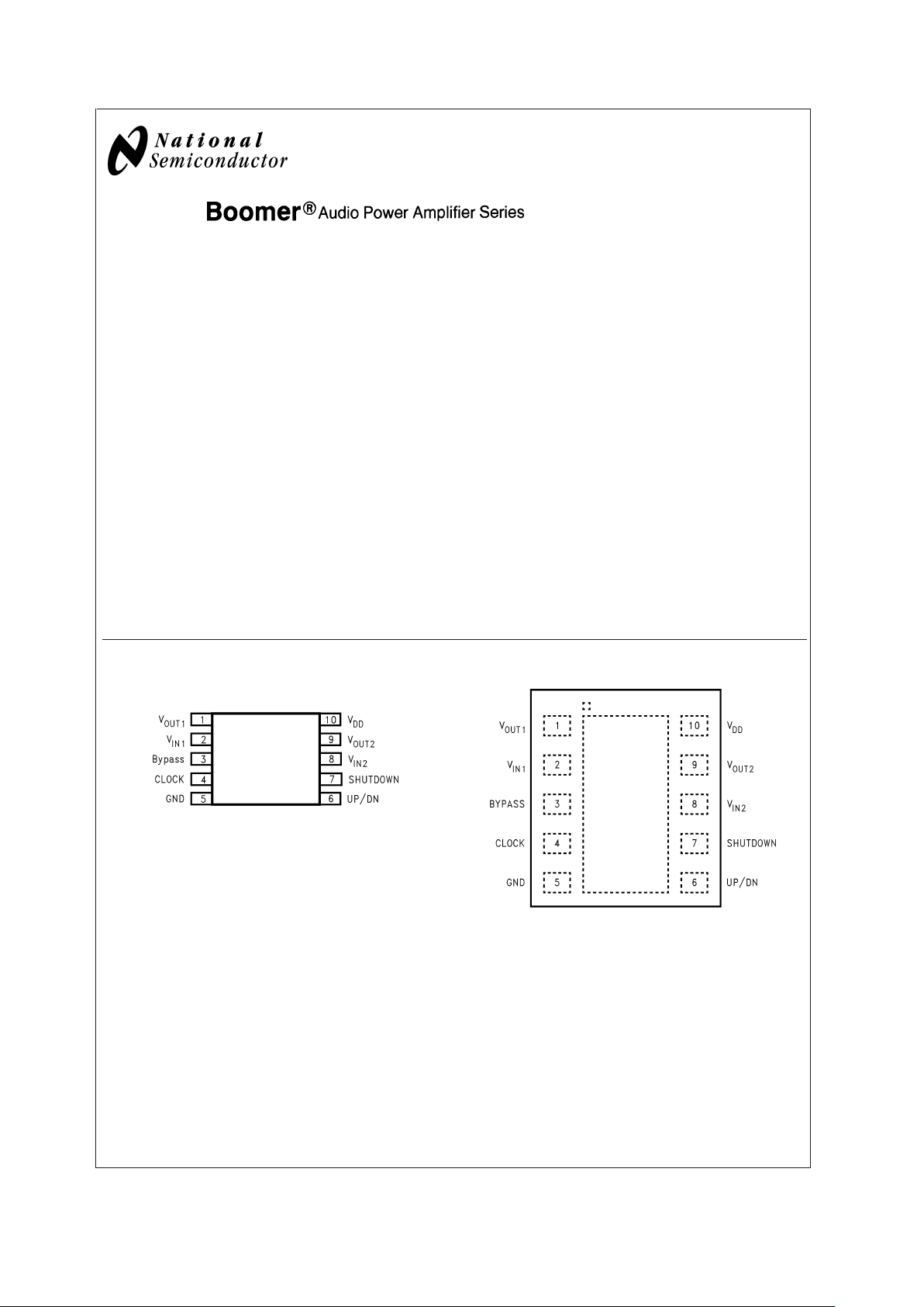
Connection Diagrams
MSOP Package
20006102
Top View
Order Number LM4811MM
See NS Package Number MUB10A
LD Package
20006162
Top View
Order Number LM4811LD
See NS Package Number LDA10A
Boomer®is a registered trademark of National Semiconductor Corporation.
December 2002
LM4811 Dual 105mW Headphone Amplifier with Digital Volume Control and Shutdown Mode
© 2002 National Semiconductor Corporation DS200061 www.national.com
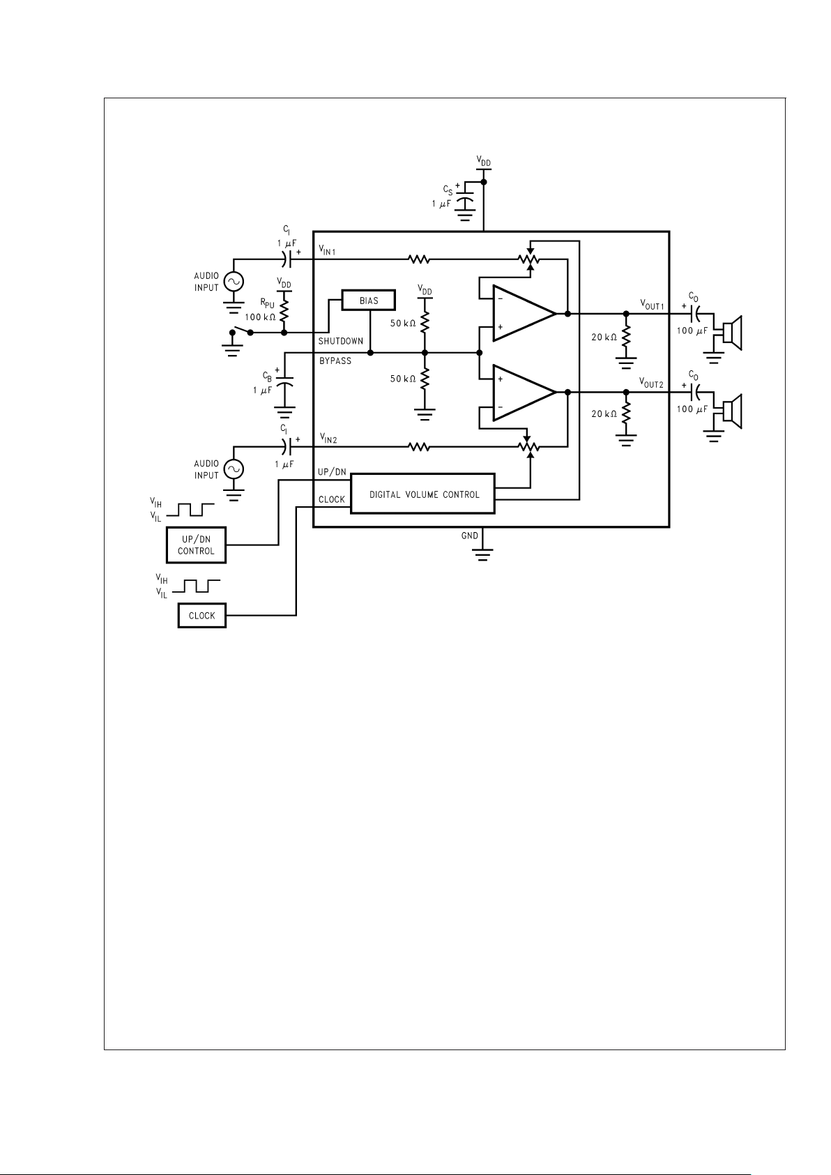
Typical Application
20006101
*Refer to the Application Information Section for information concerning proper selection of the input and output coupling capacitors.
FIGURE 1. Typical Audio Amplifier Application Circuit
LM4811
www.national.com 2
Absolute Maximum Ratings (Note 1)
If Military/Aerospace specified devices are required,
please contact the National Semiconductor Sales Office/
Distributors for availability and specifications.
Supply Voltage 6.0V
Storage Temperature −65˚C to +150˚C
ESD Susceptibility (Note 3) 2.5kV
ESD Susceptibility Machine model
(Note 6) 200V
Junction Temperature (T
J
) 150˚C
Soldering Information
Small Outline Package
Vapor Phase (60 sec.) 215˚C
Infrared (15 sec.) 220˚C
Thermal Resistance
θ
JA
MUB10A 194˚C/W
θ
JC
MUB10A 52˚C/W
θ
JA
LDA10A (Note 7) 63˚C/W
θ
JC
LDA10A (Note 7) 12˚C/W
Operating Ratings
Temperature Range
T
MIN
≤ TA≤ T
MAX
−40˚C ≤ TA≤ 85˚C
Supply Voltage 2.0V ≤ V
CC
≤ 5.5V
Electrical Characteristics (Notes 1, 8)
The following specifications apply for VDD= 5V unless otherwise specified, limits apply to TA= 25˚C.
Symbol Parameter Conditions LM4811 Units
(Limits)
Typical
(Note 4)
Limit
(Note 5)
V
DD
Supply Voltage 2.0 V (min)
5.5 V (max)
I
DD
Supply Current VIN= 0V, IO= 0A 1.3 3.0 mA
I
SD
Shutdown Current VIN= 0V 0.3 µA
V
OS
Output Offset Voltage VIN= 0V 4.0 50 mV
P
O
Output Power 0.1% THD+N; f = 1kHz
R
L
=16Ω 105 mW
R
L
=32Ω 70 mW
THD+N Total Harmonic Distortion P
O
= 50mW, RL=32Ω
f = 20Hz to 20kHz
0.3 %
Crosstalk Channel Separation R
L
=32Ω; f = 1kHz;
P
O
= 70mW
100 dB
PSRR Power Supply Rejection Ratio C
B
= 1.0µF, V
RIPPLE
= 100mV
PP
f = 217Hz
60 dB
V
IH
(CLOCK, UP/DN, SHUTDOWN)
Input Voltage High
1.4 V (min)
V
IL
(CLOCK, UP/DN, SHUTDOWN)
Input Voltage Low
0.4 V (max)
Digital Volume Range Input referred minimum gain −33 dB
Input referred maximum gain +12 dB
Digital Volume Stepsize All 16 discrete steps 3.0 dB
Stepsize Error All 16 discrete steps
±
0.3 dB
Channel−to−Channel Volume
Tracking Error
All gain settings from
−33dB to +12dB
0.15 dB
Shutdown Attenuation Shutdown mode active −100 dB
LM4811
www.national.com3
Electrical Characteristics (Notes 1, 8)
The following specifications apply for VDD= 3.3V unless otherwise specified, limits apply to TA= 25˚C.
Symbol Parameter Conditions LM4811 Units
(Limits)
Typical
(Note 4)
Limit
(Note 5)
I
DD
Supply Current VIN= 0V, IO= 0A 1.1 mA
I
SD
Shutdown Current VIN= 0V 0.3 µA
V
OS
Output Offset Voltage VIN= 0V 4.0 mV
P
o
Output Power 0.1% THD+N; f = 1kHz
R
L
=16Ω 40 mW
R
L
=32Ω 28 mW
THD+N Total Harmonic Distortion P
O
= 25mW, RL=32Ω
f = 20Hz to 20kHz
0.5 %
PSRR Power Supply Rejection Ratio C
B
= 1.0µF, V
RIPPLE
= 100mV
PP
f = 217Hz
60 dB
V
IH
(CLOCK, UP/DN, SHUTDOWN)
Input Voltage High
1.4 V (min)
V
IL
(CLOCK, UP/DN, SHUTDOWN)
Input Voltage Low
0.4 V (max)
Digital Volume Range Input referred minimum gain −33 dB
Input referred maximum gain +12 dB
Digital Volume Stepsize All 16 discrete steps 3.0 dB
Stepsize Error All 16 discrete steps
±
0.3 dB
Channel−to−Channel Volume
Tracking Error
All gain settings from
−33dB to +12dB
0.15 dB
Shutdown Attenuation Shutdown mode active −100 dB
Electrical Characteristics (Notes 1, 8)
The following specifications apply for VDD= 2.6V unless otherwise specified, limits apply to TA= 25˚C.
Symbol Parameter Conditions LM4811 Units
(Limits)
Typical
(Note 4)
Limit
(Note 5)
I
DD
Supply Current VIN= 0V, IO= 0A 1.0 mA
I
SD
Shutdown Current VIN= 0V 0.3 µA
V
OS
Output Offset Voltage VIN= 0V 4.0 mV
P
o
Output Power 0.1% THD+N; f = 1kHz
R
L
=16Ω 20 mW
R
L
=32Ω 16 mW
THD+N Total Harmonic Distortion P
O
= 15mW, RL=32Ω
f = 20Hz to 20kHz
0.6 %
PSRR Power Supply Rejection Ratio C
B
= 1.0µF, V
RIPPLE
= 100mV
PP
f = 217Hz
60 dB
V
IH
(CLOCK, UP/DN, SHUTDOWN)
Input Voltage High
1.4 V (min)
V
IL
(CLOCK, UP/DN, SHUTDOWN)
Input Voltage Low
0.4 V (max)
Digital Volume Range Input referred minimum gain −33 dB
Input referred maximum gain +12 dB
Digital Volume Stepsize All 16 discrete steps 3.0 dB
Stepsize Error All 16 discrete steps
±
0.3 dB
Channel−to−Channel Volume
Tracking Error
All gain settings from
−33dB to +12dB
0.15 dB
LM4811
www.national.com 4
Electrical Characteristics (Notes 1, 8) (Continued)
The following specifications apply for VDD= 2.6V unless otherwise specified, limits apply to TA= 25˚C.
Symbol Parameter Conditions LM4811 Units
(Limits)
Typical
(Note 4)
Limit
(Note 5)
Shutdown Attenuation Shutdown mode active −75 dB
Note 1: Absolute Maximum Ratings indicate limits beyond which damage to the device may occur.
Note 2: Operating Ratings indicate conditions for which the device is functional, but do not guarantee specific performance limits. For guaranteed specifications and
test conditions, see the Electrical Characteristics. The guaranteed specifications apply only for the test conditions listed. Some performance characteristics may
degrade when the device is not operated under the listed test conditions.
Note 3: Human body model, 100pF discharged through a 1.5kΩ resistor.
Note 4: Typical specifications are specified at +25˚C and represent the most likely parametric norm.
Note 5: Tested limits are guaranteed to National’s AOQL (Average Outgoing Quality Level). Datasheet min/max specification limits are guaranteed by design, test,
or statistical analysis.
Note 6: : Machine Model ESD test is covered by specification EIAJ IC-121-1981. A 200pF cap is charged to the specified voltage, then discharged directly into the
IC with no external series resistor (resistance of discharge path must be under 50 Ohms).
Note 7: The LDA10A package has its Exposed−DAP soldered to an exposed 2in
2
area of 1oz printed circuit board copper.
Note 8: All voltages are measured with respect to the ground pin, unless otherwise specified.
External Components Description
(Figure 1)
Components Functional Description
1. C
i
This is the input coupling capacitor. It blocks the DC voltage at, and couples the input signal to, the
amplifier’s input terminals. C
i
also creates a highpass filter with the internal input resistor, Ri,atfc=
1/(2πR
iCi
). The minimum value of Riis 33kΩ. Refer to the section, Proper Selection of External
Components, for an explanation of how to determine the value of C
i
.
2. C
S
This is the supply bypass capacitor. It provides power supply filtering. Refer to the Application
Information section for proper placement and selection of the supply bypass capacitor.
3. C
B
This is the BYPASS pin capacitor. It provides half-supply filtering. Refer to the section, Proper
Selection of External Components, for information concerning proper placement and selection of C
B
.
4. C
O
This is the output coupling capacitor. It blocks the DC voltage at the amplifier’s output and it forms a
high pass filter with R
L
at fO= 1/(2πRLCO)
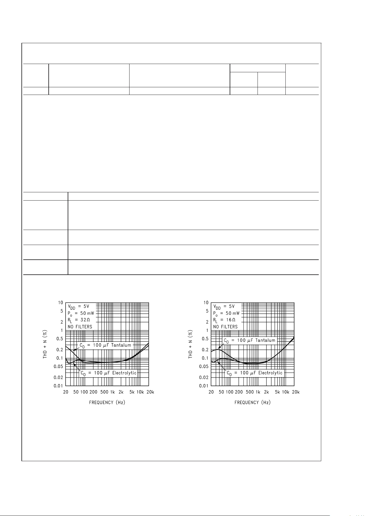
Typical Performance Characteristics
THD+N vs Frequency THD+N vs Frequency
20006103 20006104
LM4811
www.national.com5
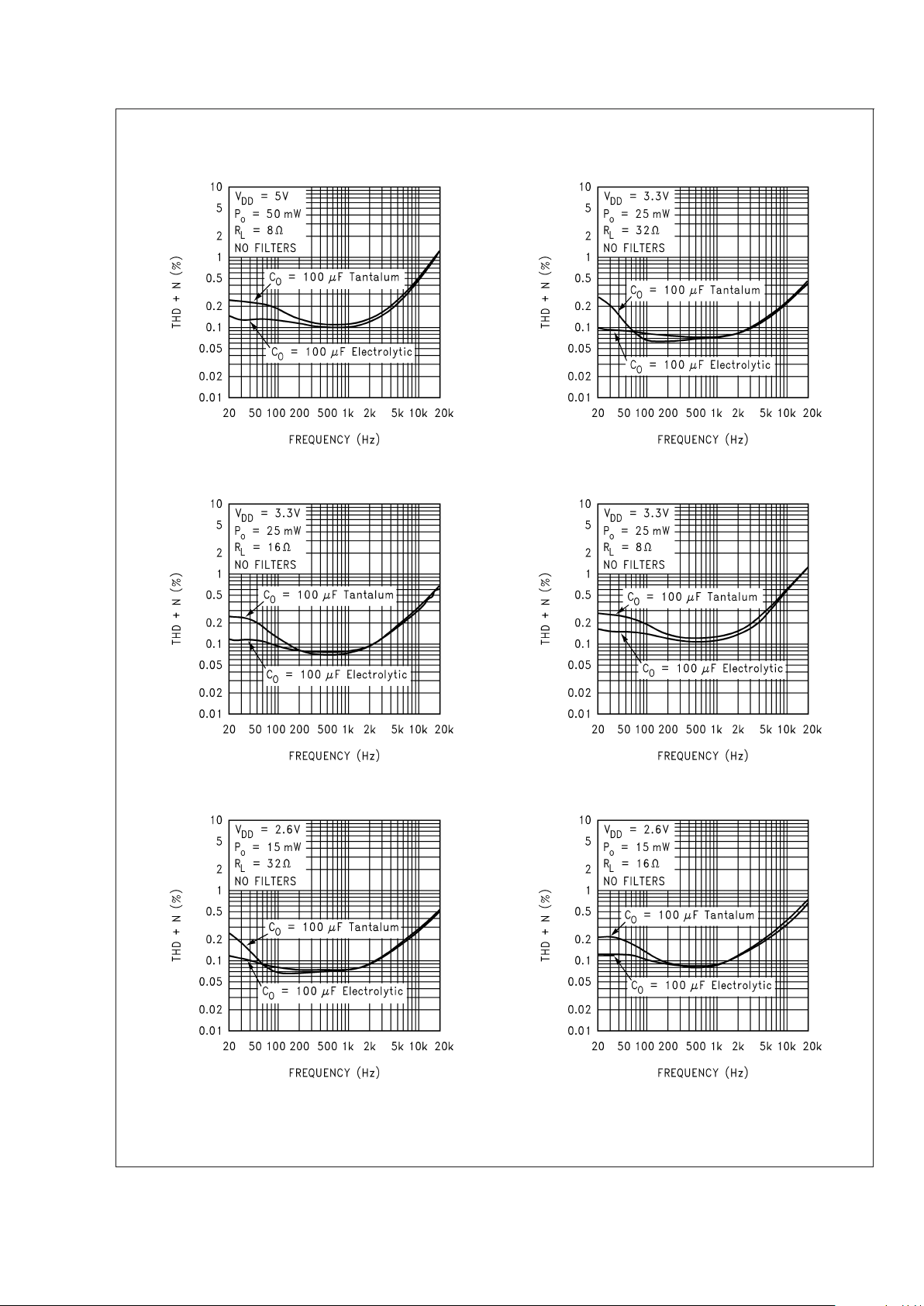
Typical Performance Characteristics (Continued)
THD+N vs Frequency THD+N vs Frequency
20006105 20006106
THD+N vs Frequency THD+N vs Frequency
20006107 20006108
THD+N vs Frequency THD+N vs Frequency
20006109 20006110
LM4811
www.national.com 6
 Loading...