

NSC LM4809MMX, LM4809MM, LM4809MDC, LM4809MAX, LM4809MA Datasheet
...
LM4809
Dual 105mW Headphone Amplifier with Active-Low
Shutdown Mode
General Description
The LM4809 is a dual audio power amplifier capable of
delivering 105mW per channel of continuous average power
into a 16Ω load with 0.1% (THD+N) from a 5V power supply.
Boomer audio power amplifiers were designed specifically to
provide high quality output power with a minimal amount of
external components. Since the LM4809 does not require
bootstrap capacitors or snubber networks, it is optimally
suited for low-power portable systems.
The unity-gain stable LM4809 can be configured by external
gain-setting resistors.
The LM4809 features an externally controlled, active-low,
micropower consumption shutdown mode, as well as an
internal thermal shutdown protection mechanism.
Key Specifications
n THD+N at 1kHz at 105mW continuous average power
into 16Ω 0.1% (typ)
n THD+N at 1kHz at 70mW continuous average power
into 32Ω 0.1% (typ)
n Shutdown Current 0.4µA (typ)
Features
n Active-low shutdown mode
n "Click and Pop" reduction circuitry
n Low shutdown current
n LLP, MSOP, and SO surface mount packaging
n No bootstrap capacitors required
n Unity-gain stable
Applications
n Headphone Amplifier
n Personal Computers
n Microphone Preamplifier
n PDA’s
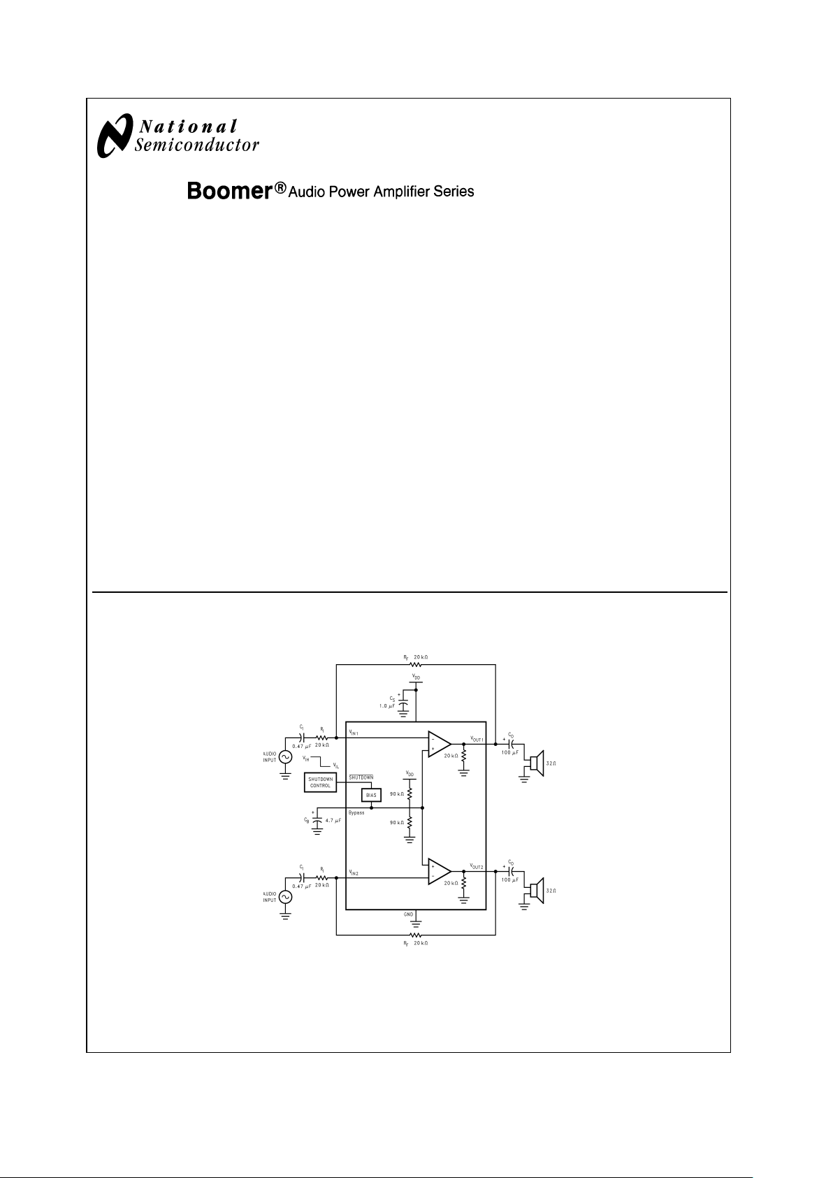
Typical Application
Boomer®is a registered trademark of National Semiconductor Corporation.
20009001
*Refer to the Application Information Section for information concerning proper selection of the input and output coupling capacitors.
FIGURE 1. Typical Audio Amplifier Application Circuit
November 2002
LM4809 Dual 105mW Headphone Amplifier with Active-Low Shutdown Mode
© 2002 National Semiconductor Corporation DS200090 www.national.com
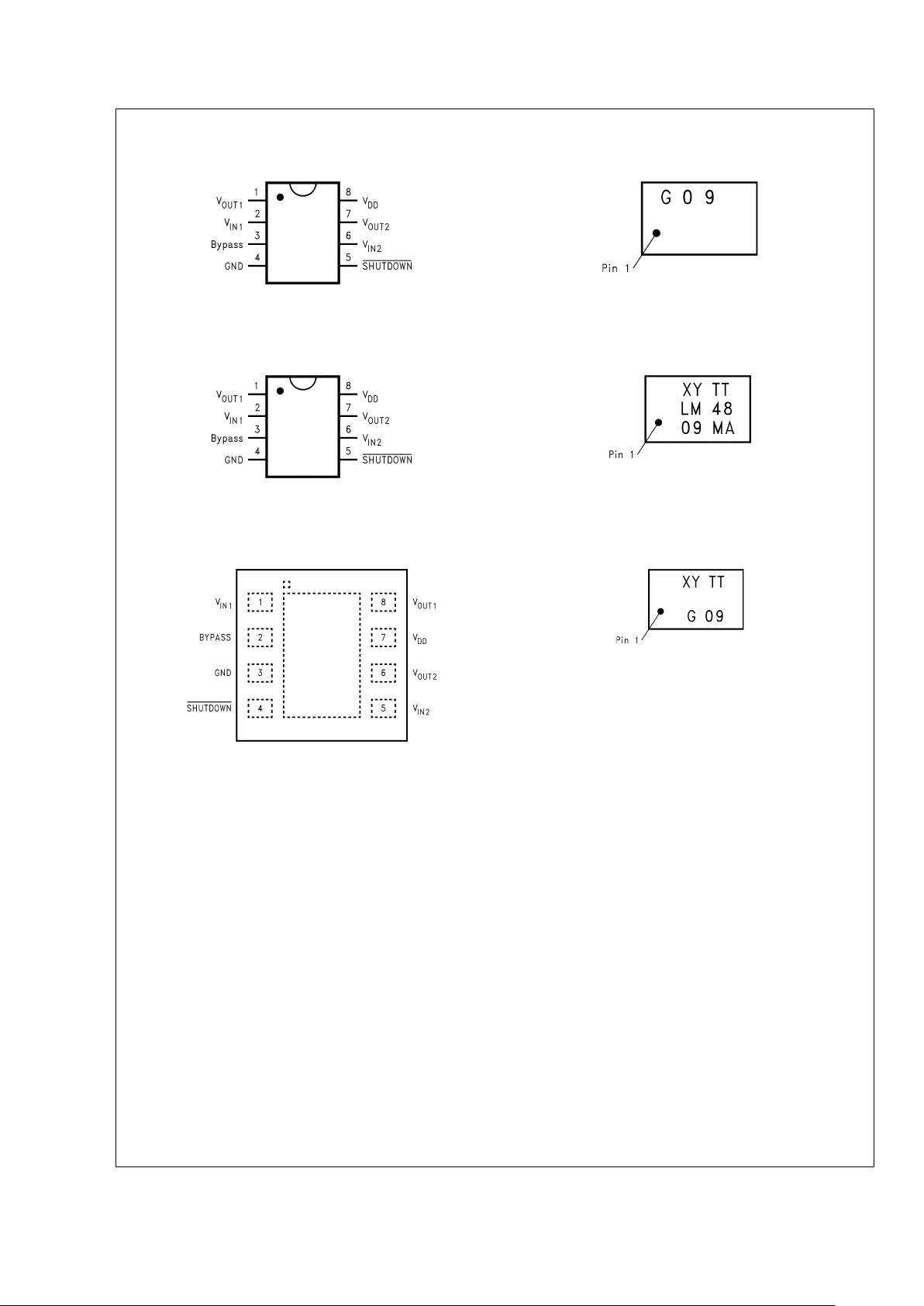
Connection Diagrams
MSOP Package MSOP Marking
20009002
Top View
Order Number LM4809MM
See NS Package Number MUA08A
20009066
SO Package SO Marking
20009002
Top View
Order Number LM4809MA
See NS Package Number M08A
20009067
LLP Package LLP Marking
20009061
Top View
Order Number LM4809LD
See NS Package Number LDA08B
20009068
LM4809
www.national.com 2
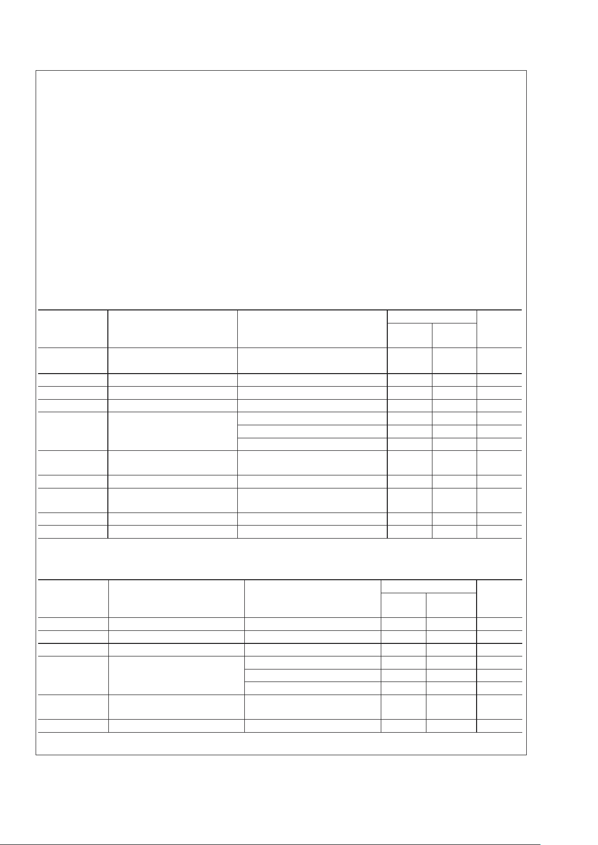
Absolute Maximum Ratings (Note 2)
If Military/Aerospace specified devices are required,
please contact the National Semiconductor Sales Office/
Distributors for availability and specifications.
Supply Voltage 6.0V
Storage Temperature −65˚C to +150˚C
ESD Susceptibility (Note 4) 3.5kV
ESD Machine model (Note 8) 250V
Junction Temperature (T
J
) 150˚C
Soldering Information (Note 1)
Small Outline Package
Vapor Phase (60 sec.) 215˚C
Infrared (15 sec.) 220˚C
Thermal Resistance
θ
JA
(SO) 170˚C/W
θ
JC
(SO) 35˚C/W
θ
JA
(MSOP) 210˚C/W
θ
JC
(MSOP) 56˚C/W
θ
JA
(LLP) 117˚C/W (Note 9)
θ
JA
(LLP) 150˚C/W (Note 10)
θ
JC
(LLP) 15˚C/W
Operating Ratings
Temperature Range
T
MIN
≤ TA≤ T
MAX
−40˚C ≤ TA≤ 85˚C
Supply Voltage (V
CC
) 2.0V ≤ VCC≤ 5.5V
Note 1: See AN-450 “Surface Mounting and their Effects on Product Reliability” for other methods of soldering surface mount devices.
Electrical Characteristics (Notes 2, 3)
The following specifications apply for VDD= 5V unless otherwise specified, limits apply to TA= 25˚C.
Symbol Parameter Conditions LM4809 Units
(Limits)
Typ
(Note 5)
Limit
(Note 7)
V
DD
Supply Voltage 2.0 V (min)
5.5 V (max)
I
DD
Supply Current VIN= 0V, IO= 0A 1.4 3 mA (max)
I
SD
Shutdown Current VIN= 0V, V
SHUTDOWN
= GND 0.4 2 µA(max)
V
OS
Output Offset Voltage VIN= 0V 4.0 50 mV(max)
P
O
Output Power THD+N = 0.1%, f = 1kHz
R
L
=16Ω 105 mW
R
L
=32Ω 70 65 mW (min)
THD+N Total Harmonic Distortion P
O
= 50mW, RL=32Ω
f = 20Hz to 20kHz
0.3 %
Crosstalk Channel Separation RL=32Ω;PO= 70mW 70 dB
PSRR Power Supply Rejection Ratio C
B
= 1.0µF; V
RIPPLE
= 200mVPP,
f = 1kHz; Input terminated into 50Ω
70 dB
V
SDIH
Shutdown Voltage Input High 0.8 x V
DD
V (min)
V
SDIL
Shutdown Voltage Input Low 0.2 x V
DD
V (max)
Electrical Characteristics (Notes 2, 3)
The following specifications apply for VDD= 3.3V unless otherwise specified, limits apply to TA= 25˚C.
Symbol Parameter Conditions LM4809 Units
(Limits)
Typ
(Note 5)
Limit
(Note 7)
I
DD
Supply Current VIN= 0V, IO= 0A 1.1 mA
I
SD
Shutdown Current VIN= 0V, V
SHUTDOWN
= GND 0.4 µA
V
OS
Output Offset Voltage VIN= 0V 4.0 mV
P
O
Output Power THD+N = 0.1%, f = 1kHz
R
L
=16Ω 40 mW
R
L
=32Ω 28 mW
THD+N Total Harmonic Distortion P
O
= 25mW, RL=32Ω
f = 20Hz to 20kHz
0.4 %
Crosstalk Channel Separation R
L
=32Ω;PO= 25mW 70 dB
LM4809
www.national.com3
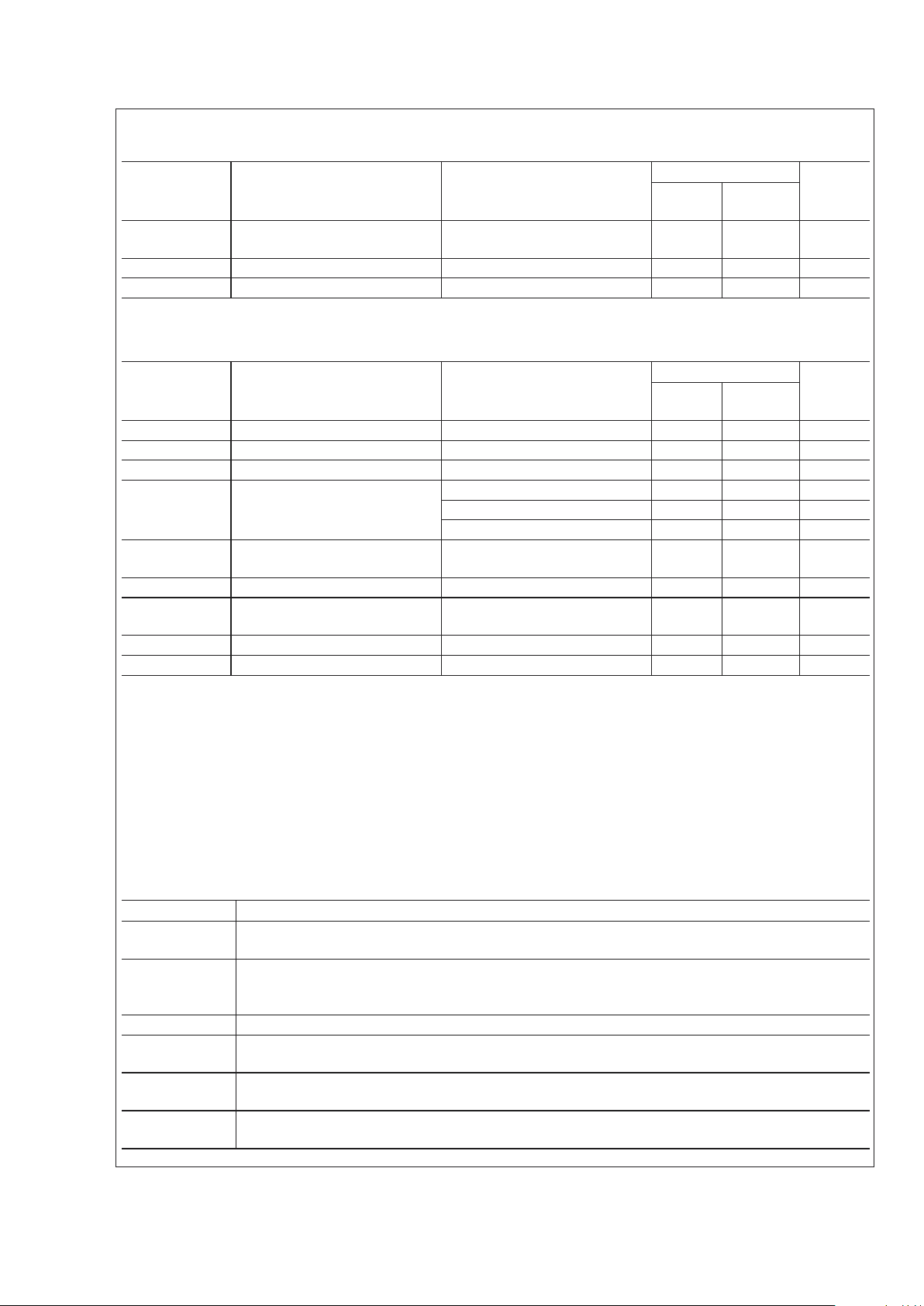
Electrical Characteristics (Notes 2, 3) (Continued)
The following specifications apply for VDD= 3.3V unless otherwise specified, limits apply to TA= 25˚C.
Symbol Parameter Conditions LM4809 Units
(Limits)
Typ
(Note 5)
Limit
(Note 7)
PSRR Power Supply Rejection Ratio C
B
= 1.0µF; V
RIPPLE
= 200mVPP,
f = 1kHz; Input terminated into 50Ω
70 dB
V
SDIH
Shutdown Voltage Input High 0.8 x V
DD
V (min)
V
SDIL
Shutdown Voltage Input Low 0.2 x V
DD
V (max)
Electrical Characteristics (Notes 2, 3)
The following specifications apply for VDD= 2.6V unless otherwise specified, limits apply to TA= 25˚C.
Symbol Parameter Conditions LM4809 Units
(Limits)
Typ
(Note 5)
Limit
(Note 7)
I
DD
Supply Current VIN= 0V, IO= 0A 0.9 mA
I
SD
Shutdown Current VIN= 0V, V
SHUTDOWN
= GND 0.2 µA
V
OS
Output Offset Voltage VIN= 0V 4.0 mV
P
O
Output Power THD+N = 0.1%, f = 1kHz
R
L
=16Ω 20 mW
R
L
=32Ω 16 mW
THD+N Total Harmonic Distortion P
O
= 15mW, RL=32Ω
f = 20Hz to 20kHz
0.6 %
Crosstalk Channel Separation R
L
=32Ω;PO= 15mW 70 dB
PSRR Power Supply Rejection Ratio C
B
= 1.0µF; V
RIPPLE
= 200mVPP,
f = 1kHz; Input terminated into 50Ω
70 dB
V
SDIH
Shutdown Voltage Input High 0.8 x V
DD
V (min)
V
SDIL
Shutdown Voltage Input Low 0.2 x V
DD
V (max)
Note 2: Absolute Maximum Ratings indicate limits beyond which damage to the device may occur.
Note 3: All voltages are measured with respect to the ground pin, unless otherwise specified.
Note 4: Human body model, 100pF discharged through a 1.5kΩ resistor.
Note 5: Typical specifications are specified at +25OC and represent the most likely parametric norm.
Note 6: Tested limits are guaranteed to National’s AOQL (Average Outgoing Quality Level).
Note 7: Datasheet min/max specification limits are guaranteed by design, test, or statistical analysis.
Note 8: Machine Model ESD test is covered by specification EIAJ IC-121-1981. A 200pF cap is charged to the specified voltage, then discharged directly into the
IC with no external series resistor (resistance of discharge path must be under 50Ohms).
Note 9: The given θ
JA
is for an LM4809 packaged in an LDA08B wit the Exposed-Dap soldered to a printed circuit board copper pad with an area equivalent to that
of the Exposed-Dap itself.
Note 10: The given θ
JA
is for an LM4809 packaged in an LDA08B with the Exposed-Dap not soldered to any printed circuit board copper.
External Components Description (Figure 1)
Components Functional Description
1. R
i
The inverting input resistance, along with Rf, set the closed-loop gain. Ri, along with Ci, form a high
pass filter with f
c
= 1/(2πRiCi).
2. C
i
The input coupling capacitor blocks DC voltage at the amplifier’s input terminals. Ci, along with Ri,
create a highpass filter with f
C
= 1/(2πRiCi). Refer to the section, Selecting Proper External
Components, for an explanation of determining the value of C
i
.
3. R
f
The feedback resistance, along with Ri, set closed-loop gain.
4. C
S
This is the supply bypass capacitor. It provides power supply filtering. Refer to the Application
Information section for proper placement and selection of the supply bypass capacitor.
5. C
B
This is the BYPASS pin capacitor. It provides half-supply filtering. Refer to the section, Selecting
Proper External Components, for information concerning proper placement and selection of C
B
.
6. C
O
This is the output coupling capacitor. It blocks the DC voltage at the amplifier’s output and forms a high
pass filter with R
L
at fO= 1/(2πRLCO)
LM4809
www.national.com 4
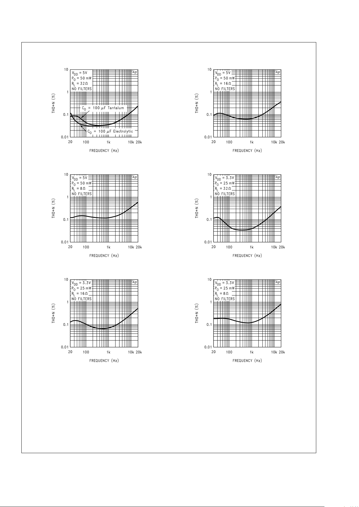
Typical Performance Characteristics
THD+N vs Frequency THD+N vs Frequency
20009003 20009004
THD+N vs Frequency THD+N vs Frequency
20009005 20009006
THD+N vs Frequency THD+N vs Frequency
20009007 20009008
LM4809
www.national.com5
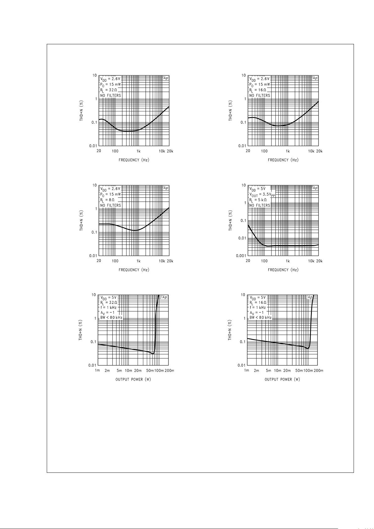
Typical Performance Characteristics (Continued)
THD+N vs Frequency THD+N vs Frequency
20009009 20009010
THD+N vs Frequency THD+N vs Frequency
20009011 20009012
THD+N vs Output Power THD+N vs Output Power
20009013 20009014
LM4809
www.national.com 6
 Loading...