

NSC LM4766TF Datasheet
LM4766 Overture
™
Audio Power Amplifier Series Dual 40W Audio Power
Amplifier with Mute
General Description
The LM4766 is a stereo audio amplifier capable of delivering
typically 40W per channel with the non-isolated "T" package
and 30W per channel with the isolated "TF" package of
continuous average output power into an 8Ω load with less
than 0.1% (THD+N).
The performance of the LM4766, utilizing its Self Peak Instantaneous Temperature (˚Ke) (SPiKe
™
) Protection Circuitry, places it in a class above discrete and hybrid amplifiers by providing an inherently, dynamically protected Safe
Operating Area (SOA). SPiKe Protection means that these
parts are safeguarded at the output against overvoltage,
undervoltage, overloads, including thermal runaway and instantaneous temperature peaks.
Each amplifier within the LM4766 has an independent
smooth transition fade-in/out mute that minimizes output
pops. The IC’s extremely low noise floor at 2µV and its
extremely low THD+N value of 0.06% at the rated power
make the LM4766 optimum for high-end stereo TVs or minicomponent systems.
Key Specifications
n THD+N at 1kHz at 2 x 30W continuous average output
power into 8Ω: 0.1% (max)
n THD+N at 1kHz at continuous average output power of
2 x 30W into 8Ω: 0.009% (typ)
Features
n SPiKe Protection
n Minimal amount of external components necessary
n Quiet fade-in/out mute mode
n Non-Isolated 15-lead TO-220 package
n Wide Supply Range 20V - 78V
Applications
n High-end stereo TVs
n Component stereo
n Compact stereo
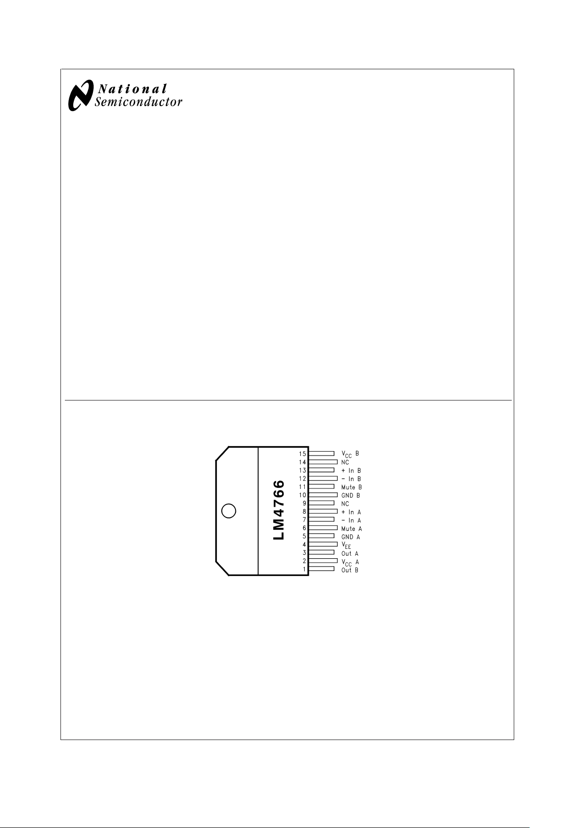
Connection Diagram
Plastic Package
10092802
Top View
Non-Isolated TO-220 Package
Order Number LM4766T
See NS Package Number TA15A
Isolated TO-220 Package
Order Number LM4766TF
See NS Package Number TF15B
SPiKe™Protection and Overture™are trademarks of National Semiconductor Corporation.
July 2003
LM4766 Overture
™
Audio Power Amplifier Series
Dual 40W Audio Power Amplifier with Mute
© 2003 National Semiconductor Corporation DS100928 www.national.com
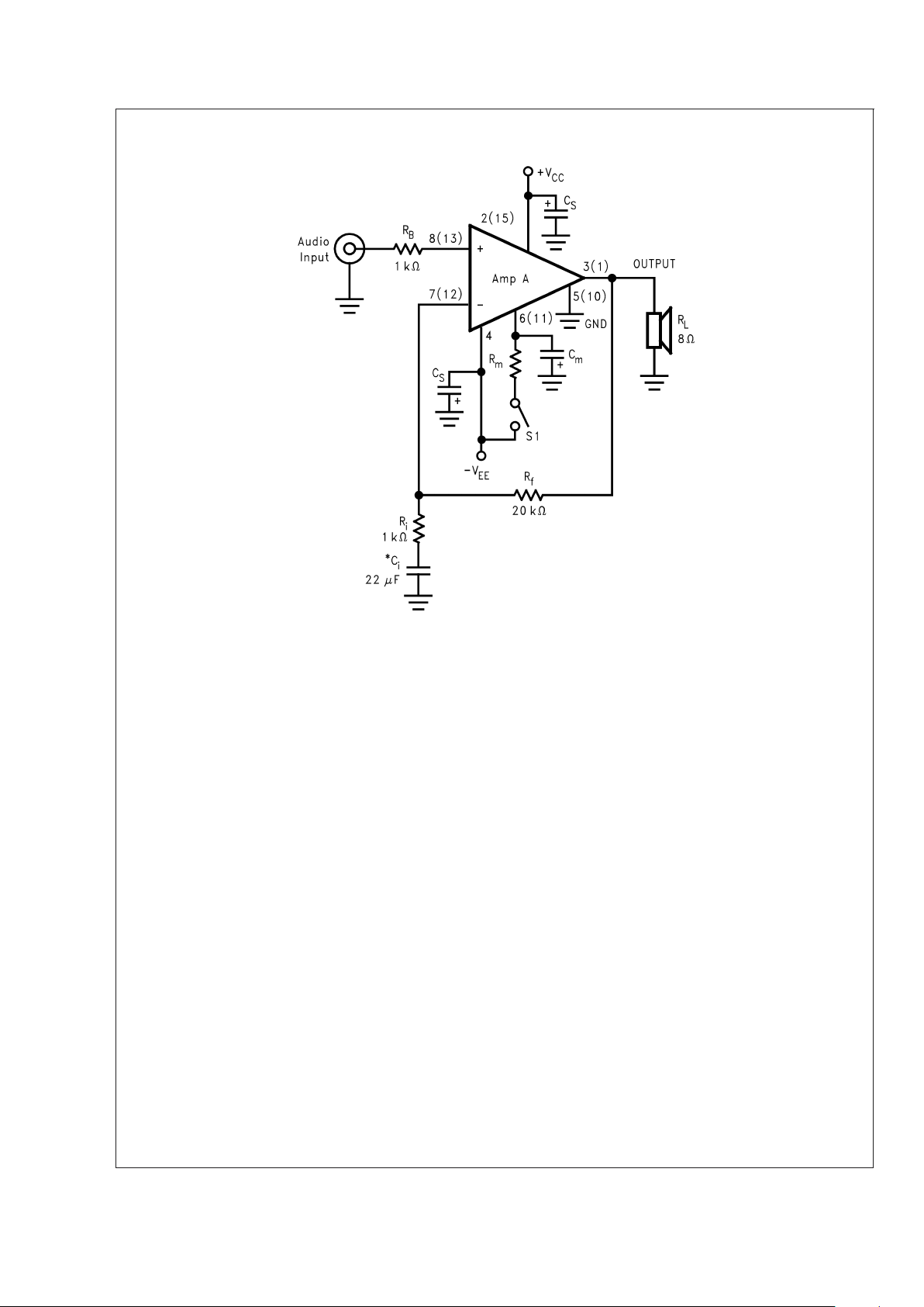
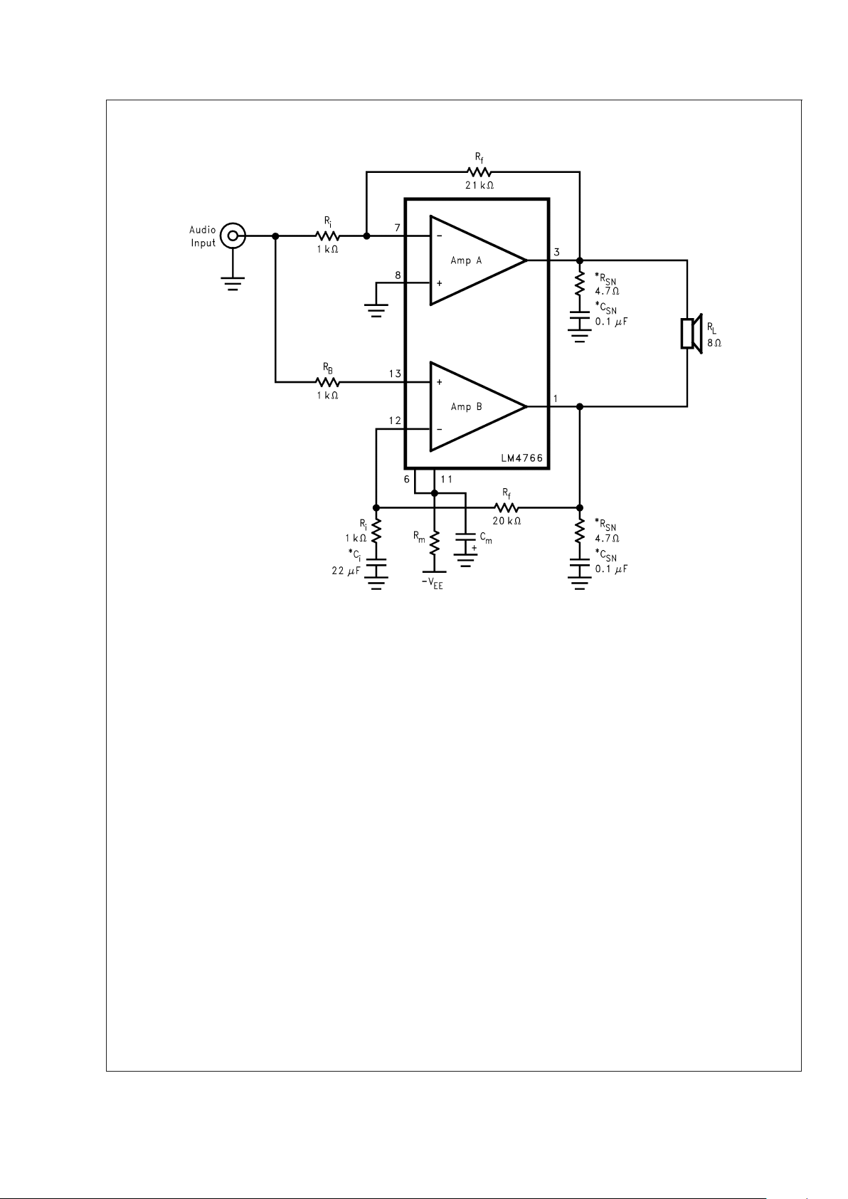
Typical Application
Note: Numbers in parentheses represent pinout for amplifier B.
*
Optional component dependent upon specific design requirements.
10092801
FIGURE 1. Typical Audio Amplifier Application Circuit
LM4766
www.national.com 2

Absolute Maximum Ratings (Notes 4,
5)
If Military/Aerospace specified devices are required,
please contact the National Semiconductor Sales Office/
Distributors for availability and specifications.
Supply Voltage |V
CC
|+|VEE|
(No Input) 78V
Supply Voltage |V
CC
|+|VEE|
(with Input) 74V
Common Mode Input Voltage (V
CC
or VEE) and
|V
CC
|+|VEE| ≤
60V
Differential Input Voltage 60V
Output Current Internally Limited
Power Dissipation (Note 6) 62.5W
ESD Susceptability (Note 7) 3000V
Junction Temperature (Note 8) 150˚C
Thermal Resistance
Non-Isolated T-Package
θ
JC
1˚C/W
Isolated TF-Package
θ
JC
2˚C/W
Soldering Information
T and TF Packages 260˚C
Storage Temperature −40˚C to +150˚C
Operating Ratings (Notes 4, 5)
Temperature Range
T
MIN
≤ TA≤ T
MAX
−20˚C ≤ TA≤
+85˚C
Supply Voltage |V
CC
|+|VEE| (Note
1) 20V to 60V
Electrical Characteristics (Notes 4, 5)
The following specifications apply for VCC= +30V, VEE= −30V, I
MUTE
= −0.5mA with RL=8Ω unless otherwise specified. Lim-
its apply for T
A
= 25˚C.
Symbol Parameter Conditions LM4766 Units
(Limits)
Typical Limit
(Note 9) (Note 10)
|V
CC
| + Power Supply Voltage GND − VEE≥ 9V 18 20 V (min)
|V
EE
| (Note 11) 60 V (max)
P
O
Output Power T Package, VCC=±30V,
THD+N = 0.1% (max),
f = 1kHz, f = 20kHz
40 30 W/ch (min)
TF Package, V
CC
=±26V(Note 13),
THD+N = 0.1% (max),
30 25 W/ch (min)
(Notes 3, 13) (Continuous Average) f = 1kHz, f = 20kHz
THD+N Total Harmonic Distortion
Plus Noise
T Package
30W/ch, R
L
=8Ω, 20Hz ≤ f ≤ 20kHz,
A
V
= 26dB
0.06 %
TF Package
25W/ch, R
L
=8Ω, 20Hz ≤ f ≤ 20kHz,
A
V
= 26dB
0.06 %
X
talk
Channel Separation f = 1kHz, VO= 10.9Vrms 60 dB
SR
(Note 3)
Slew Rate V
IN
= 1.2Vrms, t
rise
= 2ns 9 5 V/µs (min)
I
total
Total Quiescent Power Both Amplifiers VCM= 0V, 48 100 mA (max)
(Note 2) Supply Current V
O
= 0V, IO= 0mA
V
OS
(Note 2)
Input Offset Voltage V
CM
= 0V, IO= 0mA 1 10 mV (max)
I
B
Input Bias Current VCM= 0V, IO= 0mA 0.2 1 µA (max)
I
OS
Input Offset Current VCM= 0V, IO= 0mA 0.01 0.2 µA (max)
I
O
Output Current Limit |VCC|=|VEE| = 10V, tON= 10ms, 4 3 Apk (min)
V
O
=0V
V
OD
Output Dropout Voltage |VCC–VO|, VCC= 20V, IO= +100mA 1.5 4 V (max)
(Note 2) (Note 12) |V
O–VEE
|, VEE= −20V, IO= −100mA 2.5 4 V (max)
LM4766
www.national.com3
Electrical Characteristics (Notes 4, 5) (Continued)
The following specifications apply for VCC= +30V, VEE= −30V, I
MUTE
= −0.5mA with RL=8Ω unless otherwise specified. Lim-
its apply for T
A
= 25˚C.
Symbol Parameter Conditions LM4766 Units
(Limits)
Typical Limit
(Note 9) (Note 10)
PSRR Power Supply Rejection Ratio V
CC
= 30V to 10V, VEE= −30V, 125 85 dB (min)
(Note 2) V
CM
= 0V, IO= 0mA
V
CC
= 30V, VEE= −30V to −10V 110 85 dB (min)
V
CM
= 0V, IO= 0mA
CMRR Common Mode Rejection Ratio V
CC
= 50V to 10V, VEE= −10V to −50V, 110 75 dB (min)
(Note 2) V
CM
= 20V to −20V, IO= 0mA
A
VOL
(Note 2)
Open Loop Voltage Gain R
L
=2kΩ, ∆ VO= 40V 115 80 dB (min)
GBWP Gain Bandwidth Product f
O
= 100kHz, VIN= 50mVrms 8 2 MHz (min)
e
IN
Input Noise IHF — A Weighting Filter 2.0 8 µV (max)
(Note 3) R
IN
= 600Ω (Input Referred)
SNR Signal-to-Noise Ratio P
O
= 1W, A—Weighted, 98 dB
Measured at 1kHz, R
S
=25Ω
P
O
= 25W, A—Weighted 112 dB
Measured at 1kHz, R
S
=25Ω
A
M
Mute Attenuation Pin 6,11 at 2.5V 115 80 dB (min)
Note 1: Operation is guaranteed up to 60V, however, distortion may be introduced from SPiKe Protection Circuitry if proper thermal considerations are not taken
into account. Refer to the Application Information section for a complete explanation.
Note 2: DC Electrical Test; Refer to Test Circuit
#
1.
Note 3: AC Electrical Test; Refer to Test Circuit
#
2.
Note 4: All voltages are measured with respect to the GND pins (5, 10), unless otherwise specified.
Note 5: Absolute Maximum Ratings indicate limits beyond which damage to the device may occur. Operating Ratings indicate conditions for which the device is
functional, but do not guarantee specific performance limits. Electrical Characteristics state DC and AC electrical specifications under particular test conditions which
guarantee specific performance limits. This assumes that the device is within the Operating Ratings. Specifications are not guaranteed for parameters where no limit
is given, however, the typical value is a good indication of device performance.
Note 6: For operating at case temperatures above 25˚C, the device must be derated based on a 150˚C maximum junction temperature and a thermal resistance
of θ
JC
= 1˚C/W (junction to case) for the T package. Refer to the section Determining the Correct Heat Sink in the Application Information section.
Note 7: Human body model, 100pF discharged through a 1.5kΩ resistor.
Note 8: The operating junction temperature maximum is 150˚C, however, the instantaneous Safe Operating Area temperature is 250˚C.
Note 9: Typicals are measured at 25˚C and represent the parametric norm.
Note 10: Limits are guarantees that all parts are tested in production to meet the stated values.
Note 11: V
EE
must have at least −9V at its pin with reference to ground in order for the under-voltage protection circuitry to be disabled. In addition, the voltage
differential between V
CC
and VEEmust be greater than 14V.
Note 12: The output dropout voltage, V
OD
, is the supply voltage minus the clipping voltage. Refer to the Clipping Voltage vs. Supply Voltage graph in the Typical
Performance Characteristics section.
Note 13: When using the isolated package (TF), the θ
JC
is 2˚C/W verses 1˚C/W for the non-isolated package (T). This increased thermal resistance from junction
to case requires a lower supply voltage for decreased power dissipation within the package. Voltages higher than
±
26V maybe used but will require a heat sink with
less than 1˚C/W thermal resistance to avoid activating thermal shutdown during normal operation.
LM4766
www.national.com 4
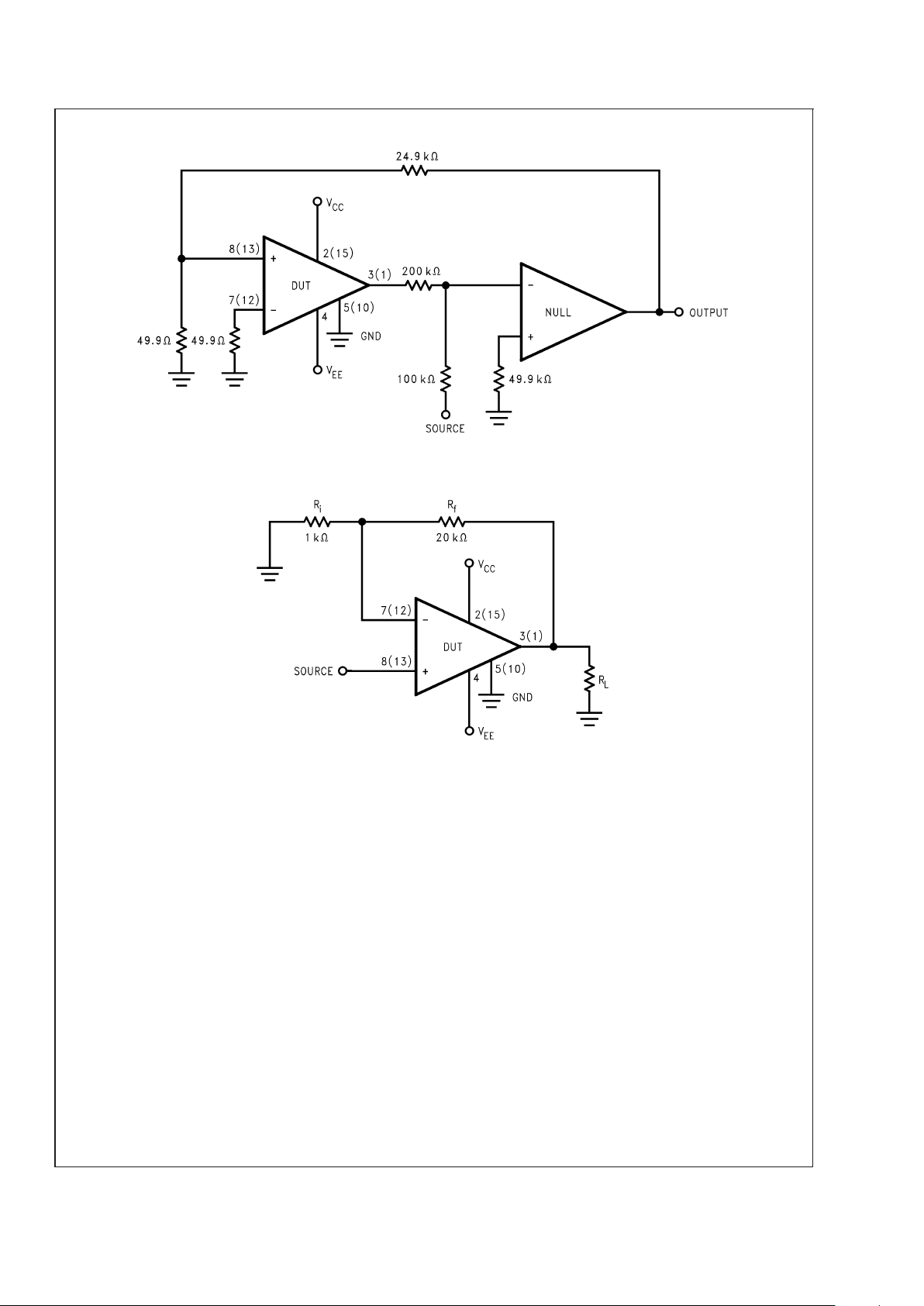
Test Circuit#1 (Note 2) (DC Electrical Test Circuit)
10092803
Test Circuit#2 (Note 3) (AC Electrical Test Circuit)
10092804
LM4766
www.national.com5
Bridged Amplifier Application Circuit
10092805
FIGURE 2. Bridged Amplifier Application Circuit
LM4766
www.national.com 6
 Loading...