

LM4755
Stereo 11W Audio Power Amplifier with Mute
n P
at 10%THD@1 kHz into 8Ω bridged TO-263 pkg.
General Description
The LM4755 is a stereo audio amplifier capable of delivering
11W per channel of continuous average output power to a
4Ω load or7Wperchannel into 8Ω using a single 24V supply
at 10%THD+N. The internal mute circuit and pre-set gain resistors provide for a very economical design solution.
Output power specifications at both 20V and 24V supplies
and low external component count offer high value to consumer electronic manufacturers for stereo TV and compact
stereo applications. The LM4755 is specifically designed for
single supply operation.
Key Specifications
n Output power at 10%THD with 1 kHz into 4Ω at VCC=
24V 11W(typ)
n Output power at 10%THD with 1 kHz into 8Ω at V
24V 7W(typ)
n Closed loop gain 34 dB(typ)
n P
at 10%THD@1 kHz into 4Ω single-ended TO-263
O
pkg. at V
=
12V 2.5W(typ)
CC
=
CC
O
=
at V
12V 5W(typ)
CC
Features
n Drives 4Ω and 8Ω loads
n Integrated mute function
n Internal Gain Resistors
n Minimal external components needed
n Single supply operation
n Internal current limiting and thermal protection
n Compact 9-lead TO-220 package
Applications
n Stereos TVs
n Compact stereos
n Mini component stereos
LM4755 Stereo 11W Audio Power Amplifier with Mute
February 1999
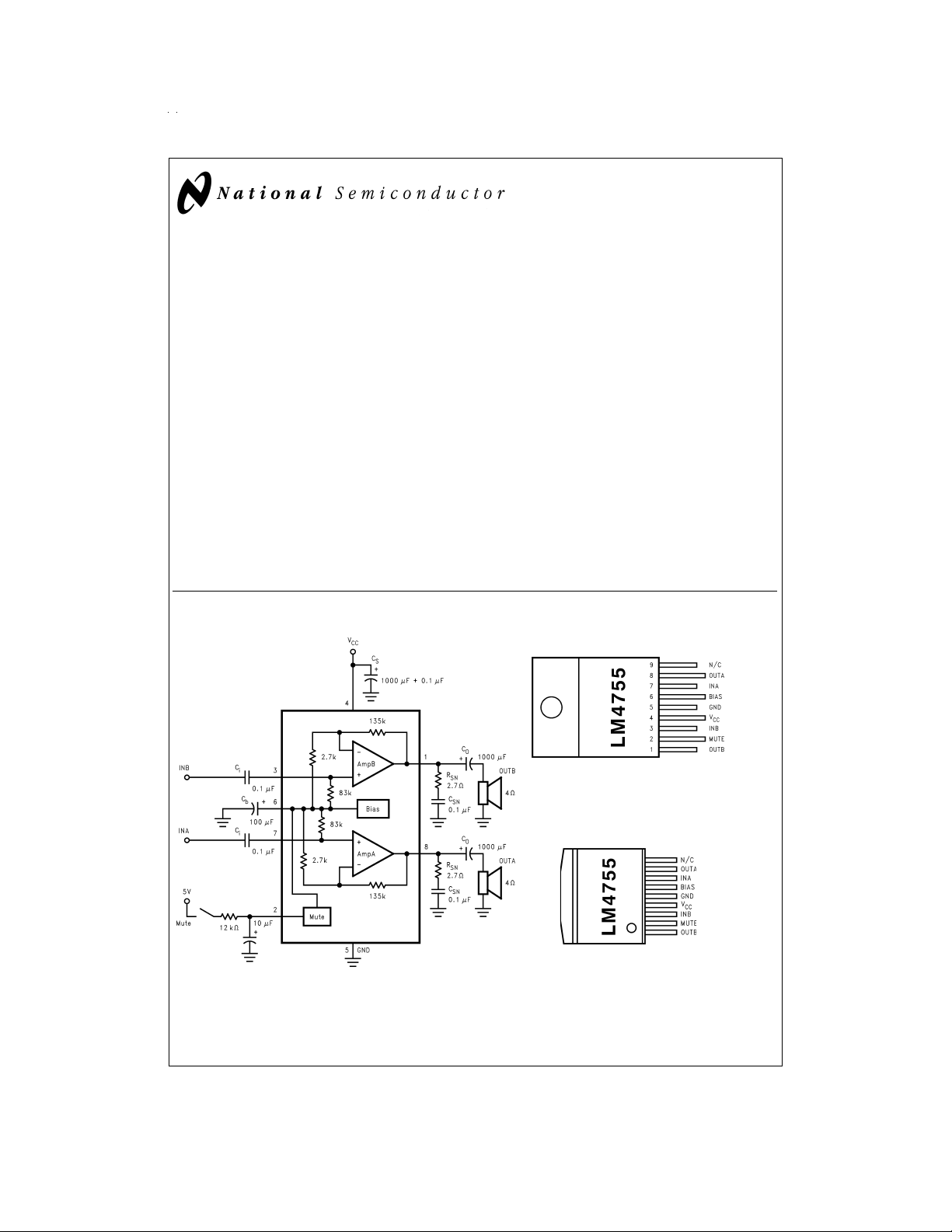
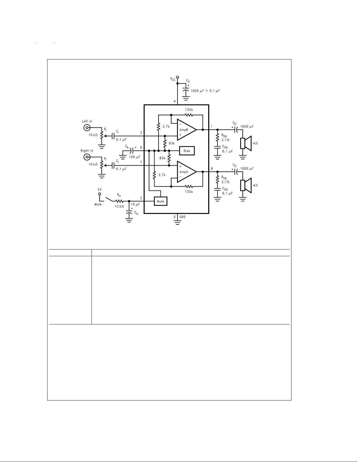
Typical Application Connection Diagrams
Plastic Package
Package Description
Top View
Order Number LM4755T
Package Number TA09A
DS100059-1
FIGURE 1. Typical Audio Amplifier Application Circuit
Top View
Order Number LM4755TS
Package Number TS9A
DS100059-2
DS100059-36
© 1999 National Semiconductor Corporation DS100059 www.national.com
Absolute Maximum Ratings (Note 2)
If Military/Aerospace specified devices are required,
T Package (10 seconds) 250˚C
Storage Temperature −40˚C to 150˚C
please contact the National Semiconductor Sales Office/
Distributors for availability and specifications.
Supply Voltage 40V
Input Voltage
±
0.7V
Output Current Internally Limited
Power Dissipation (Note 3) 62.5W
ESD Susceptability (Note 4) 2 kV
Junction Temperature 150˚C
Operating Ratings
Temperature Range
T
≤ TA≤ T
MIN
MAX
Supply Voltage 9V to 32V
θ
JC
θ
JA
−40˚C ≤ TA≤ +85˚C
2˚C/W
76˚C/W
Soldering Information
Electrical Characteristics
The following specifications apply to each channel with VCC= 24V, TA= 25˚C unless otherwise specified.
Symbol Parameter Conditions
I
TOTAL
Total Quiescent Power
Supply Current
Mute Off 10 15 mA(max)
Typical
(Note 5)
Limit
7 mA(min)
Mute On 7 mA
LM4755
P
O
THD Total Harmonic Distortion f = 1 kHz, P
V
OSW
X
TALK
Output Power (Continuous
Average per Channel)
f = 1 kHz, THD+N = 10%,RL=8Ω 7W
f = 1 kHz, THD+N = 10%,R
V
= 20V, RL=8Ω 4W
S
V
= 20V, RL=4Ω 7W
S
f = 1 kHz, THD+N = 10%,R
= 12V, TO-263 Pkg.
V
S
= 1 W/ch, RL=8Ω 0.08
O
=4Ω 11 10 W(min)
L
=4Ω
L
2.5 W
Output Swing PO= 10W, RL=8Ω 15 V
P
= 10W, RL=4Ω 14 V
O
Channel Separation See Apps. Circuit 55 dB
f = 1 kHz, V
= 4 Vrms
O
PSRR Power Supply Rejection Ratio See Apps. Circuit 50 dB
f = 120 Hz, V
V
ODV
Differential DC Output Offset
Voltage
VIN= 0V 0.09 0.4 V(max)
= 1 mVrms
O
SR Slew Rate 2 V/µs
R
IN
PBW Power Bandwidth 3 dB BW at P
A
VCL
e
IN
I
O
Mute Pin
V
IL
V
IH
A
M
Note 1: All voltages are measured with respect to the GND pin (5), unless otherwse specified.
Note 2: Absolute Maximum Ratings indicate limits beyond which damage to the device may occur.Operating Ratings indicate conditions for which the device is func-
tional, but do not guarantee specific performance limits. Electrical Characteristics state DC and AC electrical specifications under particular test conditions which guarantee specific performance limits. This assumes that the device is within the Operating Ratings. Specifications are not guaranteed for parameters where no limit is
given, however, the typical value is a good indication of device performance.
Note 3: For operating at case temperatures above 25˚C, the device must be derated based on a 150˚C maximum junction temperature and a thermal resistance of
= 2˚C/W (junction to case). Refer to the section Determining the Maximum Power Dissipation in the Application Information section for more information.
θ
JC
Note 4: Human body model, 100 pF discharged through a 1.5 kΩ resistor.
Input Impedance 83 kΩ
= 2.5W, RL=8Ω 65 kHz
Closed Loop Gain
RL=8Ω 34 33 dB(min)
(Internally Set)
Noise IHF-A Weighting Filter, RL=8Ω
O
35 dB(max)
0.2 mVrms
Output Referred
Output Short Circuit Limit VIN= 0.5V, RL=2Ω 2 A(min)
Mute Low Input Voltage Not in Mute Mode 0.8 V(max)
Mute High Input Voltage In Mute Mode 2.0 2.5 V(min)
Mute Attenuation V
= 5.0V 80 dB
MUTE
Units
(Limits)
%
www.national.com 2
Electrical Characteristics (Continued)
Note 5: Typicals are measured at 25˚C and represent the parametric norm.
Note 6: Limits are guaranteed that all parts are tested in production to meet the stated values.
Note 7: The TO-263 Package is not recommended for V
>
16V due to impractical heatsinking limitations.
S
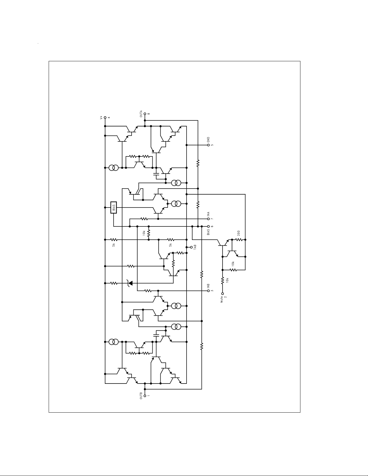
Equivalent Schematic
DS100059-3
www.national.com3
Test Circuit
FIGURE 2. Test Circuit
www.national.com 4
DS100059-4
System Application Circuit
FIGURE 3. Circuit for External Components Description
External Components Description
DS100059-5
Components Function Description
1, 2 C
3, 4 R
5, 6 C
7C
8, 9 C
10, 11 C
12, 13 R
14 R
15 C
Provides power supply filtering and bypassing.
S
Works with CSNto stabilize the output stage from high frequency oscillations.
SN
Works with RSNto stabilize the output stage from high frequency oscillations.
SN
Provides filtering for the internally generated half-supply bias generator.
b
Input AC coupling capacitor which blocks DC voltage at the amplifier’s input terminals. Also creates a
i
high pass filter with fc=1/(2
Output AC coupling capacitor which blocks DC voltage at the amplifier’s output terminal. Creates a high
o
pass filter with fc=1/(2
Voltage control - limits the voltage level allowed to the amplifier’s input terminals.
i
Works with Cmto provide mute function timing.
m
Works with Rmto provide mute function timing.
m
•π•
Rin•Cin).
•π•
Rout•Cout).
www.national.com5
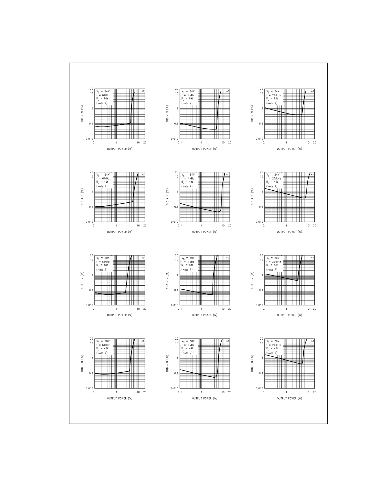
Typical Performance Characteristics(Note 5)
THD+N vs Output Power
THD+N vs Output Power
THD+N vs Output Power
DS100059-12
DS100059-6
THD+N vs Output Power
THD+N vs Output Power
THD+N vs Output Power
DS100059-13
DS100059-7
THD+N vs Output Power
DS100059-14
THD+N vs Output Power
DS100059-8
THD+N vs Output Power
DS100059-15
THD+N vs Output Power
DS100059-9
THD+N vs Output Power
www.national.com 6
DS100059-16
DS100059-10
DS100059-17
THD+N vs Output Power
DS100059-11
 Loading...