

NSC LM4663MT Datasheet
January 2000
LM4663
2 Watt Stereo Class D Audio Power Amplifier with Stereo
Headphone Amplifier
LM4663 2 Watt Stereo Class D Audio Power Amplifier with Stereo Headphone Amplifier
General Description
The LM4663 is a fully integrated single supply, high efficiency Class D audio power amplifier solution. The LM4663
utilizes a continuous time delta-sigma modulation technique
that lowers output noise and THD when compared to conventional pulse width modulators.
The LM4663also features a stereo headphone amplifier that
delivers 80mW into a 32Ω headset with lessthan 0.5%THD.
The LM4663 has two stereo inputs that can be selected to
drive either the headphone amplifier or the Class D amplifier.
All amplifiers are protected with thermal shutdown.
In standby mode, the LM4663 draws an extremely low 2µA
supply current. With a 4Ω load, the IC’s efficiency for a
250mW power level is 69%, reaching 83%at a power level
of 2W. The IC features click and pop reduction circuitry that
minimizes audible popping during device turn-on and
turn-off. The LM4663 is available in a 24-lead TSSOP package, ideal for portable and desktop computer applications.
Key Specifications
n POat THD+N=1
n THD+N at 1kHz at 1 Watt into 4Ω (Power
Amp) 0.2%(typ)
%
2.1W (typ)
n Efficiency at 2 Watt into 4Ω 83%(typ)
n Efficiency at 250mW into 4Ω 69%(typ)
n Total quiescent power supply current 22mA (typ)
n Total shutdown power supply current 2µA (typ)
n THD+N 1kHz, 20mW, 32Ω (Headphone) 0.15%(typ)
n Single supply range 4.5V to 5.5V
Features
n Delta-sigma modulator.
n Two stereo input selector.
n “Click and pop” suppression circuitry.
n Micropower shutdown mode.
n 24 lead TSSOP package (No heatsink required).
n Stereo headphone amplifier.
Applications
n Portable computers
n Desktop computers
n Multimedia Monitors
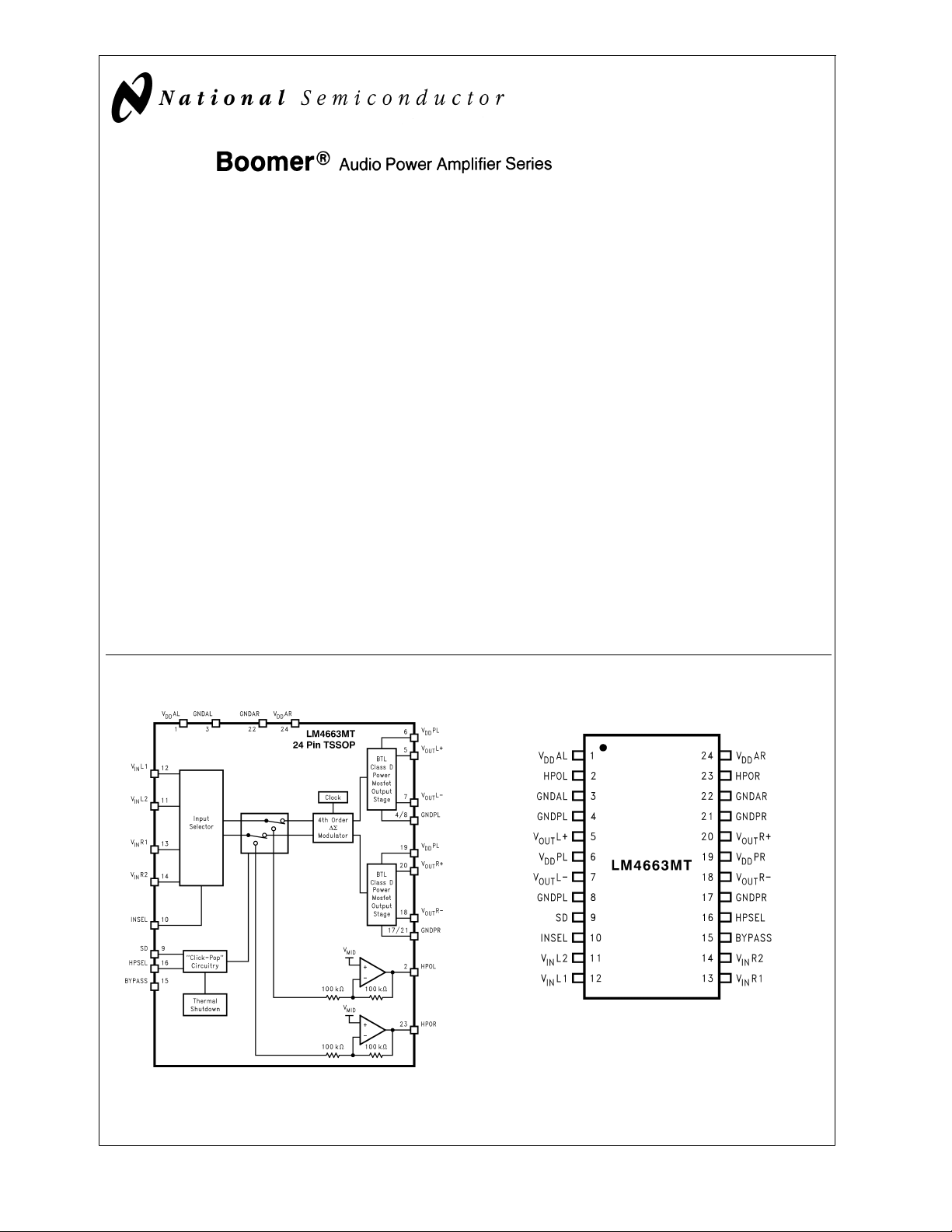
Block Diagram Connection Diagram
TSSOP Package
DS101269-2
Top View
Order Number LM4663MT
See NS Package Number MTC24
DS101269-1
BOOMER™is a trademark of National Semiconductor Corporation.
© 2000 National Semiconductor Corporation DS101269 www.national.com
(TSSOP Package)
Absolute Maximum Ratings (Note 2)
If Military/Aerospace specified devices are required,
LM4663
please contact the National Semiconductor Sales Office/
Distributors for availability and specifications.
Supply Voltage 6.0V
Input Voltage −0.3V to V
DD
+0.3V
Power Dissipation (Note 3) Internally Limited
Load Resistance 2.5Ω, min
ESD Susceptibility(Note 4) 2000V
Pins 5,7,18,20 600V
ESD Susceptibility (Note 5) 200V
Pins 5,7,18,20 50V
Junction Temperature (Note 6) 150˚C
Storage Temperature −65˚C ≤ T
≤ 150˚C
A
Electrical Characteristics (Notes 1, 2, 7)
The following specifications apply for V
Limits apply for T
= 25˚C.
A
=
DD
Symbol Parameter Conditions
V
S
I
S
I
S
I
SD
R
IN
V
IH
V
IL
V
IH
V
IL
Operating Supply Voltage
Range
Quiescent Power Supply
Current, Class D Mode
Quiescent Power Supply
Current, Headphone Mode
Quiescent Power Supply
Current, Shutdown Mode
Input Resistance in Both Modes 20 kΩ
Minimum High Level Input
Voltage
Maximum Low Level Input
Voltage
Minimum High Level Input
Voltage
Maximum Low Level Input
Voltage
Power Amplifiers
P
R Output Power, Per Channel THD+N ≤ 1%,f
O
P
D1
P
D2
P
D3
E
FF1
E
FF2
E
FF3
Power Dissipation P
Power Dissipation P
Power Dissipation P
Efficiency P
Efficiency
Efficiency P
THD+N Harmonic Distortion + Noise P
V
NOISE
PSRR
A
V
A
L−AVR Stereo Gain Tracking 1kHz, V
V
Output Noise Voltage, RMS.
A−Weighted
Power Supply Rejection Ratio
(Referred to Input)
Voltage Gain 1kHz, V
=
5V, R
4Ω, LC filter values as shown in Figure 1, unless otherwise specified.
L
=
V
0V
IN
RMS,VHPSEL
=
V
0V
IN
RMS,VHPSEL
=
V
5V 2 µA
SD
Shutdown Pin & Input Select
Pin
Shutdown Pin & Input Select
Pin
Headphone Select Pin 4.5 V
Headphone Select Pin 0.5 V
=
2W/Chan, f
O
=
1W/Chan, f
O
=
.25W/Chan, f
O
=
2W/Chan, f
O
=
1W/Chan, R
P
O
1kHz
=
.25W/Chan, f
O
=
1W/Chan, f
O
R
SOURCE
=
BW=8Hz to 22kHz
200mV, 1kHz, V
=
IN
=
IN
Soldering Information
TSSOP Package
Vapor Phase (60 sec.) 215˚C
Infrared (15 sec.) 220˚C
See AN-450 “Surface Mounting and their Effects on
Product Reliability” for other methods of soldering surface
mount devices.
Operating Ratings(Notes 1, 2)
Temperature Range
T
≤ TA≤ T
MIN
MAX
Supply Voltage 4.5V ≤ V
Thermal Resistance (TSSOP Package)
θ
JA
θ
JC
LM4663
Typical Max Min
5 5.5 4.5 V
=
0V 22 35 mA
=
V
S
510 mA
0.5 V
=
1kHz 2.1 W
IN
=
1kHz 0.82 W
IN
=
1kHz 0.49 W
IN
=
1kHz 0.23 W
IN
=
1kHz 83
IN
L
IN
IN
50Ω,C
IN
=
IN
100mV, R
100mV, R
=
=
=
044
=
8Ω,f
IN
85 80
1kHz 69
1kHz 0.2
=
1µF,
=
4Ω 13 dB
L
=
4Ω 0.1 dB
L
200 µV
−40˚C ≤ TA≤ +85˚C
≤ 5.5V
DD
80˚C/W
20˚C/W
Units
4.5 V
%
%
%
%
dB
www.national.com 2
Electrical Characteristics (Notes 1, 2, 7) (Continued)
The following specifications apply for V
Limits apply for T
= 25˚C.
A
=
DD
Symbol Parameter Conditions
Headphone Amplifiers
P
O
Power Out Per Channel THD+N ≤ 1%,R
THD+N Distortion + Noise
V
NOISE
PSRR
A
V
A
L−AVR Stereo Gain Tracking 1kHz, V
V
Note 1: All voltages are measured with respect to the ground pin, unless otherwise specified.
Note 2:
functional, but do not guarantee specific performance limits.
guarantee specific performance limits. This assumes that the device iswithin the Operating Ratings. Specifications are not guaranteed for parameters where no limit
is given, however, the typical value is a good indication of device performance.
Note 3: For operating at case temperatures above 25˚C, the device must be derated based on a 150˚C maximum junction temperature and a thermal resistance of
= 80˚C/W (junction to ambient).
θ
JA
Note 4: Human body model, 100 pF discharged through a 1.5 kΩ resistor.
Note 5: Machine Model 220pF−240pF discharged through all pins.
Note 6: The operating junction temperature maximum is 150˚C.
Note 7: Limits are guaranteed to National’s AOQL (Average Outgoing Quality Level).
Output Noise Voltage, RMS
Power Supply Rejection Ratio
(Referred to Input)
Voltage Gain 1kHz, V
“Absolute Maximum Ratings”
indicate limits beyond which damage to the device may occur.
=
5V, R
4Ω, LC filter values as shown in Figure 1, unless otherwise specified.
L
1kHz
=
P
20mW, R
O
1kHz
=
50Ω,C
R
IN
IN
8Hz to 22kHz
200mV, 1kHz, V
32Ω
=
100mV, R
IN
=
100mV, R
IN
“Electrical Characteristics”
LM4663
Typical Max Min
=
32Ω,f
L
=
32Ω,f
L
=
1µF, BW
=
0, R
IN
state DC andACelectricalspecificationsunderparticulartestconditionswhich
=
IN
=
IN
=
=
L
=
32Ω 5.5 dB
L
=
32Ω 0.1 dB
L
80 60
0.15
30 µV
44 dB
“Operating Ratings”
indicate conditions for which the device is
Units
mW
LM4663
%
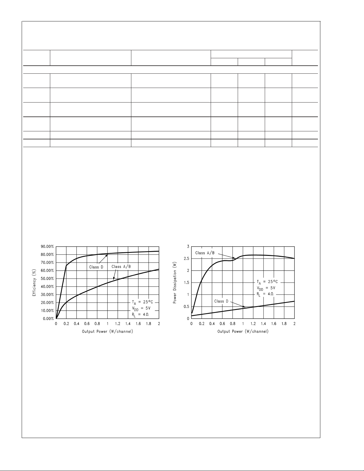
Typical Performace Characteristics
Efficiency vs Output Power
DS101269-10
Power Dissipation vs Output Power
DS101269-11
www.national.com3
 Loading...