

NSC LM4652TF, LM4651N, LM4652TA Datasheet
August 2000
LM4651 & LM4652 Overture
LM4651 & LM4652
Overture
™
Audio Power Amplifier
170W Class D Audio Power Amplifier Solution
General Description
The IC combination of the LM4651 driver and the LM4652
power MOSFET provides a high efficiency, Class D subwoofer amplifier solution.
The LM4651 is a fully integrated conventional pulse width
modulator driver IC. The IC contains short circuit, under
voltage, over modulation, and thermal shut down protection
circuitry. It contains a standby function, which shuts down
the pulse width modulation and minimizes supply current.
The LM4652 is a fully integrated H-bridge power MOSFET
IC in a TO-220 power package. Together, these two IC’s
form a simple, compact high power audio amplifier solution
complete with protection normally seen only in Class AB
amplifiers. Few external components and minimal traces
between the IC’s keep the PCB area small and aids in EMI
control.
The near rail-to-rail switching amplifier substantially increases the efficiencycompared to Class AB amplifiers. This
high efficiency solution significantly reduces the heat sink
size compared to a Class AB IC of the same power level.
This two-chip solution is optimum for powered subwoofers
and self powered speakers.
Key Specifications
n Output power into 4Ω with<10% THD. 170W (Typ)
n THD at 10W, 4Ω, 10 − 500Hz.
n Maximum efficiency at 125W 85% (Typ)
n Standby attenuation.
Features
n Conventional pulse width modulation.
n Externally controllable switching frequency.
n 50kHZ to 200kHz switching frequency range.
n Integrated error amp and feedback amp.
n Turn−on soft start and under voltage lockout.
n Over modulation protection (soft clipping).
n Short circuit current limiting and thermal shutdown
protection.
n 15 Lead TO−220 isolated package.
n Self checking protection diagnostic.
Applications
n Powered subwoofers for home theater and PC’s
n Car booster amplifier
n Self-powered speakers
<
0.3% THD (Typ)
>
100dB (Min)
™
170W Class D Audio Power Amplifier Solution
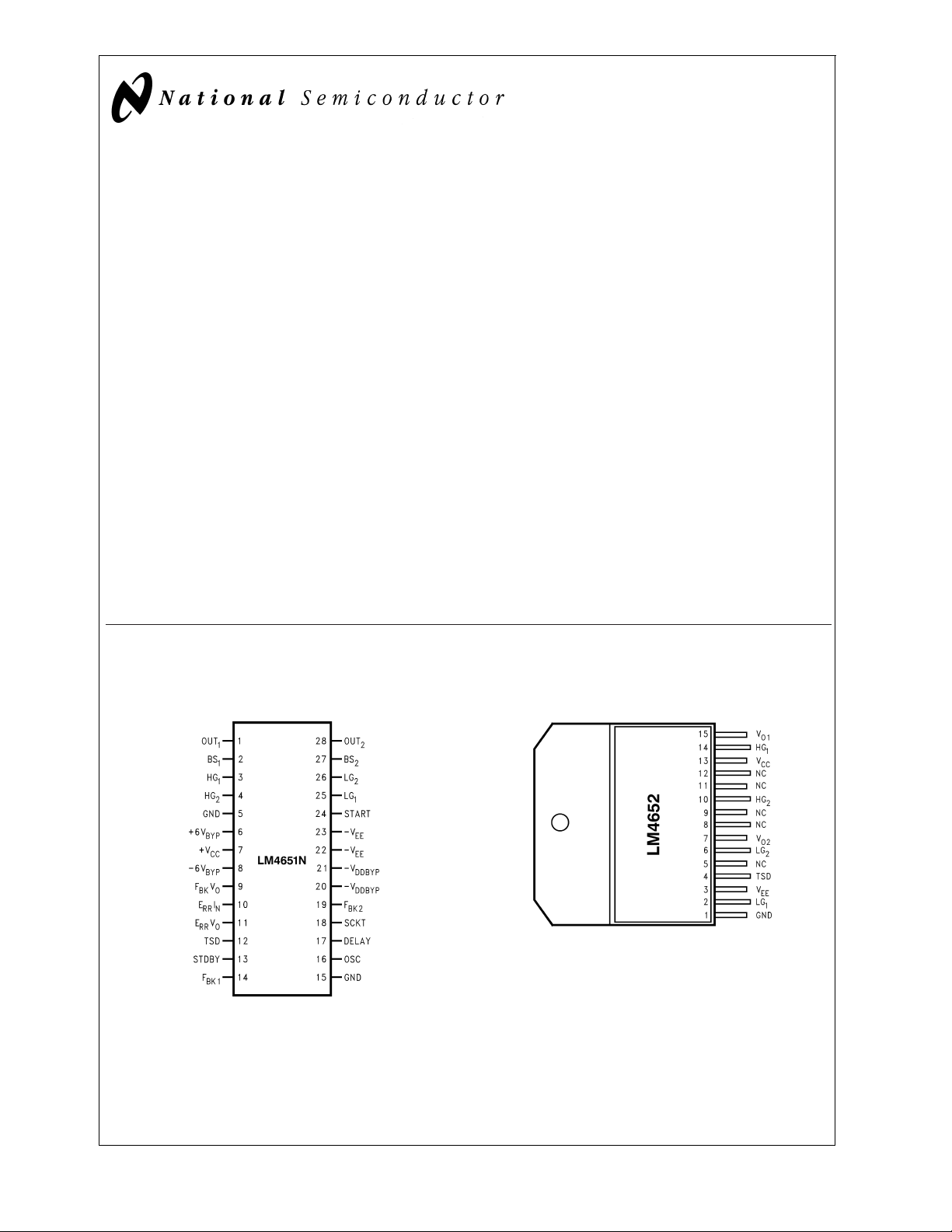
Connection Diagrams
LM4651 Plastic Package
Top View
Order Number LM4651N
See NS Package Number N28B
DS101277-72
LM4652 Plastic Package (Note 8)
DS101277-73
Isolated TO-220 Package
Order Number LM4652TF
See NS Package Number TF15B
or
Non-Isolated TO-220 Package
Order Number LM4652TA
See NS Package Number TA15A
Overture®is a registered trademark of National Semiconductor Corporation.
© 2001 National Semiconductor Corporation DS101277 www.national.com
Absolute Maximum Ratings (Notes 1, 2)
If Military/Aerospace specified devices are required,
please contact the National Semiconductor Sales Office/
Distributors for availability and specifications.
Supply Voltage
Output Current (LM4652) 10A
LM4651 & LM4652
Power Dissipation (LM4651) (Note 3) 1.5W
Power Dissipation (LM4652) (Note 3) 32W
±
22V
Operating Ratings (Notes 1, 2)
Temperature Range −40˚C ≤ T
Supply Voltage |V
Thermal Resistance
LM4651 N Package
θJA 52˚C/W
θJC 22˚C/W
+
|+|V−| 22V to 44V
ESD Susceptibility (LM4651) (Note 4) 2000V
LM4652 (pins 2,6,10,11) 500V
ESD Susceptibility (LM4651) (Note 5) 200V
LM4652 (pins 2,6,10,11) 100V
LM4652 TF, TO−220 Package
θJA 43˚C/W
θJC 2.0˚C/W
Junction Temperature (Note 6) 150˚C
Soldering Information
N, TA and TF Package (10 seconds) 260˚C
Storage Temperature −40˚C to + 150˚C
LM4652 T, TO−220 Package
θJA 37˚C/W
θJC 1.0˚C/W
System Electrical Characteristics for LM4651 and LM4652 (Notes 1, 2)
The following specifications apply for +VCC= +20V, −VEE= −20V, fSW= 125kHz, fIN= 100Hz, RL=4Ω, unless otherwise
specified. Typicals apply for T
Symbol Parameter Conditions
I
CQ
I
STBY
A
P
M
O
Total Quiescent Power Supply
Current
Standby Current V
Standby Attenuation V
Output Power (Continuous Average)
η Efficiency at P
η
Pd
Efficiency
(LM4651 & LM4652)
Power Dissipation
(LM4651 + LM4652)
THD+N Total Harmonic Distortion Plus Noise
e
OUT
Output Noise A Weighted, no signal, RL=4Ω 550 µV
SNR Signal-to-Noise Ratio
V
OS
Output Offset Voltage VIN= 0V, IO= 0mA, R
PSRR Power Supply Rejection Ratio
= 25˚C. For specific circuit values, refer to Figure 1 (Typical Audio Application Circuit).
A
Typical Units
= 0V, LO= 0mA, |I
V
CIN
R
DLY
R
DLY
13 = 5V, Stby: On 17 mA
PIN
13 = 5V, Stby: On
PIN
R
=4Ω, 1% THD 125 W
L
R
=4Ω, 10% THD 155 W
L
R
=8Ω, 1% THD 75 W
L
R
=8Ω, 10% THD 90 W
L
f
= 75kHz, RL=4Ω, 1% THD 135 W
SW
f
= 75kHz, RL=4Ω, 10% THD 170 W
SW
=5W PO= 5W, R
O
= 125W, THD = 1% 85 %
P
O
= 125W, THD = 1% (max) 22 W
P
O
f
= 75kHz, PO= 135W,
SW
=0Ω
= 10kΩ
=5kΩ 55 %
DLY
VCC+
|+|I
VEE−
|
THD = 1% (max)
10W, 10Hz ≤ f
≤ 500Hz, AV=18dB
IN
10Hz ≤ BW ≤ 80kHz
A-Wtg, P
22kHz BW, P
=4Ω, 10Hz ≤ BW ≤ 30kHz
R
L
+V
CC
= 125W, RL4Ω 92 dB
out
= 125W, RL4Ω 89 dB
out
=0Ω 0.7 V
OFFSET
AC
=−V
=1V
EE
RMS,fAC
AC
= 120Hz
LM4651 & LM4652
237
124
>
115 dB
22 W
0.3 %
37 dB
≤ +85˚C
A
mA
mA
www.national.com 2
Electrical Characteristics for LM4651 (Notes 1, 2, 7)
The following specifications apply for +VCC= +20V, −VEE= −20V, fSW= 125kHz, unless otherwise specified. Limits apply for
T
= 25˚C. For specific circuit values, refer to Figure 1 (Typical Audio Application Circuit).
A
Symbol Parameter Conditions
I
CQ
Standby
V
IL
V
IH
f
SW
f
SWerror
T
dead
T
OverMod
Total Quiescent Current
Standby Low Input Voltage Not in Standby Mode 0.8 V
Standby High Input Voltage In Standby Mode 2.5 2.0 V
Switching Frequency Range
50% Duty Cycle Error R
Dead Time R
Over Modulation Protection Time Pulse Width Measured at 50% 310 ns
LM4652 not connected, I
|+|I
|I
VCC+
R
= 15kΩ 65 kHz
OSC
R
=0Ω 200 kHz
OSC
=4kΩ,fSW= 125kHz 1 3 %
OSC
=0Ω 27 ns
DLY
VEE−
|, R
DLY
O
=0Ω
= 0mA,
Min Typical Max Units
15 36 45 mA
LM4651
Electrical Characteristics for LM4652 (Notes 1, 2, 7)
The following specifications apply for +VCC= +20V, −VEE= −20V, unless otherwise specified. Limits apply for TA= 25˚C. For
specific circuit values, refer to Figure 1 (Typical Audio Application Circuit).
Symbol Parameter Conditions
DSS
V
(BR)
I
DSS
VGS
th
R
DS(ON)
t
r
t
f
I
D
Note 1: Absolute Maximum Ratings indicate limits beyond which damage to the device may occur. Operating Ratings indicate conditions for which the device is
functional, but do not guarantee specific performance limits. Electrical Characteristics state DC and AC electrical specifications under particular test conditions which
guarantee specific performance limits. This assumes that the device is within the Operating Ratings. Specifications are not guaranteed for parameters where no limit
is given, however, the typical value is a good indication of device performance.
Note 2: All voltages are measured with respect to the GND pin unless otherwise specified.
Note 3: For operating at case temperatures above 25˚C, the LM4651 must be de−rated based on a 150˚C maximum junction temperature and a thermal resistance
of θ
2.0 ˚C/W (junction to case) for the isolated package (TF) or a thermal resistance of θ
Note 4: Human body model, 100 pF discharged through a 1.5 kΩ resistor.
Note 5: Machine Model, 220pF-240pF discharge through all pins.
Note 6: The operating junction temperature maximum, T
Note 7: Limits are guaranteed to National’s AOQL (Average Outgoing Quality Level).
Note 8: The LM4652TA package TA15A is a non-isolated package, setting the tab of the device and the heat sink at −V potential when the LM4652 is directly
mounted to the heat sink using only thermal compound. If a mica washer is used in addition to thermal compound, θ
will be isolated from −V.
Drain−to−Source Breakdown
Voltage
VGS = 0 55 V
Drain−to−Source Leakage Current VDS = 44VDC, VGS = 0V 1.0 mA
Gate Threshold Voltage VDS = VGS, ID = 1mA
Static Drain−to−Source On
Resistance
Rise Time
Fall Time
Maximum Saturation Drain
Current
= 62 ˚C/W (junction to ambient), while the LM4652 must be de−rated based on a 150˚C maximum junction temperature and a thermal resistance of θJC=
JA
VGS=6V
VGD=6V
=0Ω
VGD=6V
=0Ω
VGS=6V
is 150˚C.
jmax
,ID=6A
DC
, VDS = 40VDC,R
DC
, VDS = 40VDC,R
DC
, VDS = 10V
DC
DC
DC
GATE
GATE
DC
= 1.0˚C/W (junction to case) for the non-isolated package (T).
JC
Min Typical Max Units
810 A
(case to sink) is increased, but the heat sink
CS
LM4652
0.85 V
200 300 mΩ
25 ns
26 ns
LM4651 & LM4652
DC
www.national.com3
Electrical Characteristics for LM4652 (Notes 1, 2, 7) (Continued)
LM4651 & LM4652
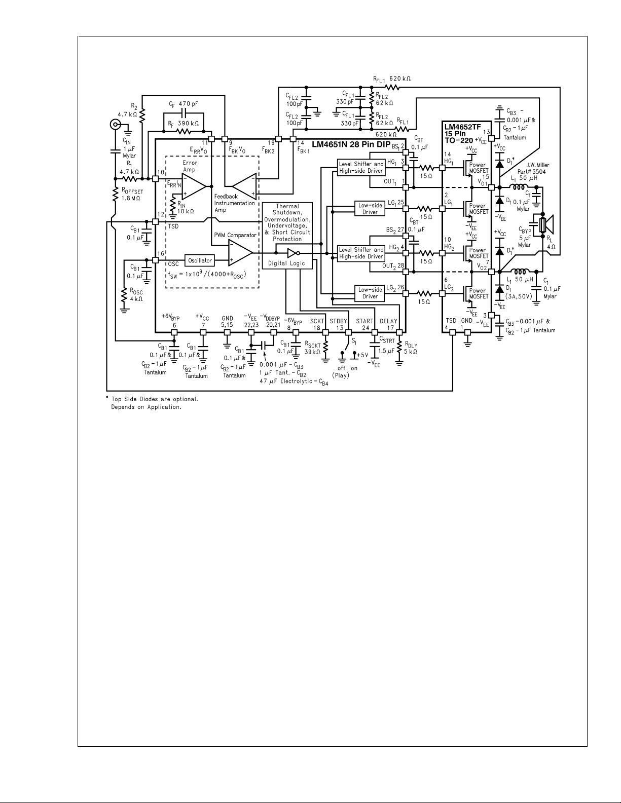
FIGURE 1. Typical Application Circuit and Test Circuit
DS101277-68
www.national.com 4
LM4651 Pin Descriptions
Pin No. Symbol Description
1 OUT
2,27 BS
3HG
4HG
1
,BS
1
2
1
2
5,15 GND The ground pin for all analog circuitry.
6 +6V
7+V
8 −6V
9F
10 E
11 E
BYP
CC
BYP
BKVO
RRIN
RRVO
12 TSD The thermal shut down input pin for the thermal shut down output of the LM4652.
13 STBY Standby function input pin. This pin is CMOS compatible.
14 FBK
1
16 OSC
17 Delay The dead time setting pin.
18 SCKT Short circuit setting pin. Minimum setting is 10A.
19 FBK
20,21 −V
22,23 −V
2
DDBYP
EE
24 START
25 LG
26 LG
28 OUT
1
2
2
The reference pin of the power MOSFET output to the gate drive circuitry.
The bootstrap pin provides extra bias to drive the upper gates, HG1,HG2.
High−Gate#1 is the gate drive to a top side MOSFET in the H-Bridge.
High−Gate#2 is the gate drive to a top side MOSFET in the H-Bridge.
The internally regulated positive voltage output for analog circuitry. This pin is available
for internal regulator bypassing only.
The positive supply input for the IC.
The internally regulated negative voltage output for analog circuitry. This pin is available
for internal regulator bypassing only.
The feedback instrumentation amplifier output pin.
The error amplifier inverting input pin. The input audio signal and the feedback signal are
summed at this input pin.
The error amplifier output pin.
The feedback instrumentation amplifier pin. This must be connected to the feedback filter
from V
(pin 15 on the LM4652 ).
O1
The switching frequency oscillation pin. Adjusting the resistor from 15.5kΩ to 0Ω
changes the switching frequency from 75kHz to 225kHz.
The feedback instrumentation amplifier pin. This must be connected to the feedback filter
from V
(pin 7 on the LM4652 ).
O2
The regulator output for digital blocks. This pin is for bypassing only.
The negative voltage supply pin for the IC.
The start up capacitor input pin. This capacitor adjusts the start up time of the diagnostic
sequence for the modulator. Refer to Start up Sequence and Timing in the
Application Information section.
Low−Gate#1 is the gate drive to a bottom side MOSFET in the H-Bridge.
Low−Gate#2 is the gate drive to a bottom side MOSFET in the H-Bridge.
The reference pin of the power MOSFET output to the gate drive circuitry.
LM4651 & LM4652
www.national.com5
LM4652 Pin Descriptions
Pin No. Symbol Description
1 GND A ground reference for the thermal shut down circuitry.
LM4651 & LM4652
2LG
3−V
1
EE
4 TSD
Low−Gate#1 is the gate input to a bottom side MOSFET in the H-Bridge.
The negative voltage supply input for the power MOSFET H-Bridge.
The thermal shut down flag pin. This pin transitions to 6V when the die temperature
exceeds 150˚C.
5 NC No connection
6LG
7VO
2
2
Low−Gate#2 is the gate input to a bottom side MOSFET in the H-Bridge.
The switching output pin for one side of the H-Bridge.
8 NC No connection.
9 NC No connection.
10 HG
2
High−Gate#2 is the gate input to a top side MOSFET in the H-Bridge.
11 NC No connection.
12 NC No connection.
13 +V
14 HG
15 VO
CC
1
2
The positive voltage supply input for the power MOSFET H-Bridge.
High−Gate#1 is the gate input to a top side MOSFET in the H-Bridge.
The switching output pin for one side of the H-Bridge.
Note: NC, no connect pins are floating pins. It is best to connect the pins to GND to minimize any noise from being coupled into
the pins.
External Components Description (Refer to Figure 1)
Components Functional Description
1. R
2. R
3. R
4. C
1
2
f
f
Works with R2,R
)/ R
R
)−(R2/R1) + .5].
fl2
fl2
See description above for R1.
Sets the gain and bandwidth of the system by creating a low pass filter for the Error
Amplifier’s feedback with C
See description above for Rf.
fl1
and R
to set the gain of the system. Gain = [(R2/R1) x ((R
fl2
. 3dB pole is at fC= 1/(2πRfCf) (Hz).
f
Provides a reduction in the feedback with R
5. R
fI1
reduce effects on the pole created by R
fI2
System Gain.
6. R
7. C
8. R
9. C
10. L
11. C
12. C
byp
and C
fI2
fI1
fI3
fI2
1
1
fI2
note for R
See description above for R
Establish the second pole for the low pass filter in the feedback path at fC=
1/(2πR
See description above for R
Combined with C
= 1/[2π(L12C
Filters high frequency noise from the amplifier’s output to ground. Recommended value
is 0.1µF to 1µF.
See description for L1.
creates a low pass filter with a pole at fC= 1/(2πR
fI1
for effect on System Gain.
1,R2
.
fI2
) (Hz).
fI3CfI2
.
fI3
creates a 2−pole, low pass output filter that has a −3dB pole at f
BYP
1
)
⁄
2
] (Hz).
BYP
R
Bypass capacitors for VCC,VEE, analog and digital voltages (VDD, +6V, −6V). See
13. C
B1−CB4
Supply Bypassing and High Frequency PCB Design in the Application Information
section for more information.
14. B
15. R
16. C
START
17. R
18. R
19. D
BT
DLY
SCKT
OSC
1
Provides the bootstrap capacitance for the boot strap pin.
Sets the dead time or break before make to T
Controls the startup time with T
Sets the output short circuit current with I
START
= (8.5x10⁴)C
SCKT
Controls the switching frequency with fSW=1X10⁹/ (4000 + R
Schottky diode to protect the output MOSFETs from fly back voltages.
should be 10 X R
fI2.RfI1
and C
. See also note for R1,R2for effect on
fI1
= (1.7x10
DLY
START
= (1x10⁵)/ (10kΩ\ R
fI2CfI1
−12
)(500+R
(seconds).
OSC
minimum to
fI2
) (Hz). See also
) (seconds).
DLY
) (A).
SCKT
) (Hz).
+
fl1
C
www.national.com 6
 Loading...