May 2007
LM4562
Dual High Performance, High Fidelity Audio Operational
Amplifier
General Description
The LM4562 is part of the ultra-low distortion, low noise, high
slew rate operational amplifier series optimized and fully
specified for high performance, high fidelity applications.
Combining advanced leading-edge process technology with
state-of-the-art circuit design, the LM4562 audio operational
amplifiers deliver superior audio signal amplification for outstanding audio performance. The LM4562 combines extremely low voltage noise density (2.7nV/√Hz
) with vanishingly low THD+N (0.00003%) to easily satisfy the most
demanding audio applications. To ensure that the most challenging loads are driven without compromise, the LM4562
has a high slew rate of ±20V/μs and an output current capability of ±26mA. Further, dynamic range is maximized by an
output stage that drives 2kΩ loads to within 1V of either power
supply voltage and to within 1.4V when driving 600Ω loads.
The LM4562's outstanding CMRR (120dB), PSRR (120dB),
and VOS (0.1mV) give the amplifier excellent operational amplifier DC performance.
The LM4562 has a wide supply range of ±2.5V to ±17V. Over
this supply range the LM4562’s input circuitry maintains excellent common-mode and power supply rejection, as well as
maintaining its low input bias current. The LM4562 is unity
gain stable. This Audio Operational Amplifier achieves outstanding AC performance while driving complex loads with
values as high as 100pF.
The LM4562 is available in 8–lead narrow body SOIC, 8–lead
Plastic DIP, and 8–lead Metal Can TO-99. Demonstration
boards are available for each package.
Key Specifications
■ Power Supply Voltage Range ±2.5V to ±17V
■
THD+N (AV = 1, V
OUT
= 3V
RMS
, fIN = 1kHz)
RL = 2kΩ
0.00003% (typ)
RL = 600Ω
0.00003% (typ)
■ Input Noise Density 2.7nV/√Hz (typ)
■ Slew Rate
±20V/μs (typ)
■ Gain Bandwidth Product
55MHz (typ)
■ Open Loop Gain (R
L
= 600Ω)
140dB (typ)
■ Input Bias Current
10nA (typ)
■ Input Offset Voltage
0.1mV (typ)
■ DC Gain Linearity Error
0.000009%
Features
■
Easily drives 600Ω loads
■
Optimized for superior audio signal fidelity
■
Output short circuit protection
■
PSRR and CMRR exceed 120dB (typ)
■
SOIC, DIP, TO-99 metal can packages
Applications
■
Ultra high quality audio amplification
■
High fidelity preamplifiers
■
High fidelity multimedia
■
State of the art phono pre amps
■
High performance professional audio
■
High fidelity equalization and crossover networks
■
High performance line drivers
■
High performance line receivers
■
High fidelity active filters
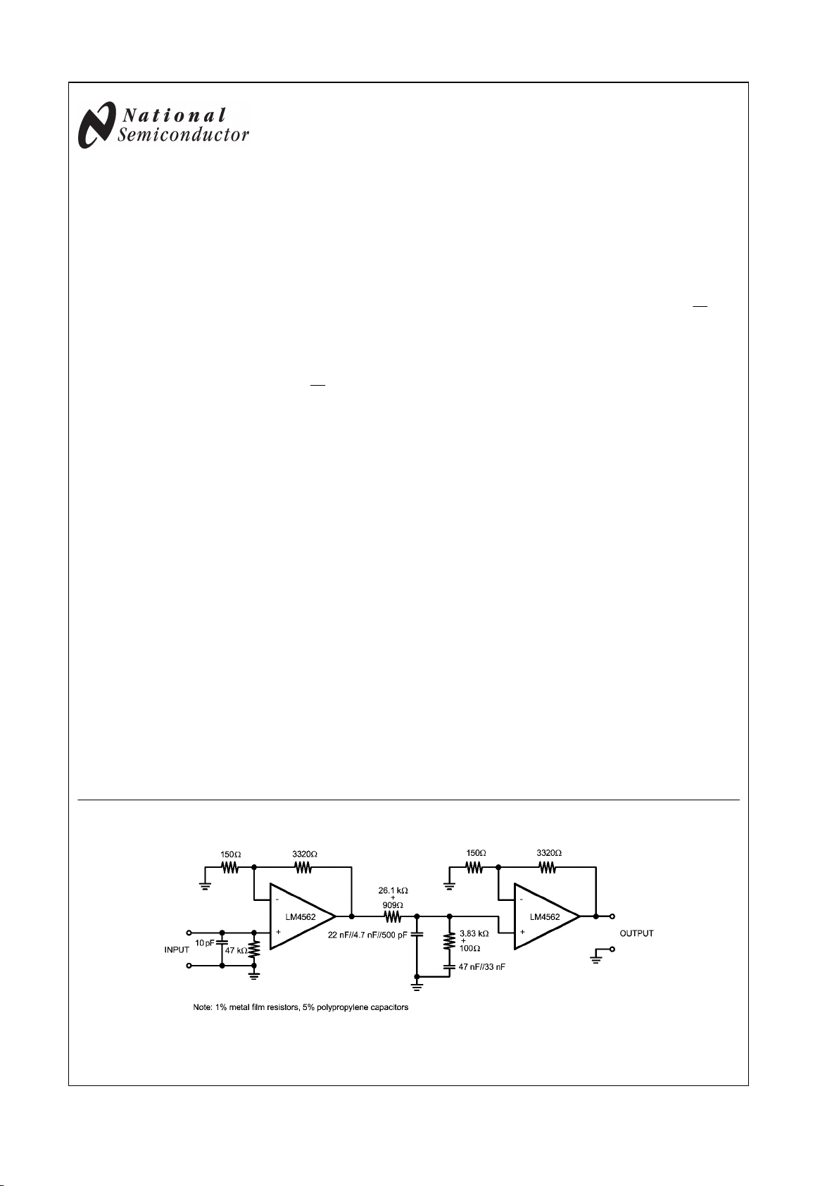
Typical Application
201572k5
Passively Equalized RIAA Phono Preamplifier
© 2007 National Semiconductor Corporation 201572 www.national.com
LM4562 Dual High Performance, High Fidelity Audio Operational Amplifier
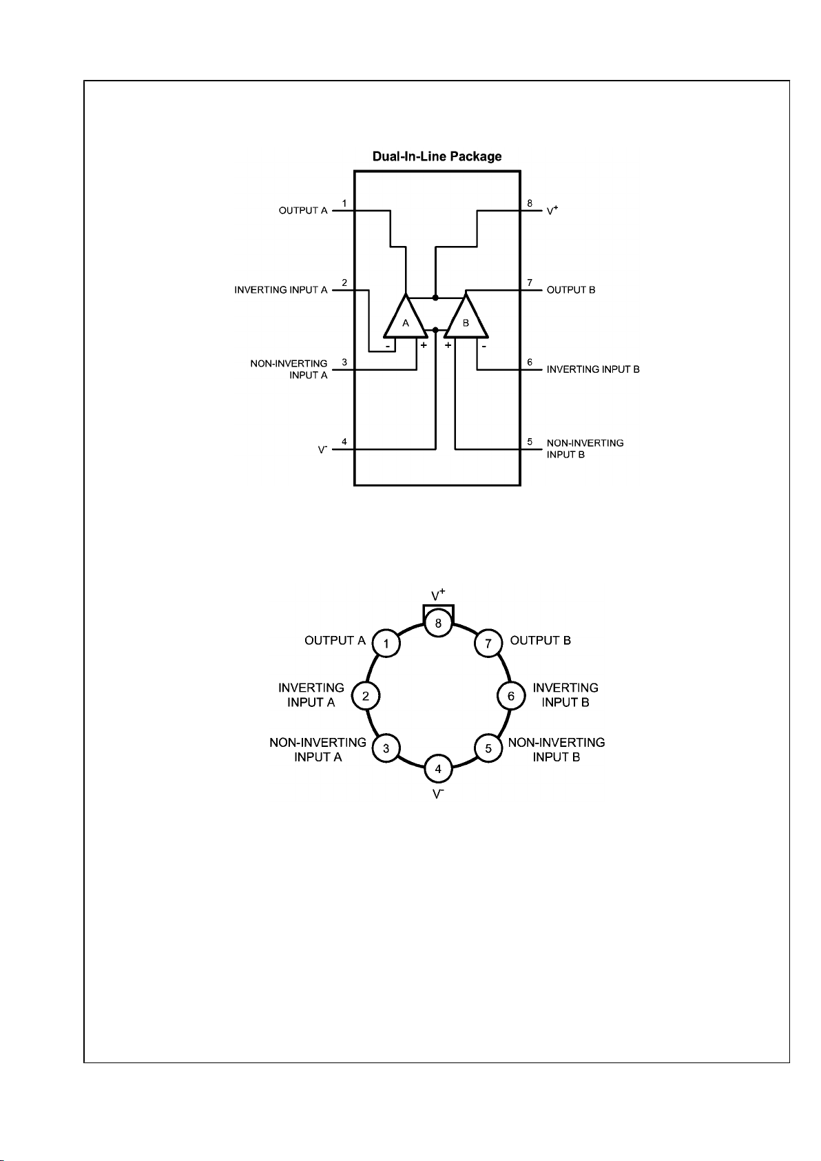
Connection Diagrams
20157255
Order Number LM4562MA
See NS Package Number — M08A
Order Number LM4562NA
See NS Package Number — N08E
Metal Can
201572f3
Order Number LM4562HA
See NS Package Number — H08C
www.national.com 2
LM4562
Absolute Maximum Ratings (Notes 1, 2)
If Military/Aerospace specified devices are required,
please contact the National Semiconductor Sales Office/
Distributors for availability and specifications.
Power Supply Voltage
(VS = V+ - V-)
36V
Storage Temperature −65°C to 150°C
Input Voltage
(V-) - 0.7V to (V+) + 0.7V
Output Short Circuit (Note 3) Continuous
Power Dissipation Internally Limited
ESD Susceptibility (Note 4) 2000V
ESD Susceptibility (Note 5)
Pins 1, 4, 7 and 8 200V
Pins 2, 3, 5 and 6 100V
Junction Temperature 150°C
Thermal Resistance
θJA (SO)
145°C/W
θJA (NA)
102°C/W
θJA (HA)
150°C/W
θJC (HA)
35°C/W
Temperature Range
T
MIN
≤ TA ≤ T
MAX
–40°C ≤ TA ≤ 85°C
Supply Voltage Range
±2.5V ≤ VS ≤ ± 17V
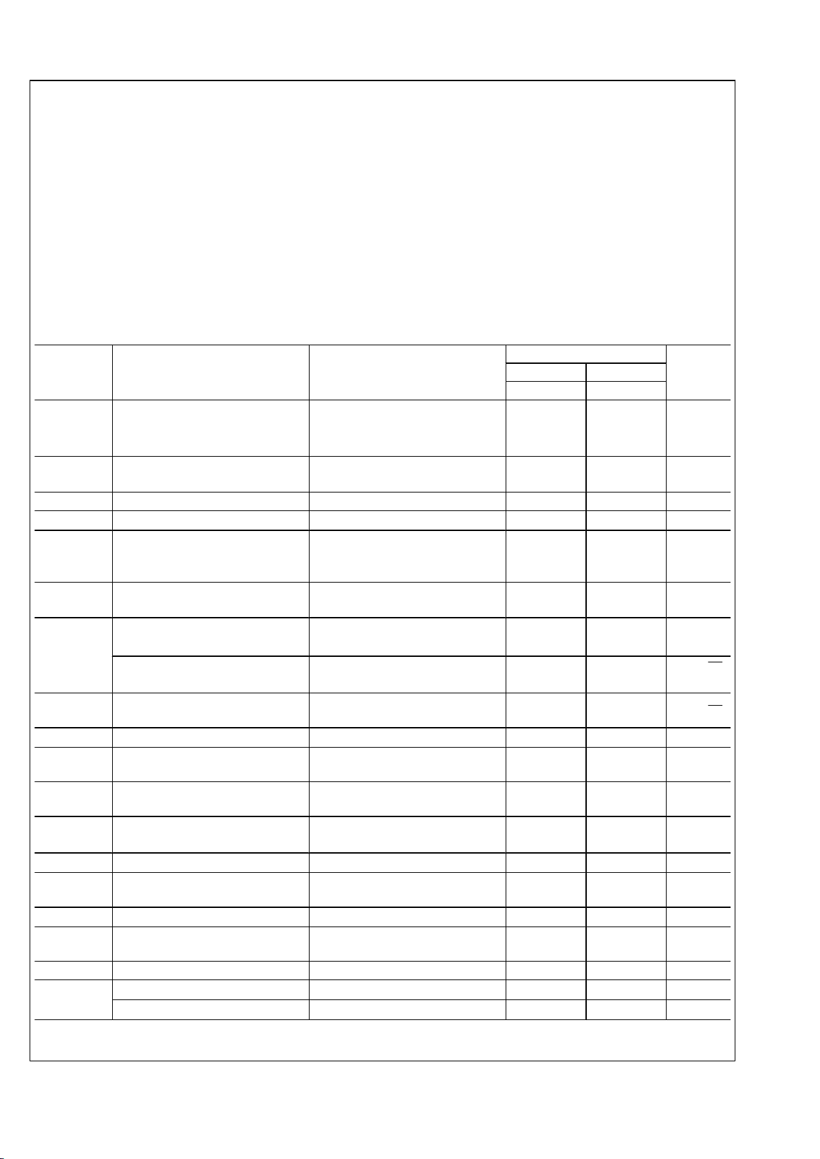
Electrical Characteristics for the LM4562 (Notes 1, 2) The specifications apply for V
S
= ±15V, RL =
2kΩ, fIN = 1kHz, TA = 25°C, unless otherwise specified.
Symbol Parameter Conditions
LM4562
Units
(Limits)
Typical Limit
(Note 6) (Note 7)
THD+N Total Harmonic Distortion + Noise
AV = 1, V
OUT
= 3V
rms
RL = 2kΩ
RL = 600Ω
0.00003
0.00003 0.00009
% (max)
IMD Intermodulation Distortion
AV = 1, V
OUT
= 3V
RMS
Two-tone, 60Hz & 7kHz 4:1
0.00005 %
GBWP Gain Bandwidth Product 55 45 MHz (min)
SR Slew Rate ±20 ±15
V/μs (min)
FPBW Full Power Bandwidth
V
OUT
= 1V
P-P
, –3dB
referenced to output magnitude
at f = 1kHz
10
MHz
t
s
Settling time
AV = –1, 10V step, CL = 100pF
0.1% error range
1.2
μs
e
n
Equivalent Input Noise Voltage fBW = 20Hz to 20kHz 0.34 0.65
μV
RMS
(max)
Equivalent Input Noise Density
f = 1kHz
f = 10Hz
2.7
6.4
4.7
nV/√Hz
(max)
i
n
Current Noise Density
f = 1kHz
f = 10Hz
1.6
3.1
pA/√Hz
V
OS
Offset Voltage ±0.1 ±0.7 mV (max)
ΔVOS/ΔTemp
Average Input Offset Voltage Drift vs
Temperature
–40°C ≤ TA ≤ 85°C
0.2
μV/°C
PSRR
Average Input Offset Voltage Shift vs
Power Supply Voltage
ΔVS = 20V (Note 8)
120 110 dB (min)
ISO
CH-CH
Channel-to-Channel Isolation
fIN = 1kHz
fIN = 20kHz
118
112
dB
I
B
Input Bias Current VCM = 0V 10 72 nA (max)
ΔIOS/ΔTemp
Input Bias Current Drift vs
Temperature
–40°C ≤ TA ≤ 85°C
0.1
nA/°C
I
OS
Input Offset Current VCM = 0V 11 65 nA (max)
V
IN-CM
Common-Mode Input Voltage Range
+14.1
–13.9
(V+) – 2.0
(V-) + 2.0
V (min)
CMRR Common-Mode Rejection –10V<Vcm<10V 120 110 dB (min)
Z
IN
Differential Input Impedance
30
kΩ
Common Mode Input Impedance –10V<Vcm<10V 1000
MΩ
3 www.national.com
LM4562
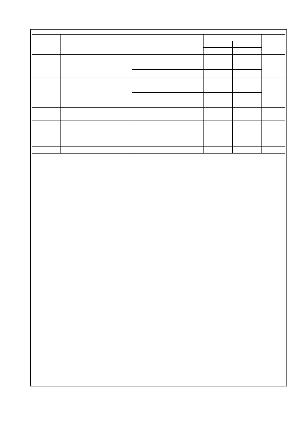
Symbol Parameter Conditions
LM4562
Units
(Limits)
Typical Limit
(Note 6) (Note 7)
A
VOL
Open Loop Voltage Gain
–10V<Vout<10V, RL = 600Ω
140 125
dB (min)
–10V<Vout<10V, RL = 2kΩ
140
–10V<Vout<10V, RL = 10kΩ
140
V
OUTMAX
Maximum Output Voltage Swing
RL = 600Ω
±13.6 ±12.5
V (min)
RL = 2kΩ
±14.0
RL = 10kΩ
±14.1
I
OUT
Output Current
RL = 600Ω, VS = ±17V
±26 ±23 mA (min)
I
OUT-CC
Instantaneous Short Circuit Current
+53
–42
mA
R
OUT
Output Impedance
fIN = 10kHz
Closed-Loop
Open-Loop
0.01
13
Ω
C
LOAD
Capacitive Load Drive Overshoot 100pF 16
%
I
S
Total Quiescent Current I
OUT
= 0mA 10 12 mA (max)
Note 1: Absolute Maximum Ratings indicate limits beyond which damage to the device may occur.
Note 2: Operating Ratings indicate conditions for which the device is functional, but do not guarantee specific performance limits. For guaranteed specifications
and test conditions, see the Electrical Characteristics. The guaranteed specifications apply only for the test conditions listed. Some performance characteristics
may degrade when the device is not operated under the listed test conditions.
Note 3: Amplifier output connected to GND, any number of amplifiers within a package.
Note 4: Human body model, 100pF discharged through a 1.5kΩ resistor.
Note 5: Machine Model ESD test is covered by specification EIAJ IC-121-1981. A 200pF cap is charged to the specified voltage and then discharged directly into
the IC with no external series resistor (resistance of discharge path must be under 50Ω).
Note 6: Typical specifications are specified at +25ºC and represent the most likely parametric norm.
Note 7: Tested limits are guaranteed to National's AOQL (Average Outgoing Quality Level).
Note 8: PSRR is measured as follows: VOS is measured at two supply voltages, ±5V and ±15V. PSRR = | 20log(ΔVOS/ΔVS) |.
www.national.com 4
LM4562
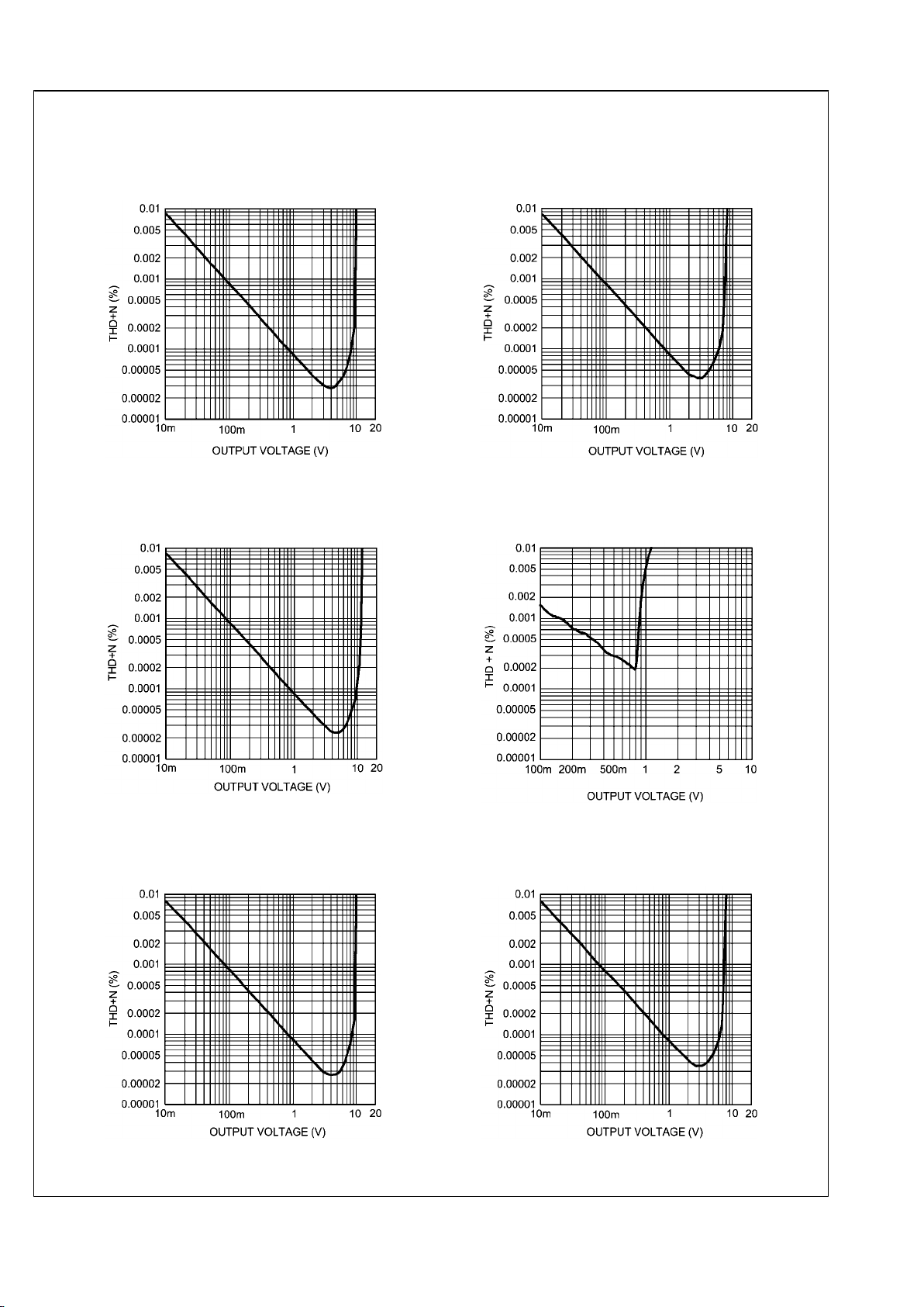
Typical Performance Characteristics
THD+N vs Output Voltage
VCC = 15V, VEE = –15V
RL = 2kΩ
201572k6
THD+N vs Output Voltage
VCC = 12V, VEE = –12V
RL = 2kΩ
201572k7
THD+N vs Output Voltage
VCC = 17V, VEE = –17V
RL = 2kΩ
201572k8
THD+N vs Output Voltage
VCC = 2.5V, VEE = –2.5V
RL = 2kΩ
201572i4
THD+N vs Output Voltage
VCC = 15V, VEE = –15V
RL = 600Ω
201572k9
THD+N vs Output Voltage
VCC = 12V, VEE = –12V
RL = 600Ω
201572l0
5 www.national.com
LM4562
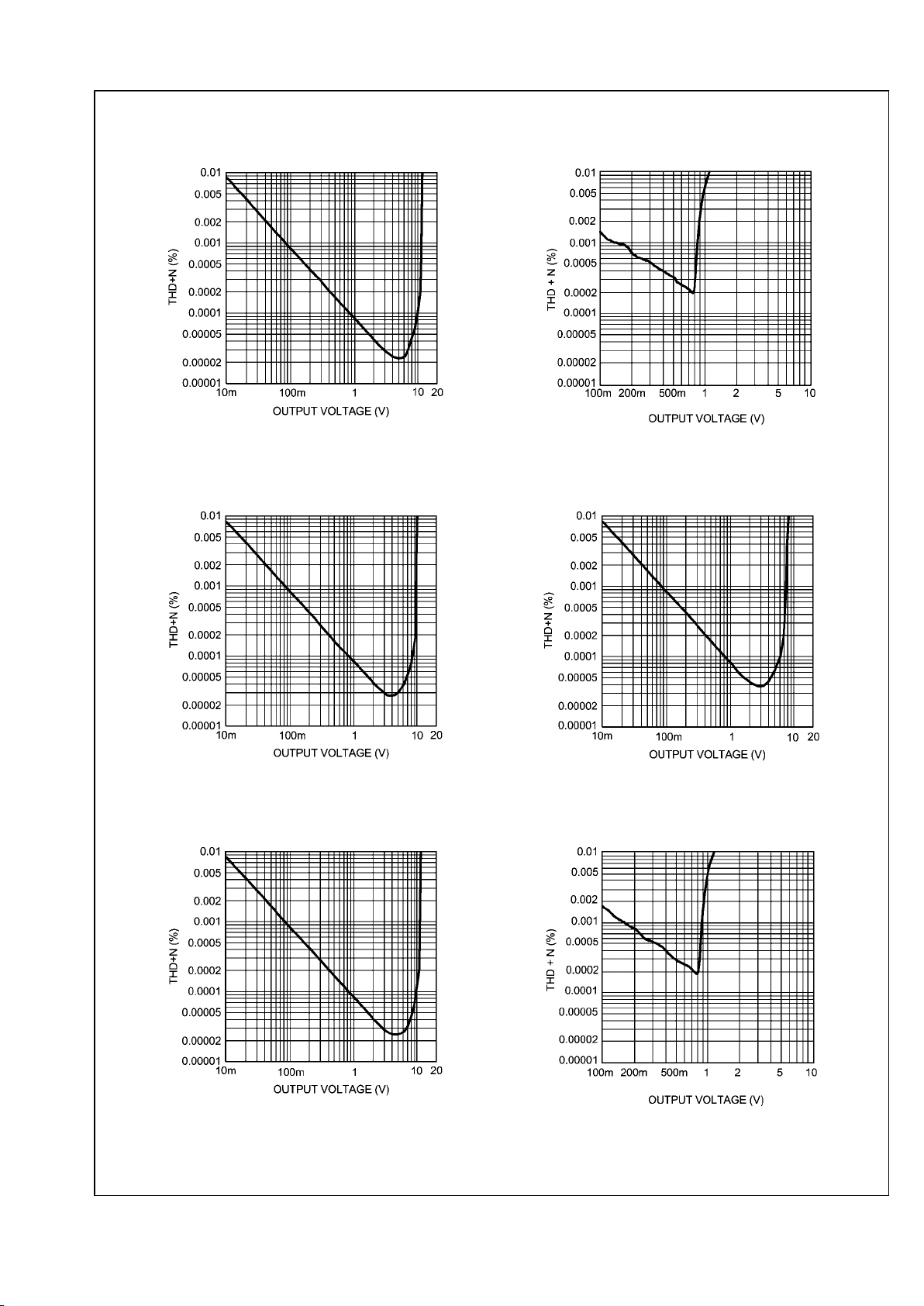
THD+N vs Output Voltage
VCC = 17V, VEE = –17V
RL = 600Ω
201572l1
THD+N vs Output Voltage
VCC = 2.5V, VEE = –2.5V
RL = 600Ω
201572i6
THD+N vs Output Voltage
VCC = 15V, VEE = –15V
RL = 10kΩ
201572l2
THD+N vs Output Voltage
VCC = 12V, VEE = –12V
RL = 10kΩ
201572l3
THD+N vs Output Voltage
VCC = 17V, VEE = –17V
RL = 10kΩ
201572l4
THD+N vs Output Voltage
VCC = 2.5V, VEE = –2.5V
RL = 10kΩ
201572i5
www.national.com 6
LM4562
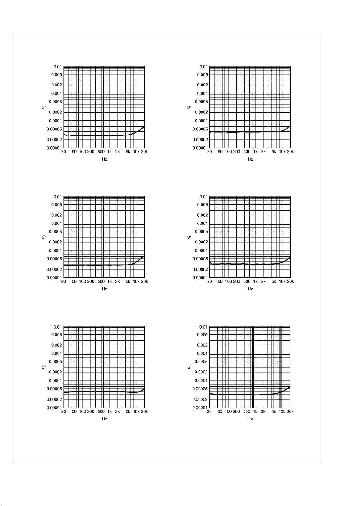
THD+N vs Frequency
VCC = 15V, VEE = –15V, V
OUT
= 3V
RMS
RL = 2kΩ
20157263
THD+N vs Frequency
VCC = 12V, VEE = –12V, V
OUT
= 3V
RMS
RL = 2kΩ
20157262
THD+N vs Frequency
VCC = 17V, VEE = –17V, V
OUT
= 3V
RMS
RL = 2kΩ
20157264
THD+N vs Frequency
VCC = 15V, VEE = –15V, V
OUT
= 3V
RMS
RL = 600Ω
20157259
THD+N vs Frequency
VCC = 12V, VEE = –12V, V
OUT
= 3V
RMS
RL = 600Ω
201572k3
THD+N vs Frequency
VCC = 17V, VEE = –17V, V
OUT
= 3V
RMS
RL = 600Ω
20157260
7 www.national.com
LM4562
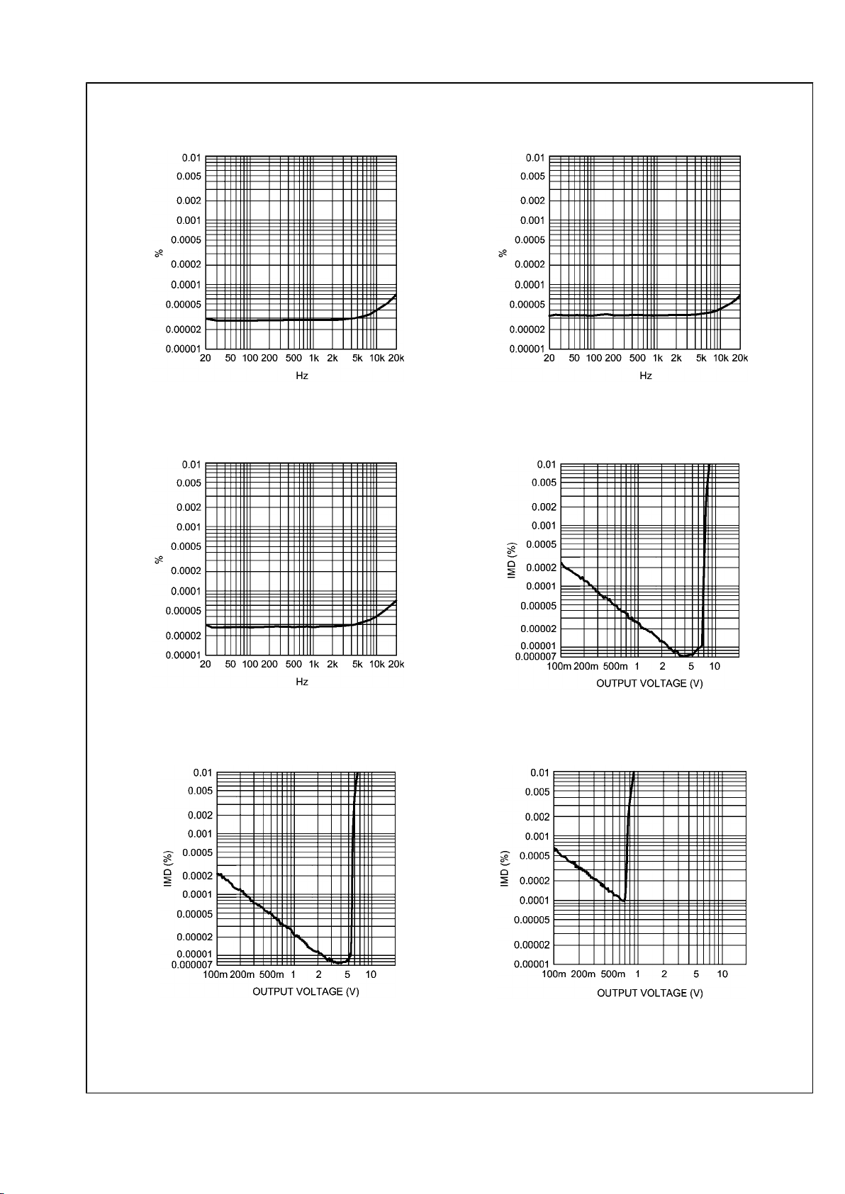
THD+N vs Frequency
VCC = 15V, VEE = –15V, V
OUT
= 3V
RMS
RL = 10kΩ
20157267
THD+N vs Frequency
VCC = 12V, VEE = –12V, V
OUT
= 3V
RMS
RL = 10kΩ
20157266
THD+N vs Frequency
VCC = 17V, VEE = –17V, V
OUT
= 3V
RMS
RL = 10kΩ
20157268
IMD vs Output Voltage
VCC = 15V, VEE = –15V
RL = 2kΩ
201572e6
IMD vs Output Voltage
VCC = 12V, VEE = –12V
RL = 2kΩ
201572e5
IMD vs Output Voltage
VCC = 2.5V, VEE = –2.5V
RL = 2kΩ
201572e4
www.national.com 8
LM4562
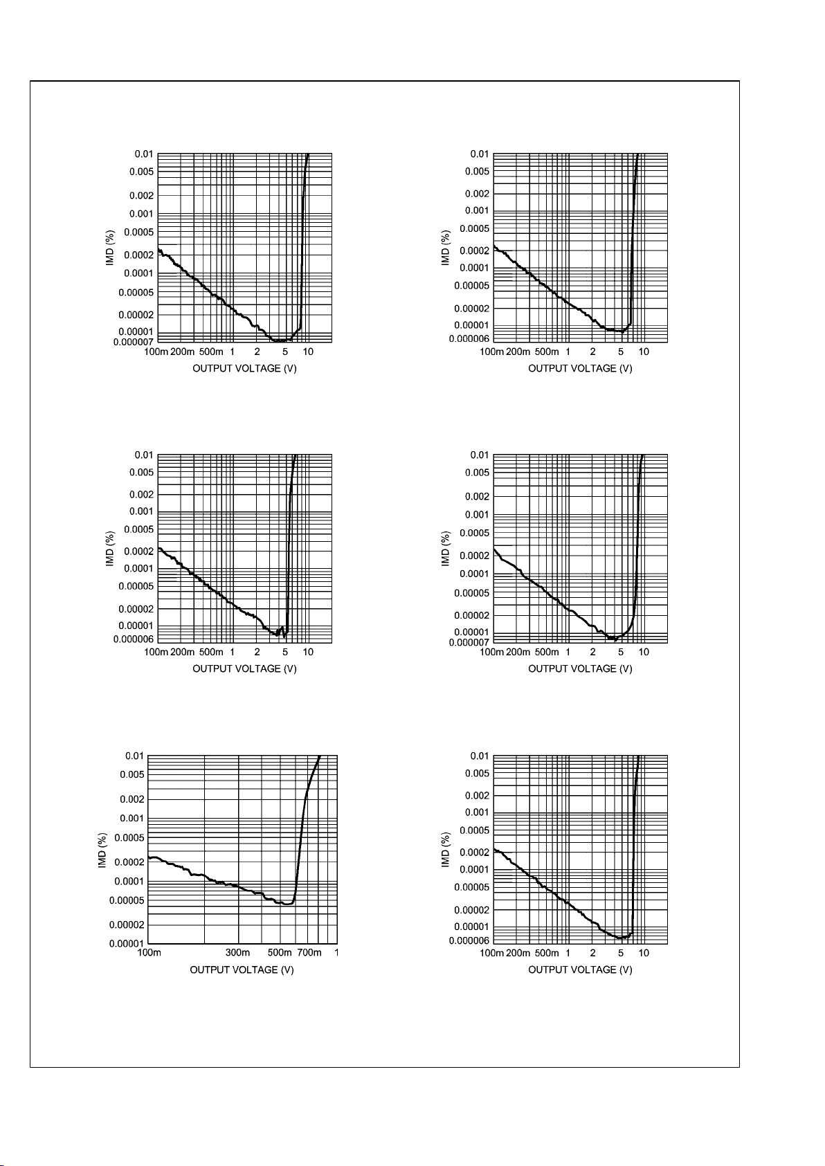
IMD vs Output Voltage
VCC = 17V, VEE = –17V
RL = 2kΩ
201572e7
IMD vs Output Voltage
VCC = 15V, VEE = –15V
RL = 600Ω
201572e2
IMD vs Output Voltage
VCC = 12V, VEE = –12V
RL = 600Ω
201572e0
IMD vs Output Voltage
VCC = 17V, VEE = –17V
RL = 600Ω
201572e3
IMD vs Output Voltage
VCC = 2.5V, VEE = –2.5V
RL = 600Ω
201572e1
IMD vs Output Voltage
VCC = 15V, VEE = –15V
RL = 10kΩ
201572f1
9 www.national.com
LM4562
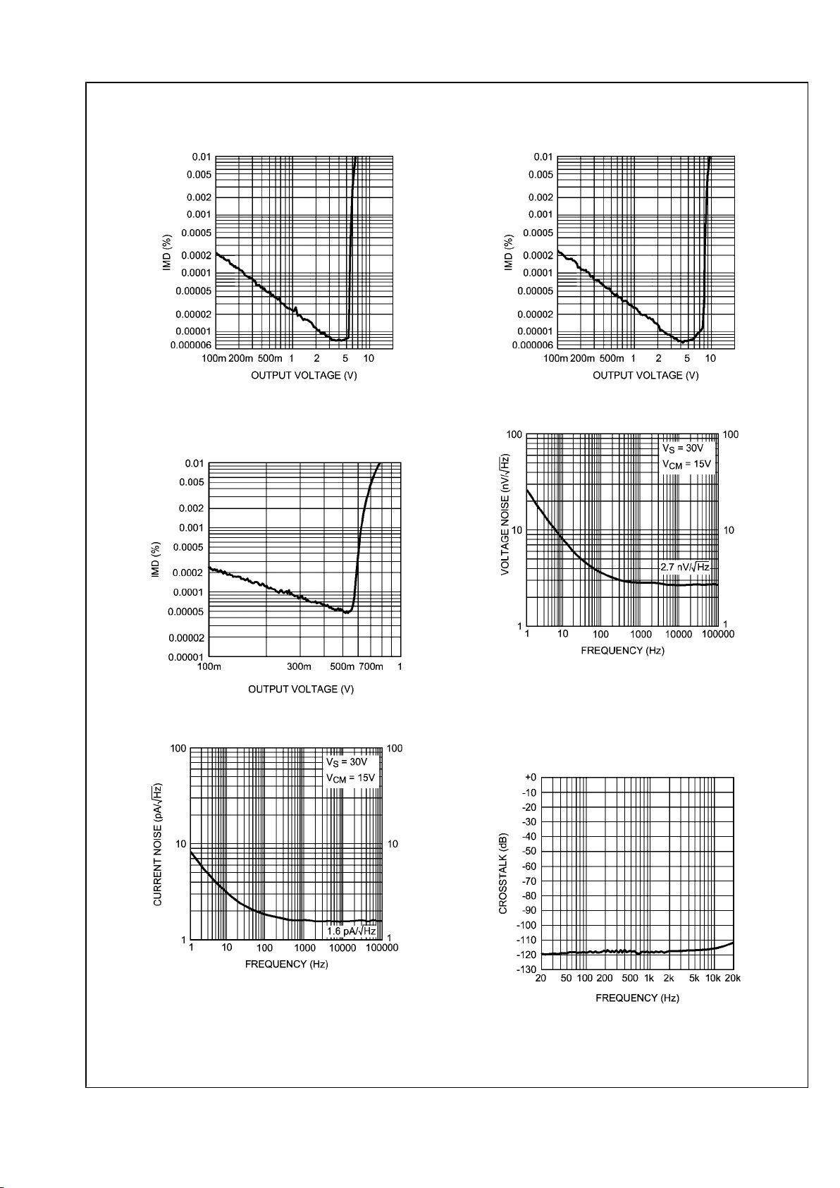
IMD vs Output Voltage
VCC = 12V, VEE = –12V
RL = 10kΩ
201572f0
IMD vs Output Voltage
VCC = 17V, VEE = –17V
RL = 10kΩ
201572f2
IMD vs Output Voltage
VCC = 2.5V, VEE = –2.5V
RL = 10kΩ
201572l6
Voltage Noise Density vs Frequency
201572h6
Current Noise Density vs Frequency
201572h7
Crosstalk vs Frequency
VCC = 15V, VEE = –15V, V
OUT
= 3V
RMS
AV = 0dB, RL = 2kΩ
201572c8
www.national.com 10
LM4562
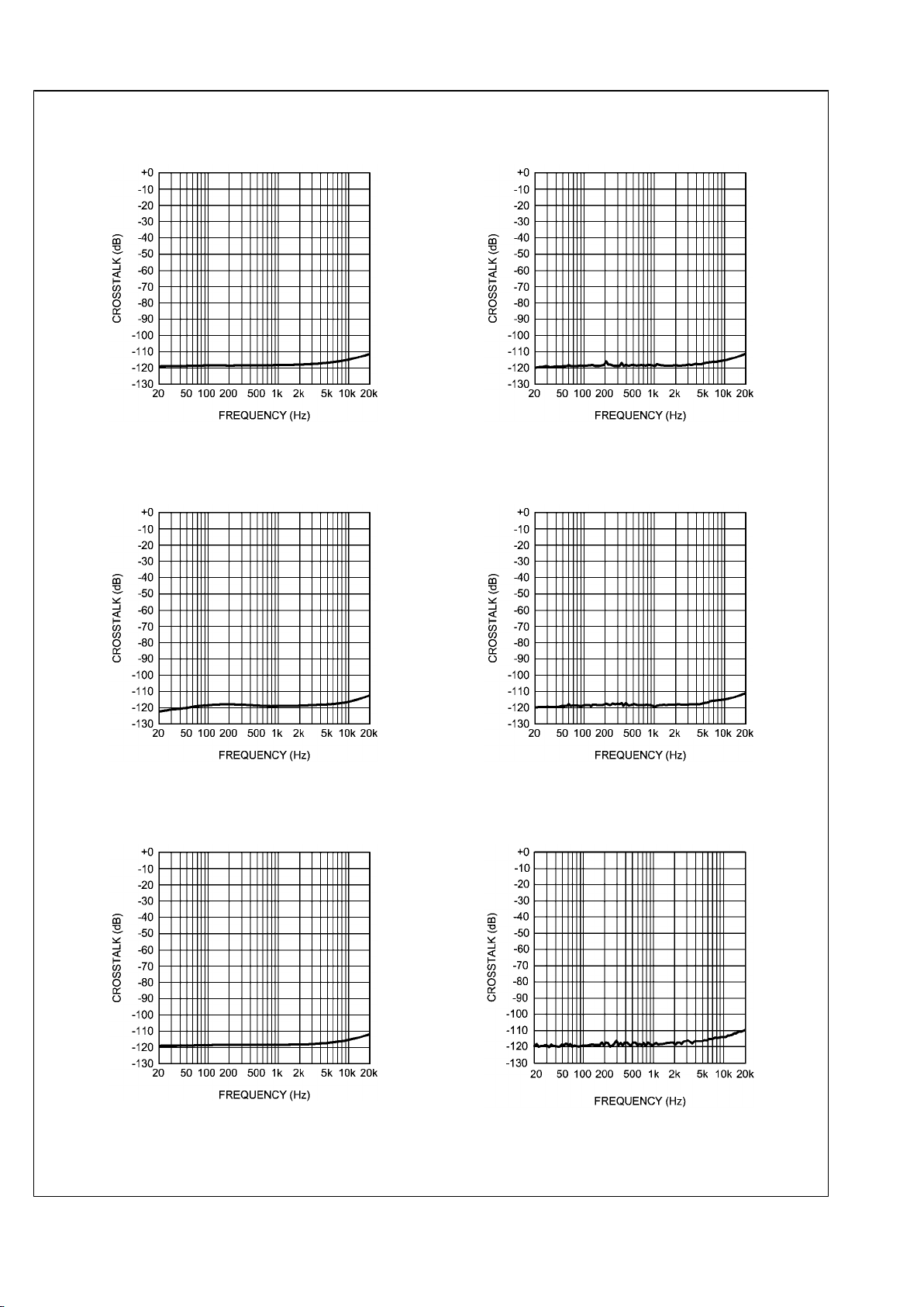
Crosstalk vs Frequency
VCC = 15V, VEE = –15V, V
OUT
= 10V
RMS
AV = 0dB, RL = 2kΩ
201572c9
Crosstalk vs Frequency
VCC = 12V, VEE = –12V, V
OUT
= 3V
RMS
AV = 0dB, RL = 2kΩ
201572c6
Crosstalk vs Frequency
VCC = 12V, VEE = –12V, V
OUT
= 10V
RMS
AV = 0dB, RL = 2kΩ
201572c7
Crosstalk vs Frequency
VCC = 17V, VEE = –17V, V
OUT
= 3V
RMS
AV = 0dB, RL = 2kΩ
201572d0
Crosstalk vs Frequency
VCC = 17V, VEE = –17V, V
OUT
= 10V
RMS
AV = 0dB, RL = 2kΩ
201572d1
Crosstalk vs Frequency
VCC = 2.5V, VEE = –2.5V, V
OUT
= 1V
RMS
AV = 0dB, RL = 2kΩ
201572n8
11 www.national.com
LM4562
 Loading...