

NSC LM4548VHX, LM4548VH Datasheet
LM4548
AC ’97 Rev 2 Codec with Sample Rate Conversion and
National 3D Sound
General Description
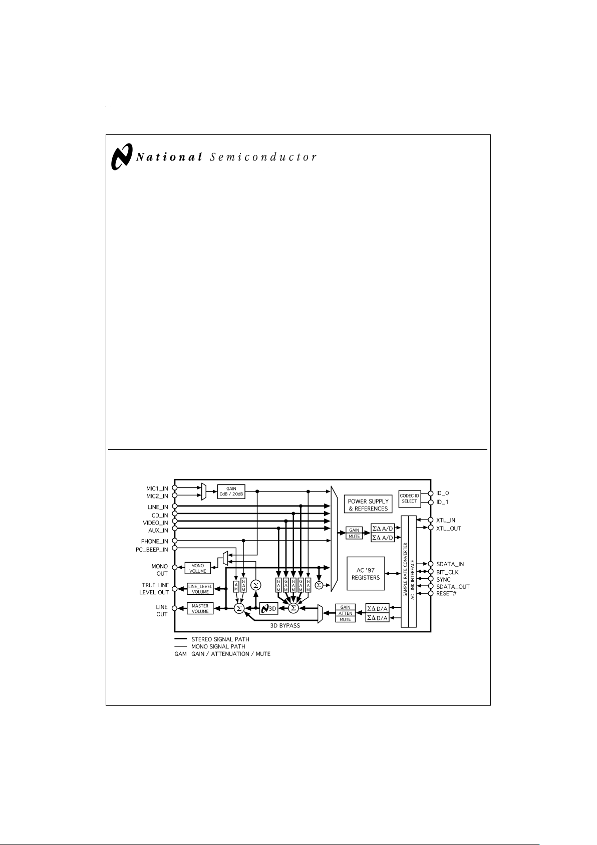
The LM4548 is an audio codec for PC systems which is fully
PC98 compliant and performs the analog intensivefunctions
of the AC97 Rev2 architecture. Using 18-bit Sigma-Delta
A/D’s and D/A’s, the LM4548 provides 90dB of Dynamic
Range.
The LM4548 was designed specifically to provide a high
quality audiopathand provide all analog functionality in a PC
audio system. It features full duplex stereo A/D’s and D/A’s
and an analog mixer with 4 stereo and 3 mono inputs, each
of which has separate gain, attenuation and mute control.
The LM4548 also provides the additional True Line-Level
output and National’s 3D Sound stereo enhancement.
The LM4548 supports variable sample rate conversion as
defined in the AC97 Rev2 specification. The sample rate for
the A/D and D/A can be programmed separately to convert
any rate between 4kHz - 48kHz with a resolution of 1Hz. The
AC97 architecture separates the analog and digital functions
of the PC audio system allowing both for system design flexibility and increased performance.
Key Specifications
n Analog Mixer Dynamic Range 97dB (typ)
n D/A Dynamic Range 89dB (typ)
n A/D Dynamic Range 90dB (typ)
Features
n AC’97 Rev2 compliant
n National’s 3D Sound circuitry
n High quality Sample Rate Conversion (SRC) from 4kHz
to 48kHz in 1Hz increments.
n Multiple Codec Support
n True Line Level Output with volume control in addition to
standard Line Out
n Advanced power management support
n Digital 3V and 5V compliant
Applications
n Desktop PC Audio Systems
n Portable PC Systems
n Mobile PC Systems
Block Diagram
DS100987-1
FIGURE 1. LM4548 Block Diagram
February 1999
LM4548 AC ’97 Rev 2 Codec with Sample Rate Conversion and National 3D Sound
© 1999 National Semiconductor Corporation DS100987 www.national.com
Absolute Maximum Ratings (Note 3)
If Military/Aerospace specified devices are required,
please contact the National Semiconductor Sales Office/
Distributors for availability and specifications.
Supply Voltage 6.0V
Storage Temperature −40˚C to +150˚C
Input Voltage −0.3V to V
DD
+0.3V
ESD Susceptibility (Note 5) 2500V
pins 27, 28 1500V
pin 3 750V
ESD Susceptibility (Note 6) 200V
pin 3 100V
Junction Temperature 150˚C
Soldering Information
TQFP Package
Vapor Phase (60 sec.) 215˚C
Infrared (15 sec.) 220˚C
See AN-450 ″Surface Mounting and their Effects on
Product Reliability″ for other methods of
soldering surface mount devices.
θ
JA
(typ)—VBH48A 74˚C/W
Operating Ratings
Temperature Range
T
MIN
≤ TA≤ T
MAX
−40˚C ≤ TA≤ 85˚C
Analog Supply Range 4.2V ≤ AV
DD
≤ 5.5V
Digital Supply Range 3.0V ≤ DV
DD
≤ 5.5V
Electrical Characteristics (Notes 1, 3)
The following specifications apply for AVDD= 5V, DVDD= 5V, Fs = 48kHz, single codec configuration, unless otherwise noted.
Limits apply for TA= 25˚C. The reference for 0dB is 1Vrms unless otherwise specified.
Symbol Parameter Conditions
LM4548
Units
(Limits)
Typical
(Note 7)
Limit
(Note 8)
AV
DD
Analog Supply Range 4.2 V (min)
5.5 V (max)
DV
DD
Digital Supply Range 3.0 V (min)
5.5 V (max)
D
IDD
Digital Quiescent Power Supply
Current
D
VDD
=5V 43 mA
D
VDD
= 3.3V 20 mA
A
IDD
Analog Quiescent Power Supply
Current
53 mA
I
DSD
Digital Shutdown Current 500 µA
I
ASD
Analog Shutdown Current 30 µA
V
REF
Reference Voltage 2.23 V
PSRR Power Supply Rejection Ratio 40 dB
Analog Loopthru Mode
Dynamic Range (Note 2)
CD Input to Line Output, -60dB Input
THD+N, A-Weighted
97 90 dB (min)
THD Total Harmonic Distortion V
O
= -3dB, f = 1kHz, RL= 10kΩ 0.01 0.02
%
(max)
Analog Input Section
V
IN
Line Input Voltage 1 Vrms
Mic Input with 20dB Gain 0.1 Vrms
Mic Input with 0dB Gain 1 Vrms
Xtalk Crosstalk CD Left to Right -95 dB
Z
IN
Input Impedance(Note 2) 40 10 kΩ (min)
C
IN
Input Capacitance 15 pF
Interchannel Gain Mismatch CD Left to Right 0.01 dB
Record Gain Amplifier - A/D
A
S
Step Size 0dB to 22.5dB 1.5 dB
Mixer Section
A
S
Step Size +12dB to -34.5dB 1.5 dB
A
M
Mute Attenuation 86 dB
Analog to Digital Converters
Resolution 18 Bits
www.national.com 2
Electrical Characteristics (Notes 1, 3) (Continued)
The following specifications apply for AVDD= 5V, DVDD= 5V, Fs = 48kHz, single codec configuration, unless otherwise noted.
Limits apply for TA= 25˚C. The reference for 0dB is 1Vrms unless otherwise specified.
Symbol Parameter Conditions
LM4548
Units
(Limits)
Typical
(Note 7)
Limit
(Note 8)
Analog to Digital Converters
Dynamic Range (Note 2) -60dB Input THD+N, A-Weighted 90 86 dB (min)
Frequency Response -1dB Bandwidth 20 kHz
Digital to Analog Converters
Resolution 18 Bits
Dynamic Range (Note 2) -60dB Input THD+N, A-Weighted 89 85 dB (min)
THD Total Harmonic Distortion V
IN
= -3dB, f=1kHz, RL= 10kΩ 0.01
%
Frequency Response 20 - 21k Hz
Group Delay (Note 2) 2 mS (max)
Out of Band Energy -40 dB
Stop Band Rejection 70 dB
D
T
Discrete Tones -96 dB
True Line Level Output Volume Section
A
S
Step Size 0dB to -46.5dB 1.5 dB
A
M
Mute Attenuation 86 dB
Digital I/O (Note 2)
V
IL
Low level input voltage
0.30 x
DVDD
V (max)
V
HI
High level input voltage
0.40 x
DVDD
V (min)
V
OH
High level output voltage
0.50 x
DVDD
V (min)
V
OL
Low level output voltage
0.20 x
DVDD
V (max)
I
L
Input Leakage Current AC Link inputs
±
10 µA
I
L
Tri state Leakage Current High impedance AC Link outputs
±
10 µA
I
DR
Output drive current AC Link outputs 5 mA
Digital Timing Specifications (Note 2)
F
BC
BIT_CLK frequency 12.288 MHz
T
BCP
BIT_CLK period 81.4 nS
T
CH
BIT_CLK high
Variation of BIT_CLK period from 50
%
duty cycle
±
20
%
(max)
F
SYNC
SYNC frequency 48 kHz
T
SP
SYNC period 20.8 µS
T
SH
SYNC high pulse width 1.3 µS
T
SL
SYNC low pulse width 19.5 µS
T
SETUP
Setup Time
SDATA_IN, SDATA_OUT to falling
edge of BIT_CLK
15 nS (min)
T
HOLD
Hold Time
Hold time of SDATA_IN, SDATA_OUT
from falling edge of BIT_CLK
5 nS (min)
T
RISE
Rise Time
BIT_CLK, SYNC, SDATA_IN or
SDATA_OUT
6 nS (max)
T
FALL
Fall Time
BIT_CLK, SYNC, SDATA_IN or
SDATA_OUT
6 nS (max)
T
RST_LOW
RESET# active low pulse width For cold reset 1.0 µS (min)
T
RST2CLK
RESET# inactive to BIT_CLK start
up
For cold reset 162.8 nS (min)
www.national.com3
Electrical Characteristics (Notes 1, 3) (Continued)
The following specifications apply for AVDD= 5V, DVDD= 5V, Fs = 48kHz, single codec configuration, unless otherwise noted.
Limits apply for TA= 25˚C. The reference for 0dB is 1Vrms unless otherwise specified.
Symbol Parameter Conditions
LM4548
Units
(Limits)
Typical
(Note 7)
Limit
(Note 8)
Digital Timing Specifications (Note 2)
T
SH
SYNC active high pulse width For warm reset 1.3 µS
T
SYNC2CLK
SYNC inactive to BIT_CLK start up For warm reset 162.8 nS (min)
T
SU2RST
Setup to trailing edge of RESET# For ATE Test Mode 15 nS (min)
T
RST2HZ
Rising edge of RESET# to Hi-Z For ATE Test Mode 25 nS (max)
Note 1: All voltages are measured with respect to the ground pin, unless otherwise specified.
Note 2: These specifications are guaranteed by design and characterization; they are not production tested.
Note 3:
Absolute Maximum Ratings
indicate limits beyond which damage to the device may occur.
Operating Ratings
indicate conditions for which the device is func-
tional, but do not guarantee specific performance limits.
Electrical Characteristics
state DC and AC electrical specifications under particular test conditions which guarantee specific performance limits. This assumes that the device is within the Operating Ratings. Specifications are not guaranteed for parameters where no limit is
given, however, the typical value is a good indication of device performance.
Note 4: The maximum power dissipation must be derated at elevated temperatures and is dictated by T
JMAX
, θJA, and the ambient temperature TA. The maximum
allowable power dissipation is P
DMAX
=(T
JMAX–TA
)/θJAor the number given in Absolute Maximum Ratings, whichever is lower. For the LM4548, T
JMAX
= 150˚C. The
typical junction-to-ambient thermal resistance is 74˚C/W for package number VBH48A.
Note 5: Human body model, 100 pF discharged through a 1.5 kΩ resistor.
Note 6: Machine Model, 220 pF–240 pF discharged through all pins.
Note 7: Typicals are measured at 25˚C and represent the parametric norm.
Note 8: Limits are guaranteed to National’s AOQL (Average Outgoing Quality Level).
www.national.com 4
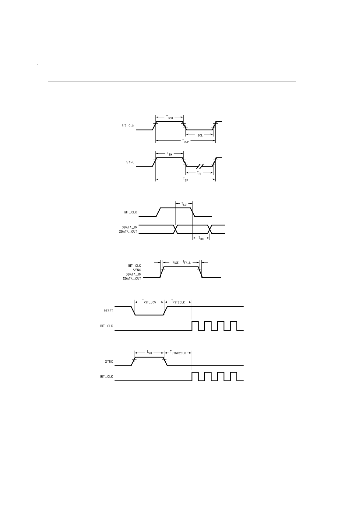
Timing Diagrams
Clocks
DS100987-10
Data Setup and Hold
DS100987-11
Digital Rise and Fall
DS100987-12
Cold Reset
DS100987-13
Warm Reset
DS100987-14
www.national.com5
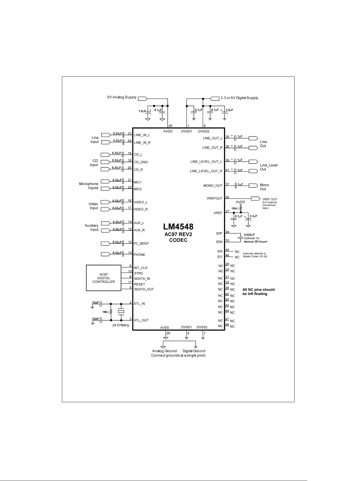
Typical Application
DS100987-3
FIGURE 2. LM4548 Typical Application Circuit
www.national.com 6
 Loading...