NSC LM431CIZ, LM431CIMX, LM431CIM3X, LM431CIM3, LM431BIM3 Datasheet
...
LM431
Adjustable Precision Zener Shunt Regulator
LM431 Adjustable Precision Zener Shunt Regulator
December 1999
General Description
The LM431 is a 3-terminal adjustable shunt regulator with
guaranteed temperature stability over the entire temperature
range of operation. It is now available in a chip sized package (4-Bump micro SMD) using National’s micro SMD package technology. The output voltage may be set at any level
greater than 2.5V (V
external resistors that act as a voltage divided network. Due
to the sharp turn-on characteristics this device is an excellent replacement for many zener diode applications.
) up to 36V merely by selecting two
REF
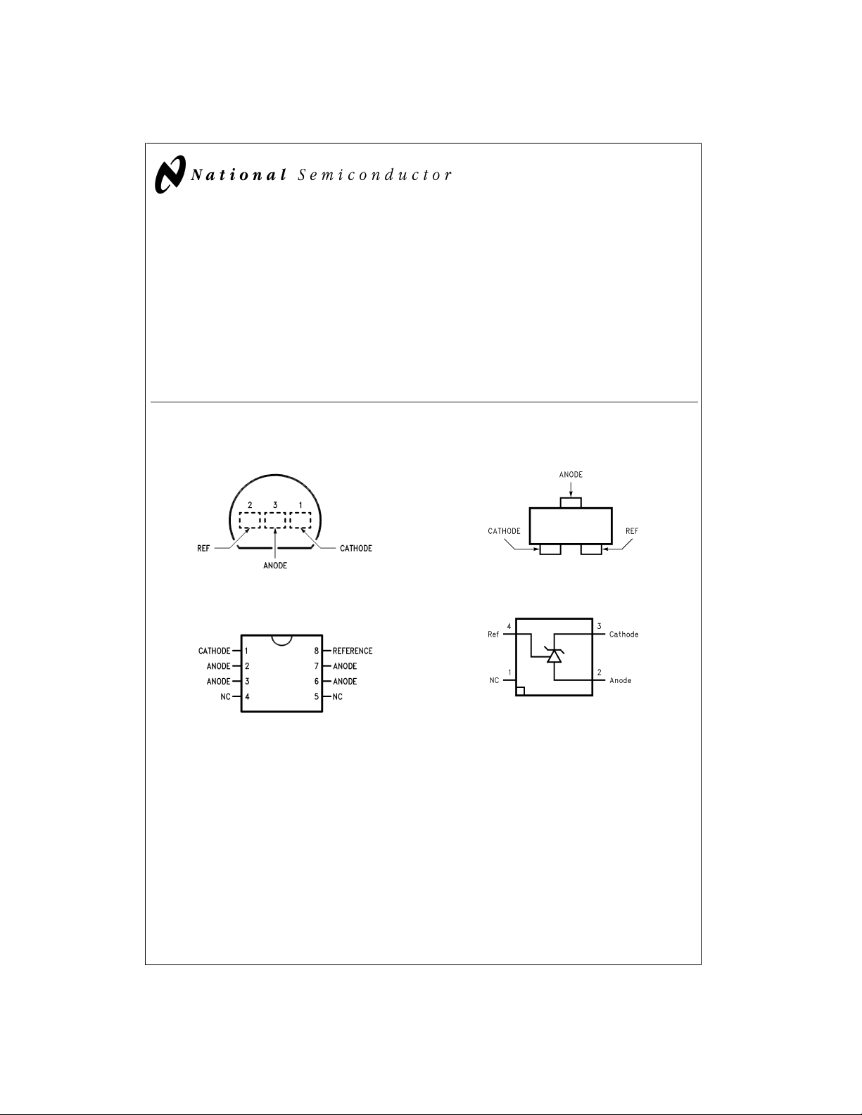
Connection Diagrams
TO-92: Plastic Package
DS010055-1
Top View
SO-8: 8-Pin Surface Mount
Features
n Average temperature coefficient 50 ppm/˚C
n Temperature compensated for operation over the full
temperature range
n Programmable output voltage
n Fast turn-on response
n Low output noise
n LM431 in micro SMD package
SOT-23: 3-Lead Small Outline
DS010055-28
Top View
4-Bump micro SMD
DS010055-54
DS010055-2
Top view
© 1999 National Semiconductor Corporation DS010055 www.national.com
Top View
(bump side down)

Ordering Information
LM431
Package Typical Accuracy Order Number/Package Marking Temperature
%
0.5
TO-92 LM431CCZ/
SO-8 LM431CCM/
SOT-23 LM431CCM3/
micro SMD
Note 1: The micro SMD package marking is a 2 digit manufacturing Date Code only
LM431CCZ
LM431CIZ/
LM431CIZ
431CCM
LM431CIM/
431CIM
N1B
LM431CIM3
N1A
––
%
1
LM431BCZ/
LM431BCZ
LM431BIZ/
LM431BIZ
LM431BCM/
431BCM
LM431BIM/
431BIM
LM431BCM3/
N1D
LM431BIM3
N1C
%
2
LM431ACZ/
LM431ACZ
LM431AIZ/
LM431AIZ
LM431ACM/
LM431ACM
LM431AIM/
LM431AIM
LM431ACM3/
N1F
LM431AIM3
N1E
LM431AIBP
LM431AIBPX(Note 1)
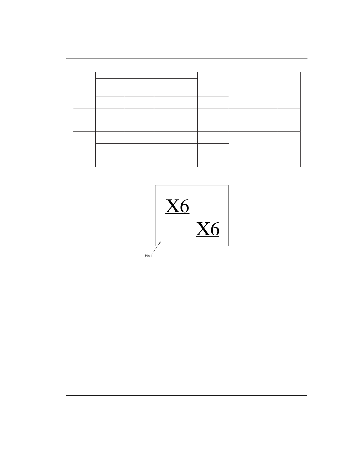
micro SMD Top View Marking Example
Range
0˚C to +70˚C
−40˚C to +85˚C
0˚C to +70˚C
−40˚C to +85˚C
0˚C to +70˚C
−40˚C to +85˚C
−40˚C to +85˚C
Transport Media NSC
Rails Z03A
Rails and Tape &Reel M08A
Rails and Tape &Reel MA03B
250 Units Tape and Reel
3k Units Tape and Reel
Drawing
BPA04AFA
DS010055-56
The LM431 micro SMD Package will be marked with a two digit date manufacturing code. The underline indicates the bottom of
the marking. Pin one will be placed at the bottom left hand corner,and the rest of the pin numbers will follow counter-clockwise.
www.national.com 2

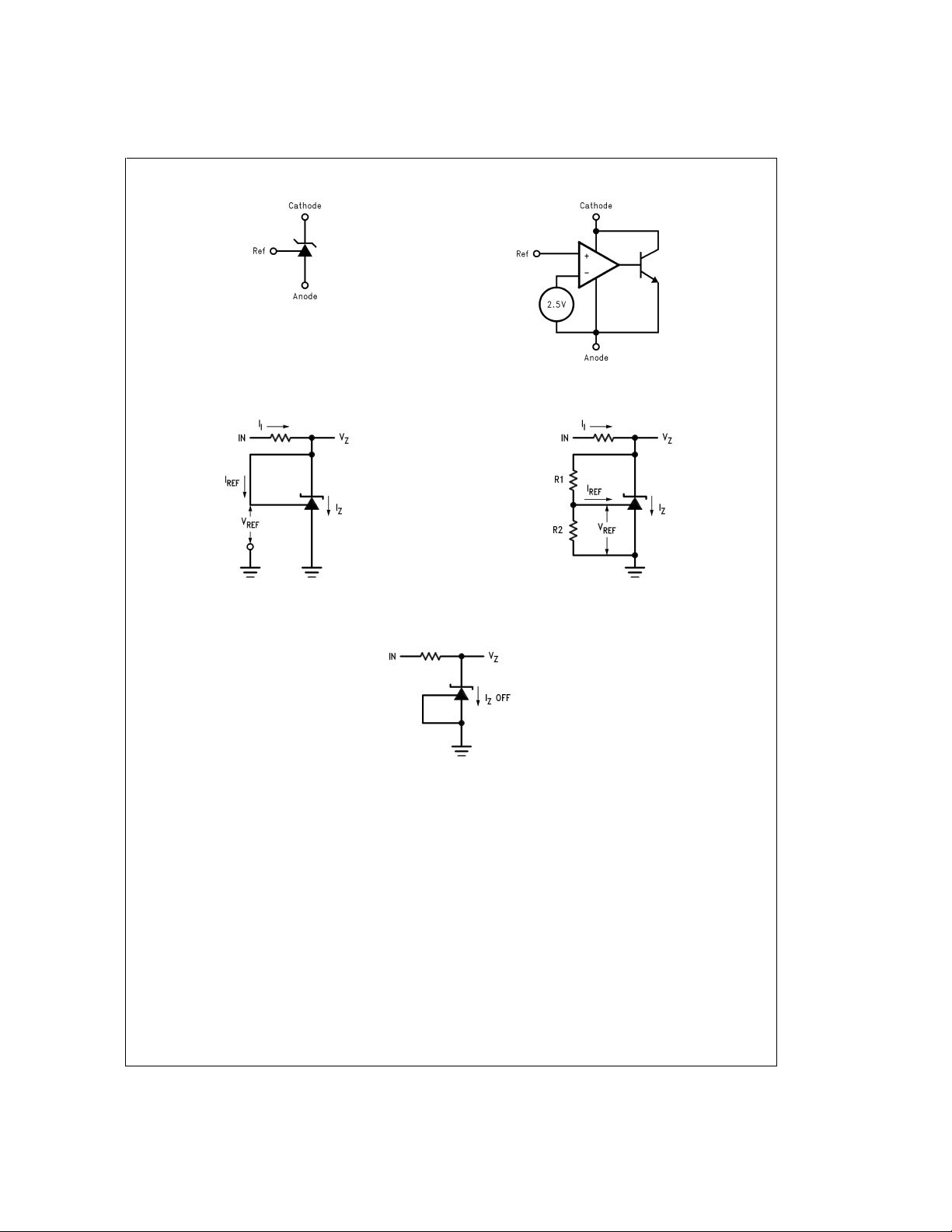
Symbol and Functional Diagrams
DS010055-99
DC Test Circuits
LM431
DS010055-55
DS010055-4
FIGURE 1. Test Circuit for V
=
=
V
Z
REF
Note: V
Z
V
REF
(1 + R1/R2) + I
FIGURE 2. Test Circuit for V
DS010055-6
FIGURE 3. Test Circuit for Off-State Current
REF
•
R1
DS010055-5
>
V
Z
REF
www.national.com3

Absolute Maximum Ratings (Note 2)
LM431
If Military/Aerospace specified devices are required,
please contact the NationalSemiconductorSalesOffice/
Distributors for availability and specifications.
Storage Temperature Range −65˚C to +150˚C
Operating Temperature Range
Reference Voltage −0.5V
Reference Input Current 10 mA
Internal Power Dissipation (Notes 3, 4)
TO-92 Package
SO-8 Package
SOT-23 Package
micro SMD Package 0.30W
Industrial (LM431xI) −40˚C to +85˚C
Commercial (LM431xC) 0˚C to +70˚C
Soldering Information
Infrared or Convection (20 sec.) 235˚C
Wave Soldering (10 sec.) 260˚C (lead temp.)
Cathode Voltage 37V
Operating Conditions
Cathode Voltage V
Cathode Current 1.0 mA 100 mA
Min Max
REF
Continuous Cathode Current −10 mA to +150 mA
LM431
Electrical Characteristics
=
T
25˚C unless otherwise specified
A
Symbol Parameter Conditions Min Typ Max Units
V
REF
Reference Voltage V
=
Z
LM431A
=
V
Z
LM431B
=
V
Z
LM431C
V
DEV
I
REF
∝
I
I
Z(MIN)
I
Z(OFF)
r
Z
REF
Deviation of Reference Input Voltage Over V
Temperature (Note 5) T
Ratio of the Change in Reference Voltage I
to the Change in Cathode Voltage
Reference Input Current R
Deviation of Reference Input Current over R
Temperature I
Minimum Cathode Current for Regulation V
Off-State Current V
Dynamic Output Impedance (Note 6) V
=
Z
=
A
=
Z
(Figure 2 )
=
1
=
I
10 mA
I
=
1
=
10 mA, 0.4 1.2 µA
I
=
T
A
=
Z
=
Z
=
Z
Frequency=0Hz
=
V
Z
Frequency=0Hz
Note 2: Absolute Maximum Ratings indicate limits beyond which damage to the device may occur. Electrical specifications do not apply when operating the device
beyond its rated operating conditions.
Note 3: T
Note 4: Ratings apply to ambient temperature at 25˚C. Above this temperature, derate the TO-92 at 6.2 mW/˚C, the SO-8 at 6.5 mW/˚C, the SOT-23 at 2.2 mW/˚C
and the micro SMD at 3mW/˚C.
Note 5: Deviation of reference input voltage, V
J Max
=
150˚C.
, is defined as the maximum variation of the reference input voltage over the full temperature range.
DEV
=
V
10 mA 2.440 2.495 2.550 V
REF,II
(Figure 1 )
=
V
10 mA 2.470 2.495 2.520 V
REF,II
(Figure 1 )
=
V
10 mA 2.485 2.500 2.510 V
REF,II
(Figure 1 )
=
V
Full Range
10 mA V
10 mA, 8.0 17 mV
REF,II
(Figure 1 )
from V
Z
to 10V −1.4 −2.7
REF
VZfrom 10V to 36V −1.0 −2.0
=
∞
10 kΩ,R
, 2.0 4.0 µA
2
(Figure 2 )
=
∞
2
(Figure 2 )
(Figure 1 )
=
0V
REF
,
(Figure 3 )
0.4 1.0 mA
0.3 1.0 µA
10 kΩ,R
Full Range
V
REF
36V, V
, LM431A, 0.75 Ω
V
REF
(Figure 1 )
, LM431B, LM431C 0.50 Ω
V
REF
(Figure 1 )
37V
0.78W
0.81W
0.28W
mV/V
www.national.com 4
 Loading...