

NSC LM4250CN, LM4250CMX, LM4250CMWC, LM4250CM, LM4250CH Datasheet
...
LM4250
Programmable Operational Amplifier
General Description
The LM4250 and LM4250C are extremely versatile programmable monolithic operational amplifiers. A single external
master bias current setting resistor programs the input bias
current, input offset current, quiescent power consumption,
slew rate, input noise, and the gain-bandwidth product. The
device is a truly general purpose operational amplifier.
The LM4250C is identical to the LM4250 except that the
LM4250C has its performance guaranteed over a 0˚C to
+70˚C temperature range instead of the −55˚C to +125˚C
temperature range of the LM4250.
Features
n
±
1V to±18V power supply operation
n 3 nA input offset current
n Standby power consumption as low as 500 nW
n No frequency compensation required
n Programmable electrical characteristics
n Offset voltage nulling capability
n Can be powered by two flashlight batteries
n Short circuit protection
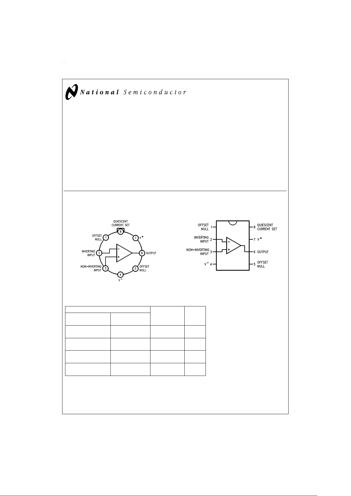
Connection Diagrams
Ordering Information
Temperature Range Package NSC
Military Commercial Package
−55˚C ≤ T
A
≤ +125˚C 0˚C ≤ TA≤ +70˚C Number
LM4250CN 8-Pin N08E
Molded DIP
LM4250CM 8-Pin M08A
Surface Mount
LM4250J 8-Pin J08E
LM4250J-MIL Ceramic DIP
LM4250H LM4250CH 8-Pin H08C
LM4250H-MIL Metal Can
Metal Can Package
DS009300-2
Top View
Dual-In-Line Package
DS009300-5
Top View
May 1998
LM4250 Programmable Operational Amplifier
© 1999 National Semiconductor Corporation DS009300 www.national.com

Absolute Maximum Ratings (Note 1)
If Military/Aerospace specified devices are required,
please contact the National Semiconductor Sales Office/
Distributors for availability and specifications.
(Note 3)
LM4250 LM4250C
Supply Voltage
±
18V
±
18V
Operating Temp. Range −55˚C ≤ T
A
≤ +125˚C 0˚C ≤ TA≤ +70˚C
Differential Input Voltage
±
30V
±
30V
Input Voltage (Note 2)
±
15V
±
15V
I
SET
Current 150 nA 150 nA
Output Short Circuit Duration Continuous Continuous
T
JMAX
H-Package 150˚C 100˚C
N-Package 100˚C
J-Package 150˚C 100˚C
M-Package 100˚C
Power Dissipation at T
A
=
25˚C
H-Package (Still Air) 500 mW 300 mW
(400 LF/Min Air Flow) 1200 mW 1200 mW
N-Package 500 mW
J-Package 1000 mW 600 mW
M-Package 350 mW
Thermal Resistance (Typical) θ
JA
H-Package (Still Air) 165˚C/W 165˚C/W
(400 LF/Min Air Flow) 65˚C/W 65˚C/W
N-Package 130˚C/W
J-Package 108˚C/W 108˚C/W
M-Package 190˚C/W
(Typical) θ
JC
H-Package 21˚C/W 21˚C/W
Storage Temperature Range −65˚C to +150˚C −65˚C to +150˚C
Soldering Information
Dual-In-Line Package
Soldering (10 seconds) 260˚C
Small Outline Package
Vapor Phase (60 seconds) 215˚C
Infrared (15 seconds) 220˚C
See AN-450 “Surface Mounting Methods and Their Effect
on Product Reliability” for other methods of soldering
surface mount devices.
ESD tolerance (Note 4) 800V
Note 1: “Absolute Maximum Ratings” indicate limits beyond which damage
to the device may occur. Operating Ratings indicate conditionsforwhichthe
device is functional, but do not guarantee specific performance limits.
Note 2: For supply voltages less than
±
15V, the absolute maximum input
voltage is equal to the supply voltage.
Note 3: Refer to RETS4250X for military specifications.
Note 4: Human body model, 1.5 kΩ in series with 100 pF.
www.national.com 2
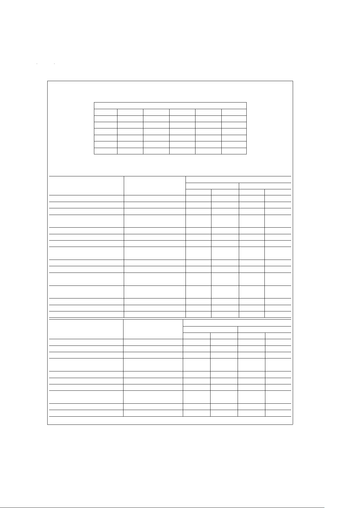
Resistor Biasing
Set Current Setting Resistor to V
−
I
SET
V
S
0.1 µA 0.5 µA 1.0 µA 5 µA 10 µA
±
1.5V 25.6 MΩ 5.04 MΩ 2.5 MΩ 492 kΩ 244 kΩ
±
3.0V 55.6 MΩ 11.0 MΩ 5.5 MΩ 1.09 MΩ 544 kΩ
±
6.0V 116 MΩ 23.0 MΩ 11.5 MΩ 2.29 MΩ 1.14 MΩ
±
9.0V 176 MΩ 35.0 MΩ 17.5 MΩ 3.49 MΩ 1.74 MΩ
±
12.0V 236 MΩ 47.0 MΩ 23.5 MΩ 4.69 MΩ 2.34 MΩ
±
15.0V 296 MΩ 59.0 MΩ 29.5 MΩ 5.89 MΩ 2.94 MΩ
Electrical Characteristics
LM4250 (−55˚C ≤ TA≤ +125˚C unless otherwise specified.) T
A
=
T
J
V
S
=
±
1.5V
Parameter Conditions I
SET
=
1µA I
SET
=
10 µA
Min Max Min Max
V
OS
RS≤ 100 kΩ,T
A
=
25˚C 3 mV 5 mV
I
OS
T
A
=
25˚C 3 nA 10 nA
I
bias
T
A
=
25˚C 7.5 nA 50 nA
Large Signal Voltage R
L
=
100 kΩ,T
A
=
25˚C 40k
Gain V
O
=
±
0.6V, R
L
=
10 kΩ 50k
Supply Current T
A
=
25˚C 7.5 µA 80 µA
Power Consumption T
A
=
25˚C 23 µW 240 µW
V
OS
RS≤ 100 kΩ 4mV 6mV
I
OS
T
A
=
+125˚C 5 nA 10 nA
T
A
=
−55˚C 3 nA 10 nA
I
bias
7.5 nA 50 nA
Input Voltage Range
±
0.6V
±
0.6V
Large Signal Voltage Gain V
O
=
±
0.5V, R
L
=
100 kΩ 30k
R
L
=
10 kΩ 30k
Output Voltage Swing R
L
=
100 kΩ
±
0.6V
R
L
=
10 kΩ
±
0.6V
Common Mode Rejection Ratio R
S
≤ 10 kΩ 70 dB 70 dB
Supply Voltage Rejection Ratio R
S
≤ 10 kΩ 76 dB 76 dB
Supply Current 8µA 90µA
V
S
=
±
15V
Parameter Conditions I
SET
=
1µA I
SET
=
10 µA
Min Max Min Max
V
OS
RS≤ 100 kΩ,T
A
=
25˚C 3 mV 5 mV
I
OS
T
A
=
25˚C 3 nA 10 nA
I
bias
T
A
=
25˚C 7.5 nA 50 nA
Large Signal Voltage R
L
=
100 kΩ,T
A
=
25˚C 100k
Gain V
O
=
±
10V, R
L
=
10 kΩ 100k
Supply Current T
A
=
25˚C 10 µA 90 µA
Power Consumption T
A
=
25˚C 300 µW 2.7 mW
V
OS
RS≤ 100 kΩ 4mV 6mV
I
OS
T
A
=
+125˚C 25 nA 25 nA
T
A
=
−55˚C 3 nA 10 nA
I
bias
7.5 nA 50 nA
Input Voltage Range
±
13.5V
±
13.5V
www.national.com3
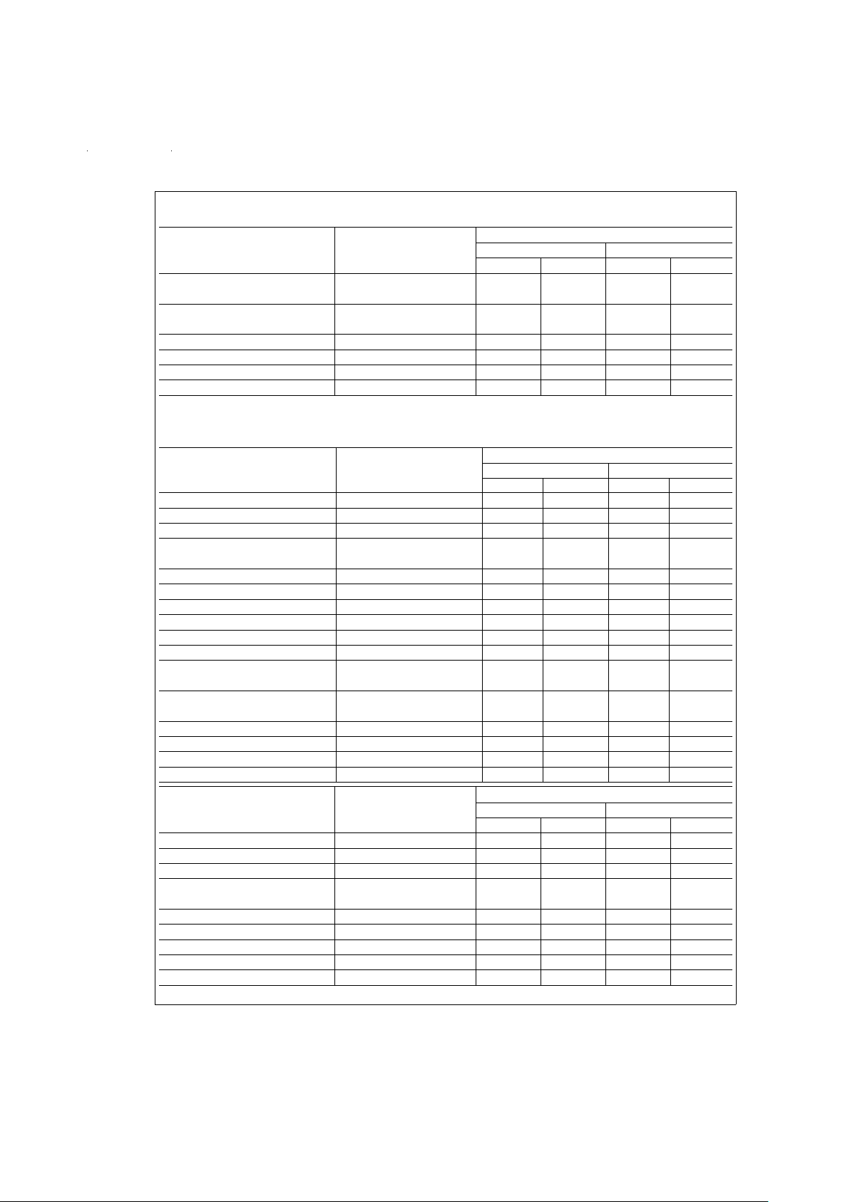
Electrical Characteristics (Continued)
V
S
=
±
15V
Parameter Conditions I
SET
=
1µA I
SET
=
10 µA
Min Max Min Max
Large Signal Voltage V
O
=
±
10V, R
L
=
100 kΩ 50k
Gain R
L
=
10 kΩ 50k
Output Voltage Swing R
L
=
100 kΩ
±
12V
R
L
=
10 kΩ
±
12V
Common Mode Rejection Ratio R
S
≤ 10 kΩ 70 dB 70 dB
Supply Voltage Rejection Ratio R
S
≤ 10 kΩ 76 dB 76 dB
Supply Current 11 µA 100 µA
Power Consumption 330 µW 3 mW
Electrical Characteristics
LM4250C (0˚C ≤ TA≤ +70˚C unless otherwise specified.) T
A
=
T
J
V
S
=
±
1.5V
Parameter Conditions I
SET
=
1µA I
SET
=
10 µA
Min Max Min Max
V
OS
RS≤ 100 kΩ,T
A
=
25˚C 5 mV 6 mV
I
OS
T
A
=
25˚C 6 nA 20 nA
I
bias
T
A
=
25˚C 10 nA 75 nA
Large Signal Voltage Gain R
L
=
100 kΩ,T
A
=
25˚C 25k
V
O
=
±
0.6V, R
L
=
10 kΩ 25k
Supply Current T
A
=
25˚C 8 µA 90 µA
Power Consumption T
A
=
25˚C 24 µW 270 µW
V
OS
RS≤ 10 kΩ 6.5 mV 7.5 mV
I
OS
8nA 25nA
I
bias
10 nA 80 nA
Input Voltage Range
±
0.6V
±
0.6V
Large Signal Voltage V
O
=
±
0.5V, R
L
=
100 kΩ 25k
Gain R
L
=
10 kΩ 25k
Output Voltage Swing R
L
=
100 kΩ
±
0.6V
R
L
=
10 kΩ
±
0.6V
Common Mode Rejection Ratio R
S
≤ 10 kΩ 70 dB 70 dB
Supply Voltage Rejection Ratio R
S
≤ 10 kΩ 74 dB 74 dB
Supply Current 8µA 90µA
Power Consumption 24 µW 270 µW
V
S
=
±
15V
Parameter Conditions I
SET
=
1µA I
SET
=
10 µA
Min Max Min Max
V
OS
RS≤ 100 kΩ,T
A
=
25˚C 5 mV 6 mV
I
OS
T
A
=
25˚C 6 nA 20 nA
I
bias
T
A
=
25˚C 10 nA 75 nA
Large Signal Voltage R
L
=
100 kΩ,T
A
=
25˚C 60k
Gain V
O
=
±
10V, R
L
=
10 kΩ 60k
Supply Current T
A
=
25˚C 11 µA 100 µA
Power Consumption T
A
=
25˚C 330 µW 3 mW
V
OS
RS≤ 100 kΩ 6.5 mV 7.5 mV
I
OS
8nA 25nA
I
bias
10 nA 80 nA
www.national.com 4
 Loading...