

NSC LM395T, LM195K-883, LM195H-883 Datasheet
LM195/LM395
Ultra Reliable Power Transistors
General Description
The LM195/LM395 are fast, monolithic power transistors
with complete overload protection. These devices, which act
as high gain power transistors, have included on the chip,
current limiting, power limiting, and thermal overload protection making them virtually impossible to destroy from any
type ofoverload.In the standard TO-3transistor power package, the LM195 will deliver load currents in excess of 1.0A
and can switch 40V in 500 ns.
The inclusion of thermal limiting, a feature not easily available in discrete designs, provides virtually absolute protection against overload. Excessive power dissipation or inadequate heat sinking causes the thermal limiting circuitry to
turn off the device preventing excessive heating.
The LM195 offers a significant increase in reliability as well
as simplifying power circuitry. In some applications, where
protection is unusually difficult, such as switching regulators,
lamp or solenoid drivers where normal power dissipation is
low, the LM195 is especially advantageous.
The LM195 is easy to use and only a few precautions need
be observed. Excessive collector to emitter voltage can destroy the LM195 as with any power transistor. When the device is used as an emitter follower with low source imped-
ance, it is necessary to insert a 5.0k resistor in series with
the base lead to prevent possible emitter follower oscillations. Although the device is usually stable as an emitter follower,the resistor eliminates the possibility of trouble without
degrading performance. Finally, since it has good high frequency response, supply bypassing is recommended.
For low-power applications (under 100 mA), refer to the
LP395 Ultra Reliable Power Transistor.
The LM195/LM395 are available in standard TO-3 power
packages and solid Kovar TO-5. The LM195 is rated for operation from −55˚C to +150˚C and the LM395 from 0˚C to
+125˚C.
Features
n Internal thermal limiting
n Greater than 1.0A output current
n 3.0 µA typical base current
n 500 ns switching time
n 2.0V saturation
n Base can be driven up to 40V without damage
n Directly interfaces with CMOS or TTL
n 100%electrical burn-in
LM195/LM395 Ultra Reliable Power Transistors
June 1999
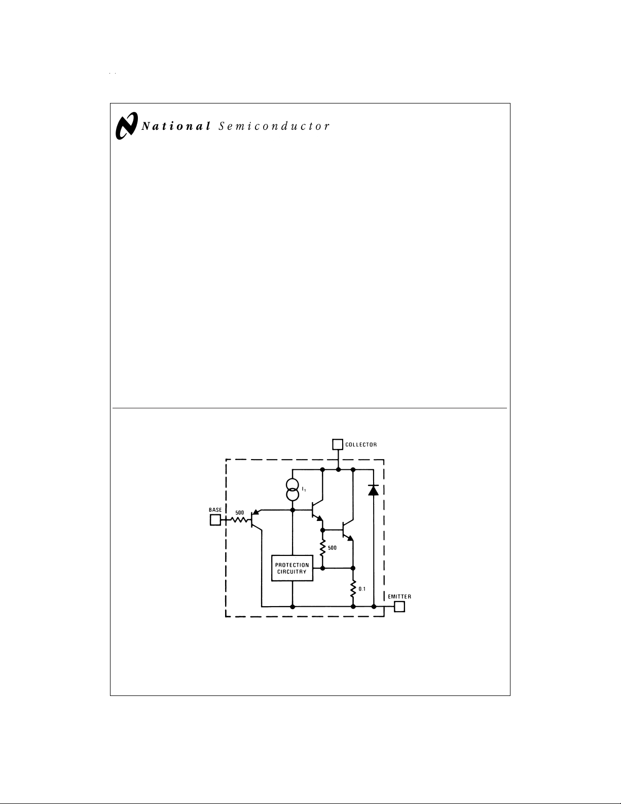
Simplified Circuit
DS006009-1
© 1999 National Semiconductor Corporation DS006009 www.national.com
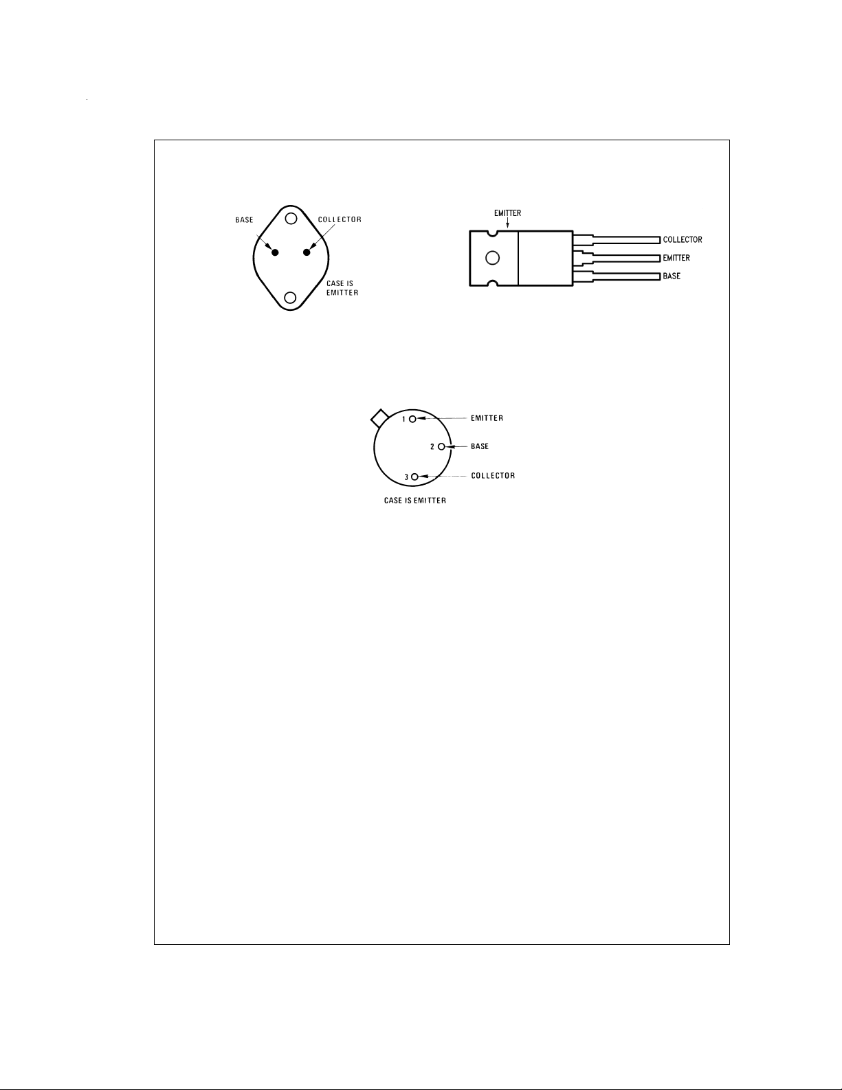
Connection Diagrams
TO-3 Metal Can Package
DS006009-2
Bottom View
Order Number LM195K/883
See NS Package Number K02A
TO-220 Plastic Package
DS006009-3
Case is Emitter
Top View
Order Number LM395T
See NS Package Number T03B
TO-5 Metal Can Package
DS006009-4
Bottom View
Order Number LM195H/883
See NS Package Number H03B
www.national.com 2
Absolute Maximum Ratings (Note 1)
If Military/Aerospace specified devices are required,
please contact the National Semiconductor Sales Office/
Distributors for availability and specifications.
Collector to Emitter Voltage
LM195 42V
LM395 36V
Collector to Base Voltage
LM195 42V
Base to Emitter Voltage (Reverse) 20V
Collector Current Internally Limited
Power Dissipation Internally Limited
Operating Temperature Range
LM195 −55˚C to +150˚C
LM395 0˚C to +125˚C
Storage Temperature Range −65˚C to +150˚C
Lead Temperature
(Soldering, 10 sec.) 260˚C
LM395 36V
Base to Emitter Voltage (Forward)
LM195
LM395
42V
36V
Preconditioning
100%Burn-In In Thermal Limit
Electrical Characteristics
(Note 2)
Parameter Conditions LM195 LM395 Units
Min Typ Max Min Typ Max
Collector-Emitter Operating Voltage I
≤ IC≤ I
Q
MAX
(Note 4)
Base to Emitter Breakdown Voltage 0 ≤ V
≤ V
CE
CEMAX
42 36 60 V
Collector Current
TO-3, TO-220 V
TO-5 V
Saturation Voltage I
Base Current 0 ≤ I
Quiescent Current (IQ)V
Base to Emitter Voltage I
Switching Time V
≤ 15V 1.2 2.2 1.0 2.2 A
CE
≤ 7.0V 1.2 1.8 1.0 1.8 A
CE
≤ 1.0A, T
C
0 ≤ V
be
0 ≤ V
=
C
CE
=
T
A
=
≤ I
C
MAX
≤ V
CE
0
≤ V
CE
1.0A, T
=
36V, R
25˚C
=
25˚C 1.8 2.0 1.8 2.2 V
A
CEMAX
CEMAX
=
+25˚C 0.9 0.9 V
A
=
36Ω,
L
Thermal Resistance Junction to TO-3 Package (K) 2.3 3.0 2.3 3.0 ˚C/W
Case (Note 3) TO-5 Package (H) 12 15 12 15 ˚C/W
TO-220 Package (T) 4 6 ˚C/W
Note 1: “Absolute Maximum Ratings” indicate limits beyond which damage to the device may occur. Operating Ratings indicate conditions for which the device is
functional, but do not guarantee specific performance limits.
Note 2: Unless otherwise specified, these specifications apply for −55˚C ≤ T
Note 3: Without a heat sink, the thermal resistance of the TO-5 package is about +150˚C/W, while that of the TO-3 package is +35˚C/W.
Note 4: Selected devices with higher breakdown available.
Note 5: Refer to RETS195H and RETS195K drawings of military LM195H and LM195K versions for specifications.
≤ +150˚C for the LM195 and 0˚C ≤ +125˚C for the LM395.
j
42 36 V
3.0 5.0 3.0 10 µA
2.0 5.0 2.0 10 mA
500 500 ns
www.national.com3
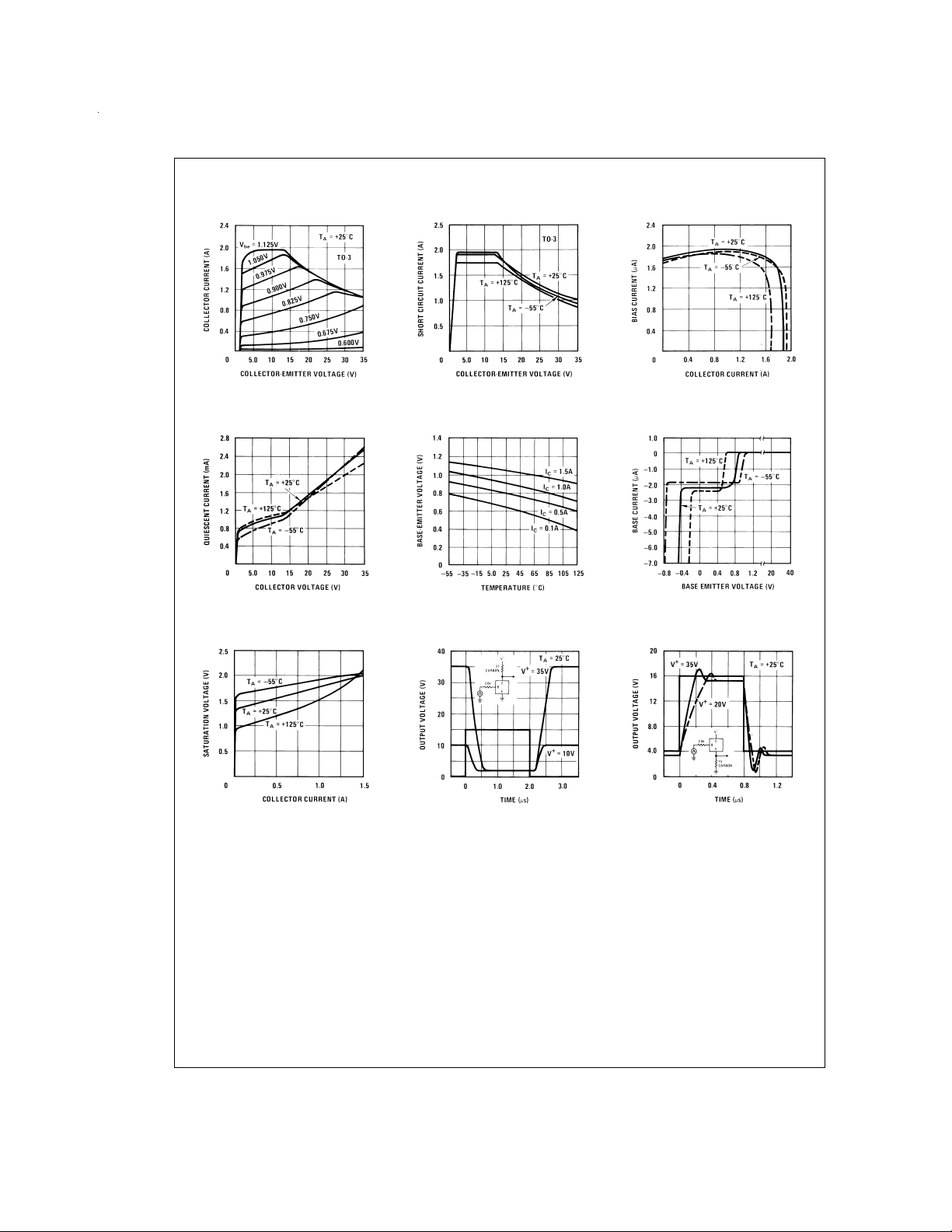
Typical Performance Characteristics (for K and T Packages)
Collector Characteristics
Quiescent Current
Saturation Voltage
DS006009-33
DS006009-36
Short Circuit Current
Base Emitter Voltage
Response Time
DS006009-34
DS006009-37
Bias Current
DS006009-35
Base Current
DS006009-38
Response Time
DS006009-39
www.national.com 4
DS006009-40
DS006009-41
 Loading...