LM3940
1A Low Dropout Regulator for 5V to 3.3V Conversion
General Description
The LM3940 is a 1A low dropout regulator designed to provide 3.3V from a 5V supply.
The LM3940 is ideally suited for systems which contain both
5V and 3.3V logic, with prime power provided from a 5V bus.
Because the LM3940 is a true low dropout regulator, it can
hold its 3.3V output in regulation with input voltages as low
as 4.5V.
The T0-220 package of the LM3940 means that in most applications the full 1A of load current can be delivered without
using an additional heatsink.
The surface mount TO-263 package uses minimum board
space, and gives excellent power dissipation capability when
soldered to a copper plane on the PC board.
Features
n Output voltage specified over temperature
n Excellent load regulation
n Guaranteed 1A output current
n Requires only one external component
n Built-in protection against excess temperature
n Short circuit protected
Applications
n Laptop/Desktop Computers
n Logic Systems
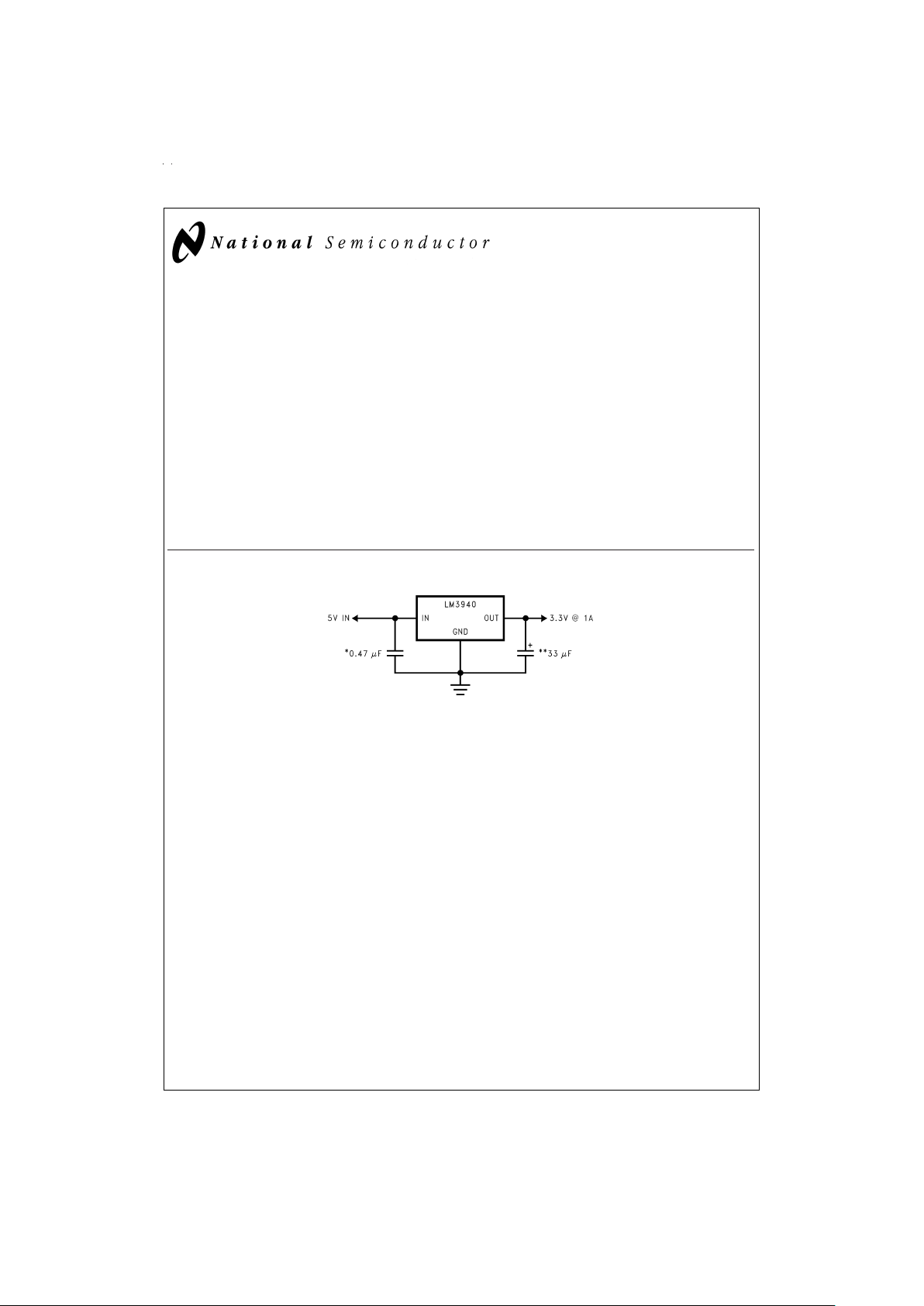
Typical Application
DS012080-1
*
Required if regulator is located more than 1" from the power supply filter capacitor or if battery power is used.
**
See Application Hints.
May 1999
LM3940 1A Low Dropout Regulator for 5V to 3.3V Conversion
© 1999 National Semiconductor Corporation DS012080 www.national.com

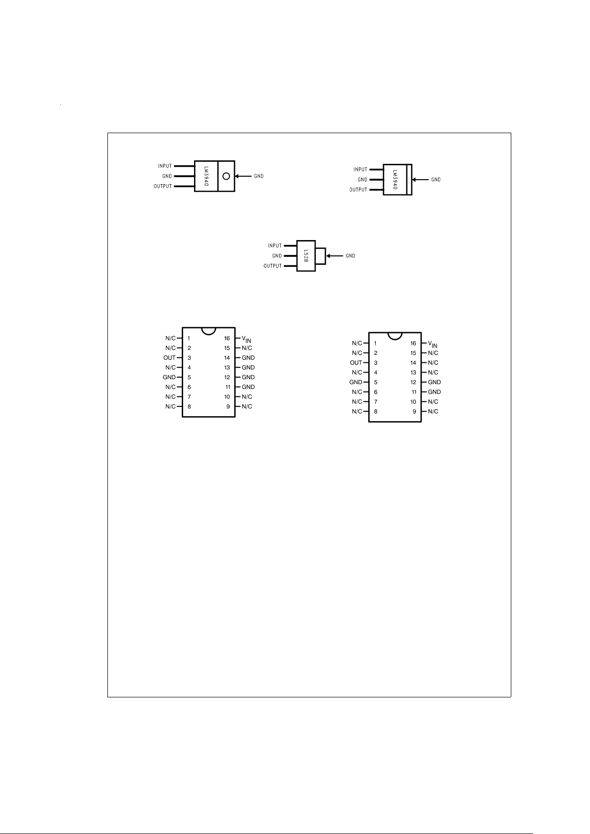
Connection Diagram/Ordering Information
DS012080-2
3-Lead TO-220 Package
(Front View)
Order Part Number LM3940IT-3.3
NSC Drawing Number TO3B
DS012080-3
3-Lead TO-263 Package
(Front View)
Order Part Number LM3940IS-3.3
NSC Drawing Number TS3B
DS012080-10
3-Lead SOT-223
(Front View)
Order Part Number LM3940IMP-3.3
Package Marked L52B
NSC Drawing Number MA04A
DS012080-27
16-Lead Ceramic Dual-in-Line Package
(Top View)
Order Part Number LM3940J-3.3-QML
5962-9688401QEA
NSC Drawing Number J16A
DS012080-28
16-Lead Ceramic Surface-Mount Package
(Top View)
Order Part Number LM3940WG-3.3-QML
5962-9688401QXA
NSC Drawing Number WG16A
www.national.com 2

Absolute Maximum Ratings (Note 1)
If Military/Aerospace specified devices are required,
please contact the National Semiconductor Sales Office/
Distributors for availability and specifications.
Storage Temperature Range −65˚C to +150˚C
Operating Junction Temperature Range −40˚C to +125˚C
Lead Temperature (Soldering, 5 seconds) 260˚C
Power Dissipation (Note 2) Internally Limited
Input Supply Voltage 7.5V
ESD Rating (Note 3) 2 kV
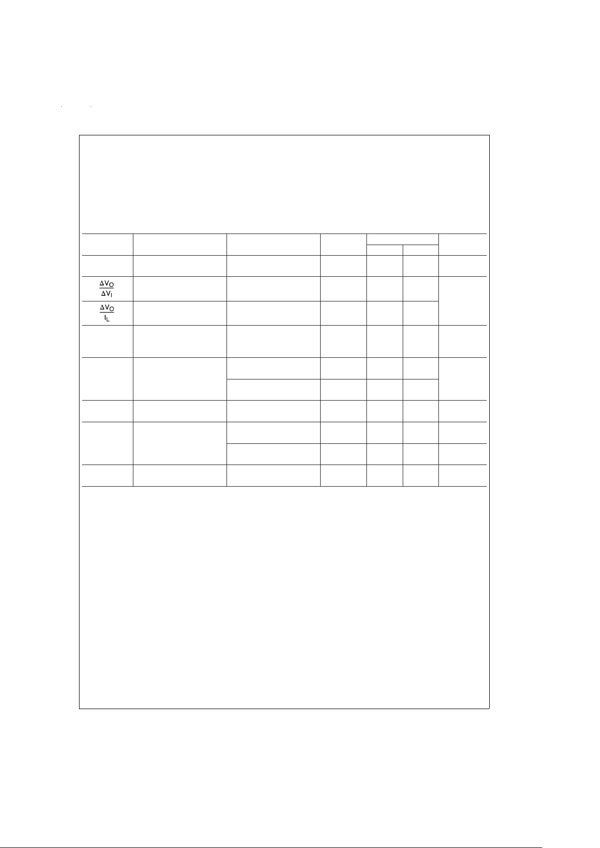
Electrical Characteristics
Limits in standard typeface are for T
J
=
25˚C, and limits in boldface type apply over the full operating temperature range. Un-
less otherwise specified: V
IN
=
5V, I
L
=
1A, C
OUT
=
33 µF.
Symbol Parameter Conditions Typical LM3940 (Note 4) Units
min max
V
O
Output Voltage 5 mA ≤ IL≤ 1A 3.3 3.20 3.40 V
3.13 3.47
Line Regulation I
L
=
5mA
20
40 mV
4.5V ≤ V
O
≤ 5.5V
Load Regulation 50 mA ≤ IL≤ 1A
35
50
80
Z
O
Output Impedance IL(DC)=100 mA
I
L
(AC)=20 mA (rms) 35 mΩ
f=120 Hz
I
Q
Quiescent Current 4.5V ≤ VIN≤ 5.5V 10 15 mA
I
L
=
5mA 20
V
IN
=
5V 110 200
I
L
=
1A 250
e
n
Output Noise Voltage BW=10 Hz–100 kHz 150 µV (rms)
I
L
=
5mA
V
O−VIN
Dropout Voltage I
L
=
1A 0.5 0.8 V
(Note 5) 1.0
I
L
=
100 mA 110 150 mV
200
I
L
(SC) Short Circuit Current R
L
=
0 1.7 1.2 A
Note 1: Absolute maximum ratings indicate limits beyond which damage to the component may occur. Electrical specifications do not apply when operating the device outside of its rated operating conditions.
Note 2: The maximum allowable power dissipation is a function of the maximum junction temperature, T
J
, the junction-to-ambient thermal resistance, θ
J−A
, and the
ambient temperature,T
A
. Exceeding themaximumallowablepower dissipation will cause excessive die temperature, and the regulator will go into thermal shutdown.
The value of θ
J−A
(for devices in still air with no heatsink) is 60˚C/W for the TO-220 package, 80˚C/W for the TO-263 package, and 174˚C/W for the SOT-223 package.
The effective value of θ
J−A
can be reduced by using a heatsink (see Application Hints for specific information on heatsinking).
Note 3: ESD rating is based on the human body model: 100 pF discharged through 1.5 kΩ.
Note 4: All limits guaranteed for T
J
=
25˚C are 100%tested and are used to calculate Outgoing Quality Levels. All limits at temperature extremes are guaranteed
via correlation using standard Statistical Quality Control (SQC) methods.
Note 5: Dropout voltage is defined as the input-output differential voltage where the regulator output drops to a value that is 100 mV below the value that is measured
at V
IN
=
5V.
www.national.com3

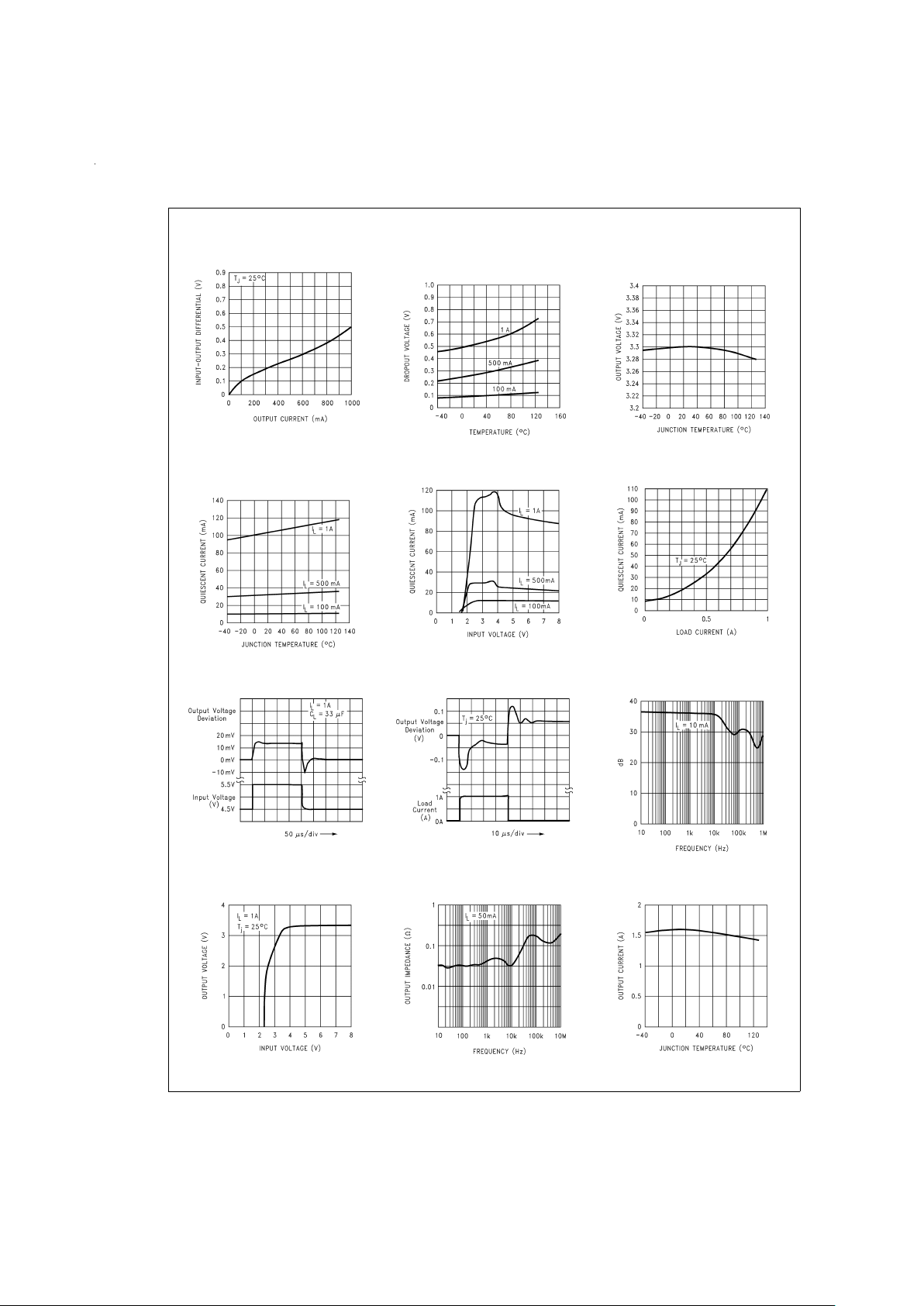
Typical Performance Characteristics
Dropout Voltage
DS012080-13
Dropout Voltage
vs Temperature
DS012080-14
Output Voltage
vs Temperature
DS012080-15
Quiescent Current
vs Temperature
DS012080-16
Quiescent Current vs V
IN
DS012080-17
Quiescent Current vs Load
DS012080-18
Line Transient Response
DS012080-19
Load Transient Response
DS012080-20
Ripple Rejection
DS012080-21
Low Voltage Behavior
DS012080-22
Output Impedance
DS012080-23
Peak Output Current
DS012080-24
www.national.com 4
 Loading...