

July 1992
LM392/LM2924
Low Power Operational Amplifier/Voltage Comparator
LM392/LM2924 Low Power Operational Amplifier/Voltage Comparator
General Description
The LM392 series consists of 2 independent building block
circuits. One is a high gain, internally frequency compensated operational amplifier, and the other is a precision voltage
comparator. Both the operational amplifier and the voltage
comparator have been specifically designed to operate from
a single power supply over a wide range of voltages. Both
circuits have input stages which will common-mode input
down to ground when operating from a single power supply.
Operation from split power supplies is also possible and the
low power supply current is independent of the magnitude
of the supply voltage.
Application areas include transducer amplifier with pulse
shaper, DC gain block with level detector, VCO, as well as
all conventional operational amplifier or voltage comparator
circuits. Both circuits can be operated directly from the standard 5 V
and the output of the comparator will interface directly with
power supply voltage used in digital systems,
DC
either TTL or CMOS logic. In addition, the low power drain
makes the LM392 extremely useful in the design of portable
equipment.
Advantages
Y
Eliminates need for dual power supplies
Y
An internally compensated op amp and a precision
comparator in the same package
Y
Allows sensing at or near ground
Y
Power drain suitable for battery operation
Y
Pin-out is the same as both the LM358 dual op amp
and the LM393 dual comparator
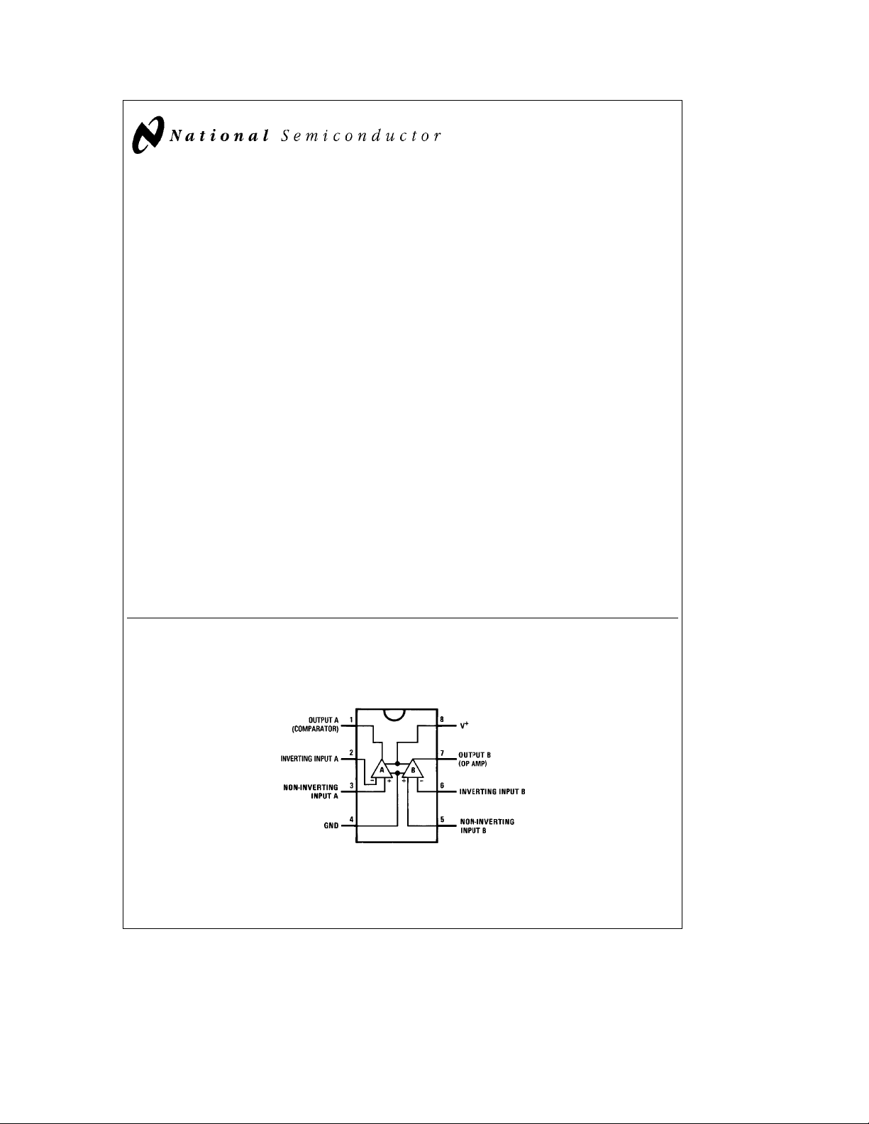
Connection Diagram (Top View)
(Amplifier A
(Amplifier B
e
Dual-In-Line Package
Features
Y
Wide power supply voltage range
Single supply 3V to 32V
Dual supply
Y
Low supply current drainÐessentially independent of
supply voltage 600 mA
Y
Low input biasing current 50 nA
Y
Low input offset voltage 2 mV
Y
Low input offset current 5 nA
Y
Input common-mode voltage range includes ground
Y
Differential input voltage range equal to the power sup-
ply voltage
ADDITIONAL OP AMP FEATURES
Y
Internally frequency compensated for unity gain
Y
Large DC voltage gain 100 dB
Y
Wide bandwidth (unity gain) 1 MHz
Y
Large output voltage swing 0V to V
ADDITIONAL COMPARATOR FEATURES
Y
Low output saturation voltage 250 mV at 4 mA
Y
Output voltage compatible with all types of logic sys-
tems
e
Comparator)
Operational Amplifier)
g
1.5V tog16V
a
b
1.5V
Order Number LM392M or LM2924M
TL/H/7793– 1
See NS Package Number M08A
Order Number LM392N or LM2924N
See NS Package Number N08E
C
1995 National Semiconductor Corporation RRD-B30M115/Printed in U. S. A.
TL/H/7793
Absolute Maximum Ratings
If Military/Aerospace specified devices are required, please contact the National Semiconductor Sales Office/
Distributors for availability and specifications.
Supply Voltage, V
a
Differential Input Voltage 32V 26V
Input Voltage
Power Dissipation (Note 1)
Molded DIP (LM392N, LM2924N) 820 mW 820 mW
Small Outline Package (LM392M, LM2924M) 530 mW 530 mW
Output Short-Circuit to Ground (Note 2) Continuous Continuous
k
Input Current (V
b
0.3 VDC) (Note 3) 50 mA 50 mA
IN
Operating Temperature Range 0
Storage Temperature Range
Lead Temperature (Soldering, 10 seconds) 260§C 260§C
ESD rating to be determined.
Soldering Information
Dual-in-Line Package
Soldering (10 seconds) 260
Small Outline Package
Vapor Phase (60 seconds) 215
Infrared (15 seconds) 220
See AN-450 ‘‘Surface Mounting Methods and Their Effect on Product Reliability’’ for other methods of soldering
surface mount devices.
a
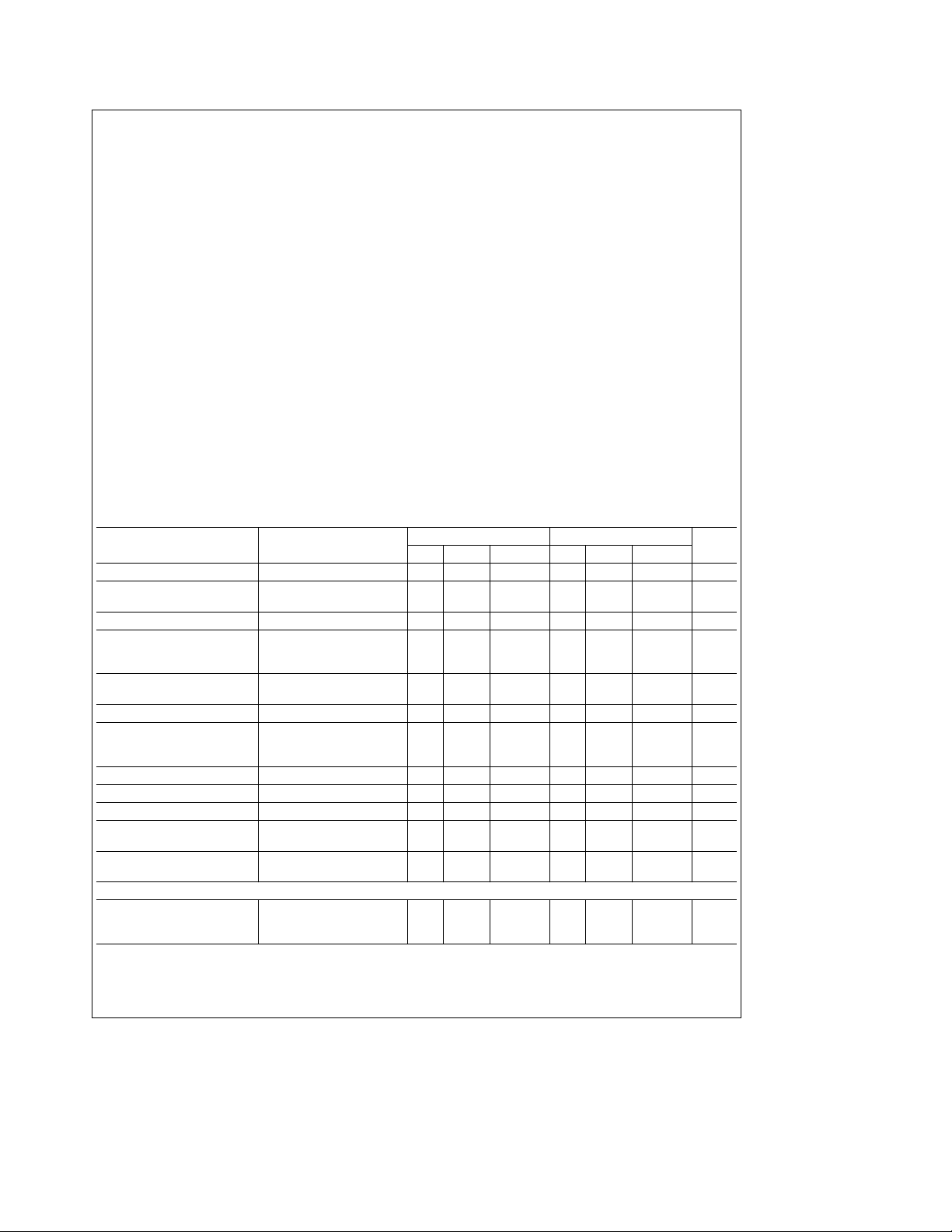
Electrical Characteristics (V
e
5VDC; specifications apply to both amplifiers unless otherwise stated)
(Note 4)
Parameter Conditions
Input Offset Voltage T
Input Bias Current IN(a)orIN(b), T
Input Offset Current IN(a)bIN(b), T
Input Common-Mode Voltage V
Range (Note 7) (LM2924, 0 V
Supply Current R
Supply Current R
Amplifier-to-Amplifier Coupling fe1 kHz to 20 kHz,
e
25§C, (Note 5)
A
(Note 6), V
V
(LM2924, V
T
(Note 8)
CM
a
e
30 VDC,T
a
e
26 VDC)
a
e %
,V
L
L
A
a
a
e %
,V
e
25§C, Input Referred,
e
A
e
0V
e
A
e
A
e
30V,
e
26V)
e
5V 0.5 1 0.5 1 mA
Min Typ Max Min Typ Max
25§C,
25§C
25§C,
Input Offset Voltage (Note 5)
Input Bias Current IN(a)orIN(b) 400 500 nA
Input Offset Current IN(a)bIN(b) 150 200 nA
a
Input Common-Mode Voltage V
Range (LM2924, V
Differential Input Voltage Keep All VIN’st0V
e
30 VDC, (Note 7)
a
e
26 VDC)
(or Vb, if Used), (Note 9)
DC
OP AMP ONLY
a
Large Signal Voltage Gain V
e
15 VDC,Voswing
1VDCto 11 VDC, 25 100 25 100 V/mV
e
R
2kX,T
L
A
e
e
25§C
LM392 LM2924
32V org16V 26V org13V
b
0.3V toa32V
Ctoa70§C
§
b
65§Ctoa150§C
C 260§C
§
C 215§C
§
C 220§C
§
b
0.3V toa26V
b
40§Ctoa85§C
b
65§Ctoa150§C
LM392 LM2924
g
g
2
5
g
g
2
7mV
50 250 50 250 nA
g
g
5
50
a
b
1.5 0 V
g
g
5
50 nA
a
b
1.5 V
12 1 2mA
b
100
g
7
a
b
0V
20 V
b
100 dB
g
10 mV
a
b
2V
32 26 V
Units
2

a
Electrical Characteristics (V
e
5VDC; specifications apply to both amplifiers unless otherwise stated)
(Note 4) (Continued)
Parameter Conditions
LM392 LM2924
Min Typ Max Min Typ Max
Units
OP AMP ONLY
Output Voltage Swing R
L
(LM2924, R
Common-Mode Rejection DC, T
Ratio 0 V
Power Supply Rejection Ratio DC, T
Output Current Source V
V
V
IN(a)
IN(b)
a
2VDC,T
Output Current Sink V
V
V
IN(b)
IN(a)
a
2VDC,T
V
IN(b)
V
IN(a)
a
V
200 mV, T
Input Offset Voltage Drift R
Input Offset Current Drift R
S
S
e
A
DC
A
e
e
e
e
e
e
2kX,T
e
to V
e
e
e
15 VDC,V
A
e
e
15 VDC,V
A
e
e
15 VDC,V
25§C,
A
t
L
25§C, V
a
b
1.5 V
10 kX)
CM
DC
0V
e
65 70 50 70 dB
a
b
1.5 0 V
a
b
1.5
25§C 65 100 50 100 dB
1VDC,
0VDC,
e
25§C
e
o
20 40 20 40 mA
1VDC,
0VDC,
e
25§C
e
o
10 20 10 20 mA
1VDC,
0VDC,
e
A
o
25§C
e
12 50 12 50 mA
0X 77mV/§C
0X 10 10 pADC/§C
COMPARATOR ONLY
Voltage Gain R
Large Signal Response Time V
Response Time V
Output Sink Current V
Saturation Voltage V
Output Leakage Current V
Note 1: For operating at temperatures above 25§C, the LM392 and the LM2924 must be derated based on a 125§C maximum junction temperature and a thermal
resistance of 122
use external resistors, where possible, to allow the amplifier to saturate or to reduce the power which is dissipated in the integrated circuit.
Note 2: Short circuits from the output to V
current is approximately 40 mA for the op amp and 30 mA for the comparator independent of the magnitude of V
continuous short circuits can exceed the power dissipation ratings and cause eventual destruction.
Note 3: This input current will only exist when the voltage at any of the input leads is driven negative. It is due to the collector-base junction of the input PNP
transistors becoming forward biased and thereby acting as input diode clamps. In addition to this diode action, there is also lateral NPN parasitic transistor action
on the IC chip. This transistor action can cause the output voltages of the amplifiers to go to the V
duration that an input is driven negative. This is not destructive and normal output states will re-establish when the input voltage, which was negative, again returns
to a value greater than
C/W which applies for the device soldered in a printed circuit board, operating in still air ambient. The dissipation is the total of both amplifiersÐ
§
b
0.3V (at 25§C).
t
L
e
T
A
e
IN
V
REF
e
V
RL
e
T
A
e
RL
e
T
A
IN(b)
V
IN(a)
t
V
o
IN(b)
V
IN(a)
I
SINK
V
IN(b)
V
IN(a)
I
SINK
IN(b)
V
IN(a)
e
V
o
V
IN(b)
V
IN(a)
e
V
o
a
can cause excessive heating and eventual destruction. When considering short circuits to ground, the maximum output
a
15 kX,V
25§C
TTL Logic Swing,
e
5VDC,R
25§C
5VDC,R
25§C, (Note 10)
e
e
1.5 VDC,T
t
e
s
t
e
s
e
t
5VDC,T
e
t
30 V
e
1.4 V
DC
e
L
e
L
15 VDC,
5.1 kX,
5.1 kX,
50 200 25 100 V/mV
300 300 ns
1.3 1.5 ms
1VDC,
0VDC, 6 16 6 16 mA
e
25§C
A
1VDC,
0, 250 400 400 mV
e
4 mA, T
25§C
A
1VDC,
0, 700 700 mV
4mA
0,
1VDC, 0.1 0.1 nA
e
25§C
A
0,
1VDC, 1.0 1.0 mA
DC
a
. At values of supply voltage in excess of 15V,
a
voltage level (or to ground for a large overdrive) for the time
V
3

a
Note 4: These specifications apply for V
the LM2924 temperature specifications are limited to
Note 5: At output switch point, V
Note 6: The direction of the input current is out of the IC due to the PNP input stage. This current is essentially constant, independent of the state of the output
so no loading change exists on the input lines.
Note 7: The input common-mode voltage or either input signal voltage should not be allowed to go negative by more than 0.3V. The upper end of the
common-mode voltage range is V
Note 8: Due to proximity of external components, insure that coupling is not originating via the stray capacitance between these external parts. This typically
can be detected as this type of capacitive increases at higher frequencies.
Note 9: Positive excursions of input voltage may exceed the power supply level. As long as the other input voltage remains within the common-mode range,
the comparator will provide a proper output state. The input voltage to the op amp should not exceed the power supply level. The input voltage state must not
be less than
Note 10: The response time specified is for a 100 mV input step with 5 mV overdrive. For larger overdrive signals 300 ns can be obtained.
b
0.3V (or 0.3V below the magnitude of the negative power supply, if used) on either amplifier.
e
5V, unless otherwise stated. For the LM392, temperature specifications are limited to 0§CsT
j
1.4V, R
O
a
b
1.5V, but either or both inputs can go to 32V without damage (26V for LM2924).
b
e
0X with Vafrom 5V to 30V; and over the full input common-mode range (0V to V
S
40§CsT
s
a
85§C.
A
s
a
70§C and
A
a
b
1.5V).
Schematic Diagram
Application Hints
Please refer to the application hints section of the LM193 and the LM158 datasheets.
4
TL/H/7793– 2

Physical Dimensions inches (millimeters)
Order Number LM392M or LM2924M
S.O. Package (M)
NS Package Number M08A
5

Physical Dimensions inches (millimeters) (Continued)
Molded Dual-In-Line Package (N)
Order Number LM392N or LM2924N
NS Package Number N08E
LIFE SUPPORT POLICY
LM392/LM2924 Low Power Operational Amplifier/Voltage Comparator
NATIONAL’S PRODUCTS ARE NOT AUTHORIZED FOR USE AS CRITICAL COMPONENTS IN LIFE SUPPORT
DEVICES OR SYSTEMS WITHOUT THE EXPRESS WRITTEN APPROVAL OF THE PRESIDENT OF NATIONAL
SEMICONDUCTOR CORPORATION. As used herein:
1. Life support devices or systems are devices or 2. A critical component is any component of a life
systems which, (a) are intended for surgical implant support device or system whose failure to perform can
into the body, or (b) support or sustain life, and whose be reasonably expected to cause the failure of the life
failure to perform, when properly used in accordance support device or system, or to affect its safety or
with instructions for use provided in the labeling, can effectiveness.
be reasonably expected to result in a significant injury
to the user.
National Semiconductor National Semiconductor National Semiconductor National Semiconductor
Corporation Europe Hong Kong Ltd. Japan Ltd.
1111 West Bardin Road Fax: (
Arlington, TX 76017 Email: cnjwge@tevm2.nsc.com Ocean Centre, 5 Canton Rd. Fax: 81-043-299-2408
Tel: 1(800) 272-9959 Deutsch Tel: (
Fax: 1(800) 737-7018 English Tel: (
National does not assume any responsibility for use of any circuitry described, no circuit patent licenses are implied and National reserves the right at any time without notice to change said circuitry and specifications.
Fran3ais Tel: (
Italiano Tel: (
a
49) 0-180-530 85 86 13th Floor, Straight Block, Tel: 81-043-299-2309
a
49) 0-180-530 85 85 Tsimshatsui, Kowloon
a
49) 0-180-532 78 32 Hong Kong
a
49) 0-180-532 93 58 Tel: (852) 2737-1600
a
49) 0-180-534 16 80 Fax: (852) 2736-9960
 Loading...