

LM391 Audio Power Driver
General Description
The LM391 audio power driver is designed to drive external
power transistors in 10 to 100 watt power amplifier designs.
High power supply voltage operation and true high fidelity
performance distinguish this IC. The LM391 is internally protected for output faults and thermal overloads; circuitry providing output transistor protection is user programmable.
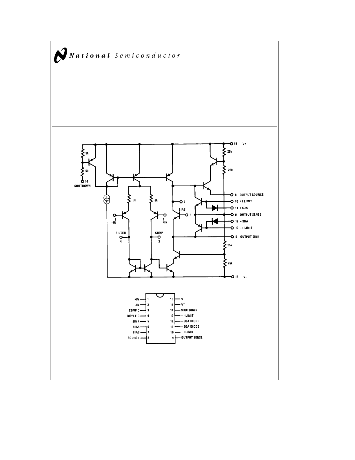
Equivalent Schematic and Connection Diagram
Features
Y
High Supply Voltage
Y
Low Distortion 0.01%
Y
Low Input Noise 3 mV
Y
High Supply Rejection 90 dB
Y
Gain and Bandwidth Selectable
Y
Dual Slope SOA Protection
Y
Shutdown Pin
December 1994
g
50V max
LM391 Audio Power Driver
Dual-In-Line Package
TL/H/7146– 1
Top View
TL/H/7146– 2
Order Number LM391N-100
See NS Package Number N16A
C
1995 National Semiconductor Corporation RRD-B30M115/Printed in U. S. A.
TL/H/7146
Absolute Maximum Ratings
If Military/Aerospace specified devices are required,
please contact the National Semiconductor Sales
Office/Distributors for availability and specifications.
Supply Voltage
LM391N-100
g
50V ora100V
Input Voltage Supply Voltage less 5V
Shutdown Current (Pin 14) 1 mA
Electrical Characteristics T
e
25§C (The following are for V
A
Parameter Conditions Min Typ Max Units
Quiescent Current Current in Pin 15
LM391N-100 V
e
056
IN
Output Swing Positive V
Negative V
Drive Current Source (Pin 8) 5 mA
Sink (Pin 5) 5 mA
Noise (20 Hz–20 kHz) Input Referred 3 mV
Supply Rejection Input Referred 70 90 dB
Total Harmonic Distortion fe1 kHz 0.01 %
e
f
20 kHz 0.10 0.25 %
Intermodulation Distortion 60 Hz, 7 kHz, 4:1 0.01 %
Open Loop Gain fe1 kHz 1000 5500 V/V
Input Bias Current 0.1 1.0 mA
Input Offset Voltage 5 20 mV
Positive Current Limit V
Negative Current Limit V
BE
BE
Pin 10–9 650 mV
Pin 9–13 650 mV
Positive Current Limit Bias Current Pin 10 10 100 mA
Negative Current Limit Bias Current Pin 13 10 100 mA
Pin 14 Current Comments
Minimum pin 14 current required for shutdown is 0.5 mA, and must not exceed 1 mA.
Maximum pin 14 current for amplifier not shut down is 0.05 mA.
The typical shutdown switch point current is 0.2 mA.
Note 1: For operation in ambient temperatures above 25§C, the device must be derated based on a 150§C maximum junction temperature and a thermal resistance
C/W junction to ambient.
of 90
§
Package Dissipation (Note 1) 1.39W
Storage Temperature
b
65§Ctoa150§C
Operating Temperature 0§Ctoa70§C
Lead Temp. (Soldering, 10 sec.) 260§C
Thermal Resistance
i
JC
i
JA
a
e
90% V
a
MAX
and V
b
e
90% V
b
20§C/W
63§C/W
MAX
.)
mA
a
b
7V
b
a
7V
a
b
5V
b
a
5V
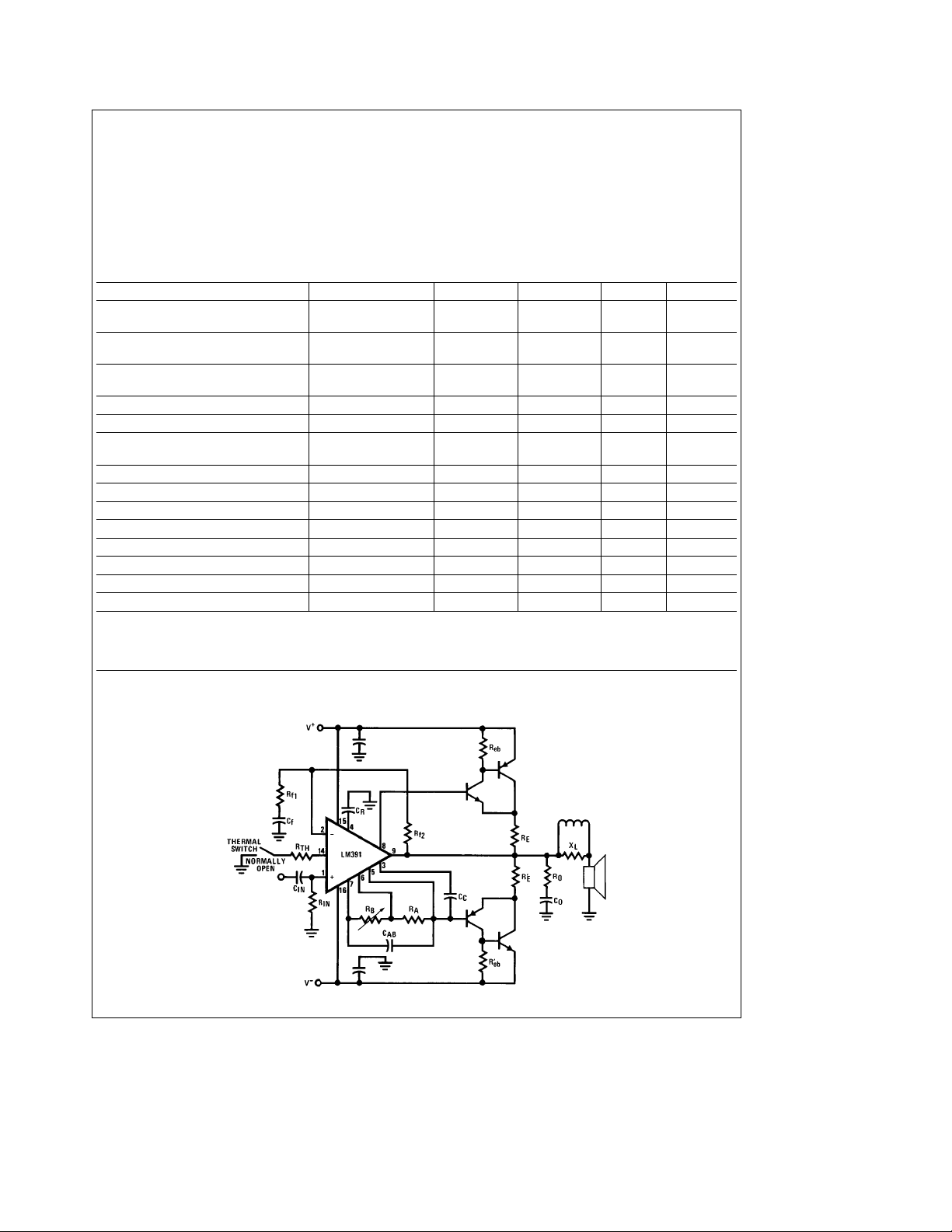
Typical Applications
FIGURE 1. LM391 with External ComponentsÐProtection Circuitry Not Shown
TL/H/7146– 3
2
Typical Performance Characteristics
Output Power vs Supply Voltage Frequency (R
Total Harmonic Distortion vs
e
8X)
L
Input Referred Power Supply
Open Loop Gain vs Frequency Rejection vs Frequency
Total Harmonic Distortion vs
Frequency (R
e
4X)
L
Total Harmonic Distortion vs
AB Bias Current
TL/H/7146– 4
Pin Descriptions
Pin No. Pin Name Comments
1
2
3 Compensation Sets the dominant pole
4 Ripple Filter Improves negative supply rejection
5 Sink Output Drives output devices and is emitter of AB bias V
6 BIAS Base of V
7 BIAS Collector of V
8 Source Output Drives output devices
9 Output Sense Biases the IC and is used in protection circuits
10
11
12
13
14 Shutdown Shuts off amplifier when current is pulled out of pin
15 V
16 V
a
Input Audio input
b
Input Feedback input
multiplier
BE
multiplier
BE
a
Current Limit Base of positive side protection circuit transistor
a
SOA Diode Diode used for dual slope SOA protection
b
SOA Diode Diode used for dual slope SOA protection
b
Current Limit Base of negative side protection circuit transistor
a
b
Positive supply
Negative supply
3
multiplier
BE
External Components (Figure 1)
Component Typical Value Comments
C
IN
R
IN
R
f
2
R
f
1
C
f
C
C
R
A
R
B
C
AB
C
R
R
eb
R
O
C
O
R
E
R
TH
C2,C
X
L
Ê
2
1 mF Input coupling capacitor sets a low frequency pole with RIN.
1
e
f
L
2qRINC
IN
100k Sets input impedance and DC bias to input.
100k Feedback resistor; for minimum offset voltage at the output this should be equal to RIN.
5.1k Feedback resistor that works with R
R
f
A
e1a
V
2
R
f
1
to set the voltage gain.
f
2
10 mF Feedback capacitor. This reduces the gain to unity at DC for minimum offset voltage at the
output. Also sets a low frequency pole with R
1
e
f
L
2qR
C
f
f
1
.
f
1
5 pF Compensation capacitor. Sets gain bandwidth product and a high frequency pole.
1
e
GBW
2q5000C
Max fhfor stable design&500 kHz.
GBW
e
,f
h
A
C
V
3.9k AB bias resistor.
10k AB bias potentiometer. Adjust to set bias current in the output stage.
0.1 mF Bypass capacitor for bias. This improves high frequency distortion and transient response.
5 pF Ripple capacitor. This improves negative supply rejection at midband and high frequencies.
C
, if used, must equal CC.
R
100X Bleed resistor. This removes stored charge in output transistors.
2.7X Output compensation resistor. This resistor and COcompensate the output stage. This value
will vary slightly for different output devices.
0.1 mF Output compensation capacitor. This works with ROto form a zero that cancels fbof the
output power transistors.
0.3X Emitter degeneration resistor. This resistor gives thermal stability to the output stage
quiescent current. IRC PW5 type.
39k Shutdown resistor. Sets the amount of current pulled out of pin 14 during shutdown.
1000 pF Compensation capacitors for protection circuitry.
10Xll5 m H Used to isolate capacitive loads, usually 20 turns of wire wrapped around a 10X, 2W resistor.
4
 Loading...