


LM3915
Dot/Bar Display Driver
General Description
The LM3915 is a monolithic integrated circuit that senses
analog voltage levels and drives ten LEDs, LCDs or vacuum
fluorescent displays, providing a logarithmic 3 dB/step analog display.Onepinchanges the display from a bar graph to
a moving dot display. LED current driveisregulated and programmable, eliminating the need for current limiting resistors. The whole display system can operate from a single
supply as low as 3V or as high as 25V.
The IC contains an adjustable voltage reference and an accurate ten-step voltage divider. The high-impedance input
buffer accepts signals down to ground and up to within 1.5V
of the positive supply.Further, it needs no protection against
inputs of
±
35V. The input buffer drives 10 individual comparators referenced to the precision divider.Accuracy is typically better than 1 dB.
The LM3915’s 3 dB/step display is suited for signals with
wide dynamic range, such as audio level, power, light intensity or vibration. Audio applications include average or peak
level indicators, power meters and RF signal strength
meters. Replacing conventional meters with an LED bar
graph results in a faster responding, more rugged display
with high visibility that retains the ease of interpretation of an
analog display.
The LM3915 is extremely easy to apply. A 1.2V full-scale
meter requires only one resistor in addition to the ten LEDs.
One more resistor programs the full-scale anywhere from
1.2V to 12V independent of supply voltage. LED brightness
is easily controlled with a single pot.
The LM3915 is very versatile. The outputs can drive LCDs,
vacuum fluorescents and incandescent bulbs as well as
LEDs of any color. Multiple devices can be cascaded for a
dot or bar mode display with a range of 60 or 90 dB.
LM3915s can also be cascaded with LM3914s for a linear/
log display or with LM3916s for an extended-range VU
meter.
Features
n 3 dB/step, 30 dB range
n Drives LEDs, LCDs, or vacuum fluorescents
n Bar or dot display mode externally selectable by user
n Expandable to displays of 90 dB
n Internal voltage reference from 1.2V to 12V
n Operates with single supply of 3V to 25V
n Inputs operate down to ground
n Output current programmable from 1 mA to 30 mA
n Input withstands
±
35V without damage or false outputs
n Outputs are current regulated, open collectors
n Directly drives TTL or CMOS
n The internal 10-step divider is floating and can be
referenced to a wide range of voltages
The LM3915 is rated for operation from 0˚C to +70˚C. The
LM3915N-1 is available in an 18-lead molded DIP package.
January 2000
LM3915 Dot/Bar Display Driver
© 2000 National Semiconductor Corporation DS005104 www.national.com
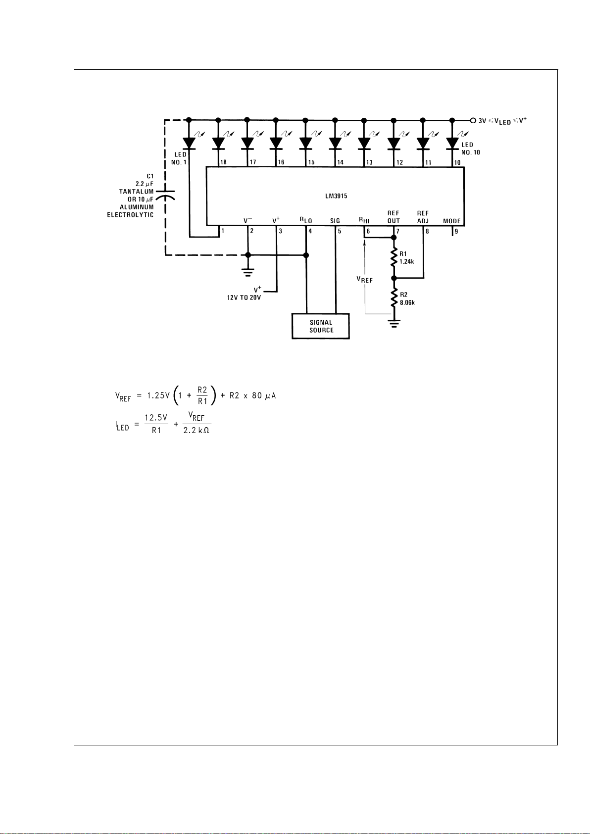
Typical Applications
0V to 10V Log Display
DS005104-1
Notes: Capacitor C1 is required if leads to the LED supply are 6" or longer.
Circuit as shown is wired for dot mode. For bar mode, connect pin 9 to pin 3. V
LED
must be kept below 7V or dropping resistor should be used to limit IC power
dissipation.
LM3915
www.national.com 2
Absolute Maximum Ratings (Note 1)
If Military/Aerospace specified devices are required,
please contact the National Semiconductor Sales Office/
Distributors for availability and specifications.
Power Dissipation (Note 6)
Molded DIP(N) 1365 mW
Supply Voltage 25V
Voltage on Output Drivers 25V
Input Signal Overvoltage (Note 4)
±
35V
Divider Voltage −100 mV to V
+
Reference Load Current 10 mA
Storage Temperature Range −55˚C to +150˚C
Lead Temperature
(Soldering, 10 sec.) 260˚C
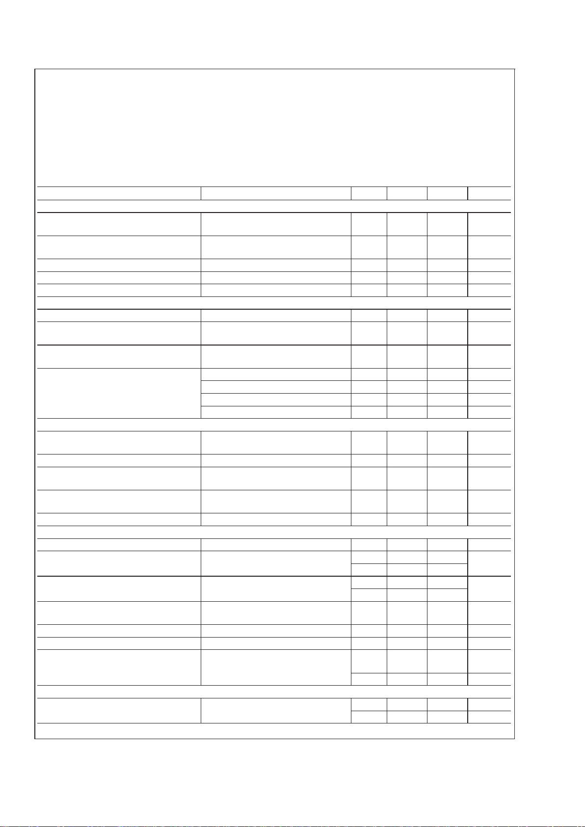
Electrical Characteristics (Notes 2, 4)
Parameter Conditions (Note 2) Min Typ Max Units
COMPARATOR
Offset Voltage, Buffer and First
Comparator
0V ≤ V
RLO
=
V
RHI
≤ 12V,
I
LED
=
1mA
310mV
Offset Voltage, Buffer and Any Other
Comparator
0V ≤ V
RLO
=
V
RHI
≤ 12V,
I
LED
=
1mA
315mV
Gain (∆I
LED
/∆VIN)I
L(REF)
=
2 mA, I
LED
=
10 mA 3 8 mA/mV
Input Bias Current (at Pin 5) 0V ≤ V
IN
≤ (V+− 1.5V) 25 100 nA
Input Signal Overvoltage No Change in Display −35 35 V
VOLTAGE-DIVIDER
Divider Resistance Total, Pin 6 to 4 16 28 36 kΩ
Relative Accuracy (Input Change
Between Any Two Threshold Points)
(Note 3)
2.0 3.0 4.0 dB
Absolute Accuracy at Each Threshold
Point
(Note 3)
V
IN
= −3, −6 dB −0.5 +0.5 dB
V
IN
= −9 dB −0.5 +0.65 dB
V
IN
= −12, −15, −18 dB −0.5 +1.0 dB
V
IH
= −21, −24, −27 dB −0.5 +1.5 dB
VOLTAGE REFERENCE
Output Voltage 0.1 mA ≤ I
L(REF)
≤ 4 mA,
V
+
=
V
LED
=
5V
1.2 1.28 1.34 V
Line Regulation 3V ≤ V
+
≤ 18V 0.01 0.03
%
/V
Load Regulation 0.1 mA ≤ I
L(REF)
≤ 4 mA,
V
+
=
V
LED
=
5V
0.4 2
%
Output Voltage Change with
Temperature
0˚C ≤ T
A
≤ +70˚C, I
L(REF)
=
1 mA,
V
+
=
V
LED
5V
1
%
Adjust Pin Current 75 120 µA
OUTPUT DRIVERS
LED Current V
+
=
V
LED
=
5V, I
L(REF)
=
1 mA 7 10 13 mA
LED Current Difference (Between
Largest and Smallest LED Currents)
V
LED
= 5V, I
LED
=
2mA
V
LED
= 5V, I
LED
20 mA
0.12 0.4
mA
1.2 3
LED Current Regulation 2V ≤ V
LED
≤ 17V, I
LED
=2mA
I
LED
=20mA
0.1 0.25
mA
13
Dropout Voltage I
LED(ON)
=
20 mA,
@
V
LED
=
5V,
∆I
LED
=
2mA
1.5 V
Saturation Voltage I
LED
=
2.0 mA, I
L(REF)
=
0.4 mA 0.15 0.4 V
Output Leakage, Each Collector (Bar Mode) (Note 5) 0.1 10 µA
Output Leakage
Pins 10–18
(Dot Mode) (Note 5)
0.1 10 µA
Pin 1 60 150 450 µA
SUPPLY CURRENT
Standby Supply Current
(All Outputs Off)
V
+
=
+5V, I
L(REF)
=
0.2 mA
V
+
=
+20V, I
L(REF)
=
1.0 mA
2.4 4.2 mA
6.1 9.2 mA
LM3915
www.national.com3
Electrical Characteristics (Notes 2, 4) (Continued)
Note 1: AbsoluteMaximumRatingsindicate limits beyond which damage to the device may occur.OperatingRatingsindicate conditions for which the device is func-
tional, but do not guarantee specific performance limits. Electrical Characteristics state DC and AC electrical specifications under particular test conditions which guarantee specific performance limits. This assumes that the device is within the Operating Ratings. Specifications are not guaranteed for parameters where no limit is
given, however, the typical value is a good indication of device performance.
Note 2: Unless otherwise stated, all specifications apply with the following conditions:
3V
DC
≤ V+≤ 20 V
DC
−0.015V ≤ V
RLO
≤ 12 V
DC
T
A
=
25˚C, I
L(REF)
=
0.2 mA, pin 9 connected to pin 3 (bar mode).
3V
DC
≤ V
LED
≤ V
+
V
REF,VRHI,VRLO
≤ (V+− 1.5V) For higher power dissipations, pulse testing is used.
−0.015V ≤ V
RHI
≤ 12 V
DC
0V ≤ VIN≤ V+− 1.5V
Note 3: Accuracy is measured referred to 0 dB=+ 10.000 V
DC
at pin 5, with + 10.000 VDCat pin 6, and 0.000 VDCat pin 4. At lower full scale voltages, buffer and
comparator offset voltage may add significant error. See table for threshold voltages.
Note 4: Pin 5 input current must be limited to
±
3 mA. The addition of a 39k resistor in series with pin 5 allows±100V signals without damage.
Note 5: Bar mode results when pin 9 is within 20 mV of V
+
. Dot mode results when pin 9 is pulled at least 200 mV below V+. LED#10 (pin 10 output current) is dis-
abled if pin 9 is pulled 0.9V or more below V
LED
.
Note 6: The maximum junction temperature of the LM3915 is 100˚C. Devices must be derated for operation at elevated temperatures. Junction to ambient thermal
resistance is 55˚C/W for the molded DIP (N package).
Threshold Voltage (Note 3)
Output dB Min Typ Max Output dB Min Typ Max
1 −27 0.422 0.447 0.531 6 −12 2.372 2.512 2.819
2 −24 0.596 0.631 0.750 7 −9 3.350 3.548 3.825
3 −21 0.841 0.891 1.059 8 −6 4.732 5.012 5.309
4 −18 1.189 1.259 1.413 9 −3 6.683 7.079 7.498
5 −15 1.679 1.778 1.995 10 0 9.985 10 10.015
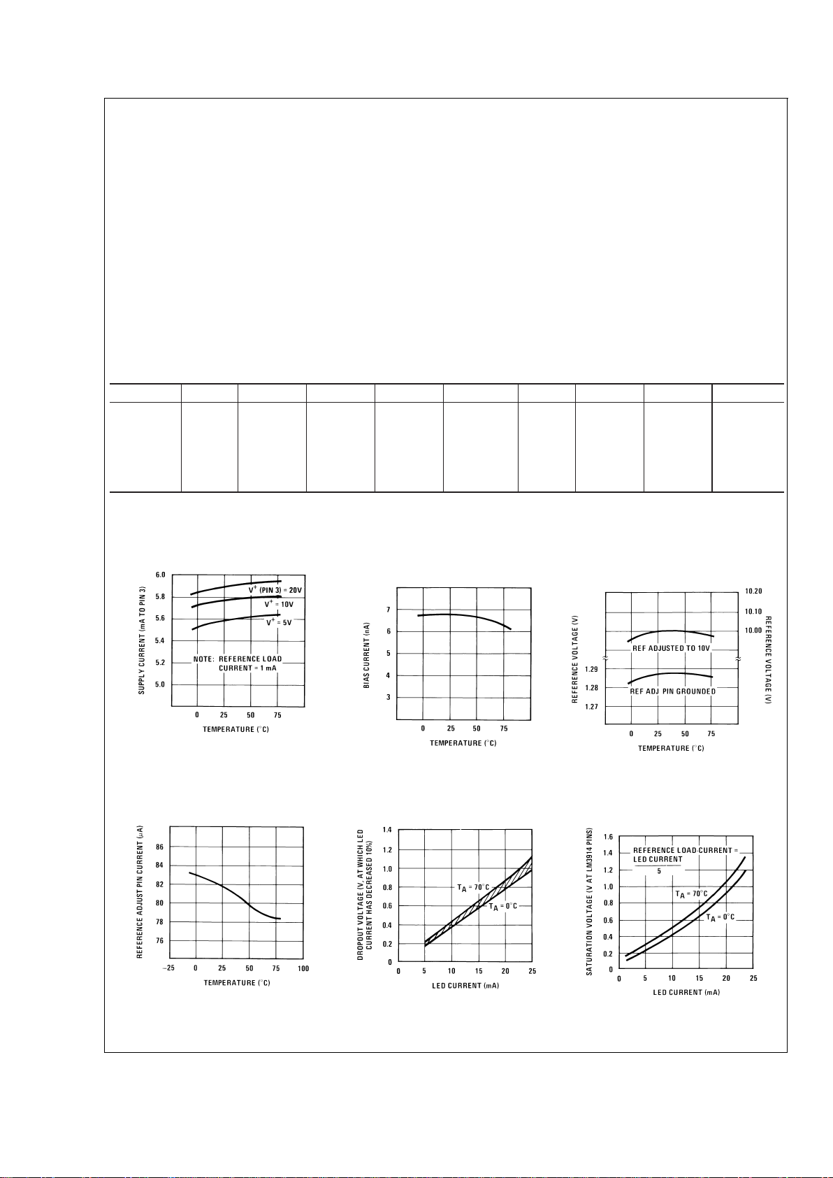
Typical Performance Characteristics
Supply Current vs Temperature
DS005104-34
Operating Input Bias Current vs
Temperature
DS005104-35
Reference Voltage vs
Temperature
DS005104-36
Reference Adjust Pin
Current vs Temperature
DS005104-37
LED Current-Regulation
Dropout
DS005104-38
LED Driver Saturation
Voltage
DS005104-39
LM3915
www.national.com 4
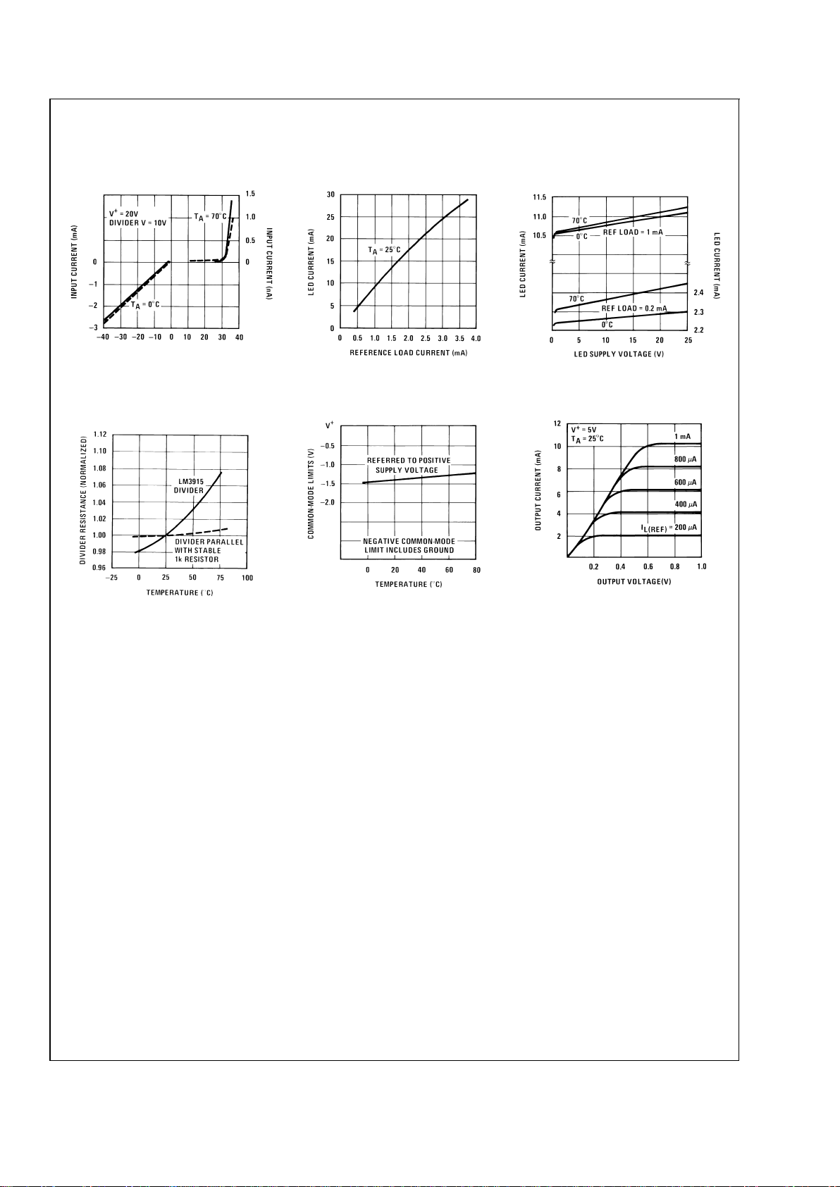
Typical Performance Characteristics (Continued)
Input Current Beyond
Signal Range (Pin 5)
DS005104-40
LED Current vs
Reference Loading
DS005104-41
LED Driver Current
Regulation
DS005104-42
Total Divider Resistance
vs Temperature
DS005104-43
Common-Mode Limits
DS005104-44
Output Characteristics
DS005104-45
LM3915
www.national.com5
Block Diagram (Showing Simplest Application)
DS005104-4
LM3915
www.national.com 6
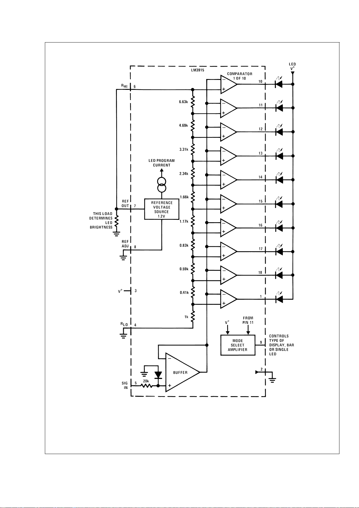
Functional Description
The simplified LM3915 block diagram is included to give the
general idea of the circuit’s operation. A high input impedance buffer operates with signals from ground to 12V, and is
protected against reverse and overvoltage signals. The signal is then applied to a series of 10 comparators; each of
which is biased to a different comparison level by the resistor
string.
In the example illustrated, the resistor string is connected to
the internal 1.25V reference voltage. In this case, for each
3 dB that the input signal increases, a comparator will switch
on another indicating LED. This resistor divider can be connected between any 2 voltages, providing that they are at
least 1.5V below V
+
and no lower than V−.
INTERNAL VOLTAGE REFERENCE
The reference is designed to be adjustable and develops a
nominal 1.25V between the REF OUT (pin 7) and REF ADJ
(pin 8) terminals. The reference voltage is impressed across
program resistor R1 and, since the voltage is constant, a
constant current I
1
then flows through the output set resistor
R2 giving an output voltage of:
Since the 120 µA current (max) from the adjust terminal represents an error term, the reference was designed to minimize changes of this current with V
+
and load changes. For
correct operation, reference load current should be between
80 µA and 5 mA. Load capacitance should be less than
0.05 µF.
CURRENT PROGRAMMING
A feature not completely illustrated by the block diagram is
the LED brightness control. The current drawn out of the reference voltage pin (pin 7) determines LED current. Approximately 10 times this current will be drawn through each
lighted LED, and this current will be relatively constant despite supply voltage and temperature changes. Current
drawn by the internal 10-resistor divider,as well as by the external current and voltage-setting divider should be included
in calculating LED drive current. The ability to modulate LED
brightness with time, or in proportion to input voltage and
other signals can lead to a number of novel displays or ways
of indicating input overvoltages, alarms, etc.
The LM3915 outputs are current-limited NPN transistors as
shown below. An internal feedback loop regulates the transistor drive. Output current is held at about 10 times the reference load current, independent of output voltage and processing variables, as long as the transistor is not saturated.
Outputs may be run in saturation with no adverse effects,
making it possible to directly drive logic. The effective saturation resistance of the output transistors, equal to R
E
plus the
transistors’ collector resistance, is about 50Ω. It’s also possible to drive LEDs from rectified AC with no filtering. To
avoid oscillations, the LED supply should be bypassed with a
2.2 µF tantalum or 10 µF aluminum electrolytic capacitor.
MODE PIN USE
Pin 9, the Mode Select input, permits chaining of multiple
LM3915s, and controls bar or dot mode operation. The following tabulation shows the basic ways of using this input.
Other more complex uses will be illustrated in the applications.
Bar Graph Display: Wire Mode Select (pin 9)
directly
to pin
3(V
+
pin).
Dot Display, Single LM3915 Driver: Leave the Mode Select
pin open circuit.
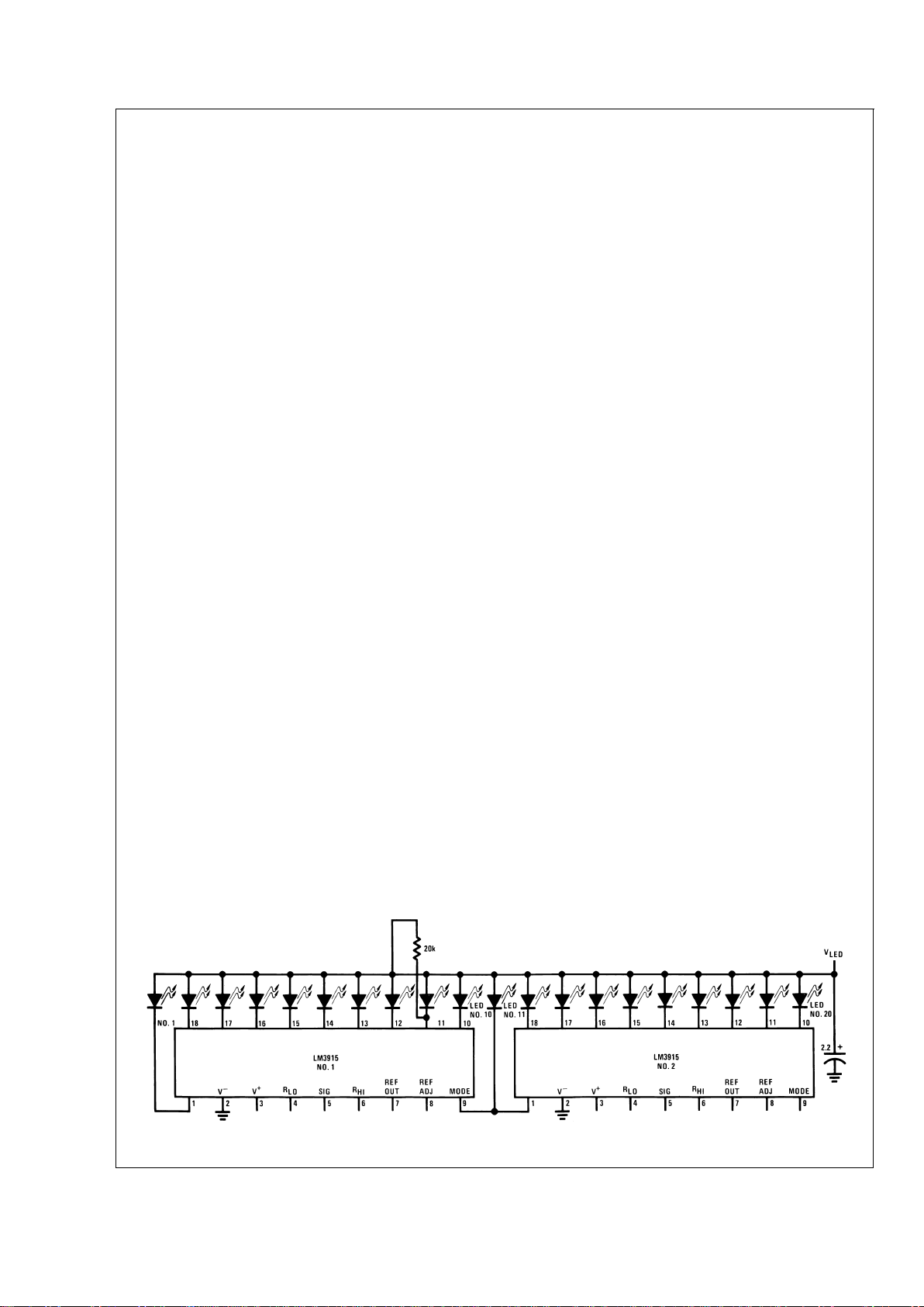
Dot Display, 20 or More LEDs: Connect pin 9 of the
first
driver in the series (i.e., the one with the lowest input voltage
comparison points) to pin 1 of the next higher LM3915 driver.
Continue connecting pin 9 of lower input drivers to pin 1 of
higher input drivers for 30 or more LED displays. The last
LM3915 driver in the chain will have pin 9 left open. All previous drivers should have a 20k resistor in parallel with LED
#
9 (pin 11 to V
LED
).
Mode Pin Functional Description
This pin actually performs two functions. Refer to the simplified block diagram below.
DS005104-5
LM3915 Output Circuit
DS005104-6
Block Diagram of Mode Pin Function
DS005104-7
*
High for bar
LM3915
www.national.com7
Mode Pin Functional Description
(Continued)
DOT OR BAR MODE SELECTION
The voltage at pin 9 is sensed by comparator C1, nominally
referenced to (V
+
− 100 mV). The chip is in bar mode when
pin 9 is above this level; otherwise it’s in dot mode. The comparator is designed so that pin 9 can be left open circuit for
dot mode.
Taking into account comparator gain and variation in the
100 mV reference level, pin 9 should be no more than 20 mV
below V
+
for bar mode and more than 200 mV below V+(or
open circuit) for dot mode. In most applications, pin 9 is either open (dot mode) or tied to V
+
(bar mode). In bar mode,
pin 9 should be connected directly to pin 3. Large currents
drawn from the power supply (LED current, for example)
should not share this path so that large IR drops are avoided.
DOT MODE CARRY
In order for the display to make sense when multiple
LM3915s are cascaded in dot mode, special circuitry has
been included to shut off LED
#
10 of the first device when
LED
#
1 of the second device comes on. The connection for
cascading in dot mode has already been described and is
depicted below.
As long as the input signal voltage is below the threshold of
the second LM3915, LED
#
11is off. Pin 9 of LM3915#1 thus
sees effectively an open circuit so the chip is in dot mode. As
soon as the input voltage reaches the threshold of LED
#
11,
pin 9 of LM3915
#
1 is pulled an LED drop (1.5V or more) be-
low V
LED
. This condition is sensed by comparator C2, refer-
enced 600 mV below V
LED
. This forces the output of C2 low,
which shuts off output transistor Q2, extinguishing LED
#
10.
V
LED
is sensed via the 20k resistor connected to pin 11. The
very small current (less than 100 µA) that is diverted from
LED
#
9 does not noticeably affect its intensity.
An auxiliary current source at pin 1 keeps at least 100 µA
flowing through LED
#
11 even if the input voltage rises high
enough to extinguish the LED. This ensures that pin 9 of
LM3915
#
1 is held low enough to force LED#10 off when
any
higher LED is illuminated. While 100 µA does not normally produce significant LED illumination, it may be noticeable when using high-efficiency LEDs in a dark environment.
If this is bothersome, the simple cure is to shunt LED
#
11
with a 10k resistor. The 1V IR drop is more than the 900 mV
worst case required to hold off LED
#
10 yet small enough
that LED
#
11 does not conduct significantly.
OTHER DEVICE CHARACTERISTICS
The LM3916 is relatively low-powered itself, and since any
number of LEDs can be powered from about 3V, it is a very
efficient display driver. Typical standby supply current (all
LEDs OFF) is 1.6 mA. However, any reference loading adds
4 times that current drain to the V
+
(pin 3) supply input. For
example, an LM3916 witha1mAreference pin load (1.3k)
would supply almost 10 mA to every LED while drawing only
10 mA from its V
+
pin supply. At full-scale, the IC is typically
drawing less than 10%of the current supplied to the display.
The display driver does not have built-in hysteresis so that
the display does not jump instantly from one LED to the next.
Under rapidly changing signal conditions, this cuts down
high frequency noise and often an annoying flicker.An “overlap” is built in so that at no time are all segments completely
off in the dot mode. Generally 1 LED fades in while the other
fades out over a mV or more of range. The change may be
much more rapid between LED
#
10 of one device and LED
#
1ofa
second
device “chained” to the first.
Application Hints
The most difficult problem occurs when large LED currents
are being drawn, especially in bar graph mode. These currents flowing out of the ground pin cause voltage drops in external wiring, and thus errors and oscillations. Bringing the
return wires from signal sources, reference ground and bottom of the resistor string to a single point very near pin 2 is
the best solution.
Long wires from V
LED
to LED anode common can cause oscillations. Depending on the severity of the problem 0.05 µF
to 2.2 µF decoupling capacitors from LED anode common to
pin 2 will damp the circuit. If LED anode line wiring is inaccessible, often similar decoupling from pin 1 to pin 2 will be
sufficient.
If LED turn ON seems slow (bar mode) or several LEDs light
(dot mode), oscillation or excessive noise is usually the problem. In cases where proper wiring and bypassing fail to stop
oscillations, V
+
voltage at pin 3 is usually below suggested
limits. Expanded scale meter applications may have one or
both ends of the internal voltage divider terminated at relatively high value resistors. These high-impedance ends
should be bypassed to pin 2 with at least a 0.001 µF capacitor, or up to 0.1 µF in noisy environments.
Cascading LM3915s in Dot Mode
DS005104-8
LM3915
www.national.com 8
 Loading...