

LM3914
Dot/Bar Display Driver
General Description
The LM3914 is a monolithic integrated circuit that senses
analog voltage levels and drives 10 LEDs, providing a linear
analog display. Asingle pin changes the display from a moving dot toa bar graph. Current drive tothe LEDs is regulated
and programmable, eliminating the need for resistors. This
feature isone that allows operationof the wholesystem from
less than 3V.
The circuit contains its own adjustable reference and accurate 10-step voltage divider. The low-bias-current input
buffer accepts signals down to ground, or V
−
, yet needs no
protection against inputs of 35V above or below ground.The
buffer drives 10 individual comparators referenced to the
precision divider. Indication non-linearity can thus be held
typically to
1
⁄
2
%
, even over a wide temperature range.
Versatility was designed into the LM3914 so that controller,
visual alarm, andexpanded scale functions are easily added
on to thedisplay system. The circuit candrive LEDs of many
colors, or low-current incandescent lamps. Many LM3914s
can be “chained” to form displays of 20 to over 100 segments. Both ends of the voltage divider are externally available so that 2 drivers can be made into a zero-center meter.
The LM3914is very easy to apply as ananalog meter circuit.
A 1.2V full-scale meter requires only 1 resistor and a single
3V to 15V supply in addition to the 10 display LEDs. If the 1
resistor is a pot, it becomes the LED brightness control. The
simplified block diagram illustrates this extremely simple external circuitry.
When in the dot mode, there is a small amount of overlap or
“fade” (about 1 mV) between segments.This assures that at
no time will all LEDs be “OFF”, and thus any ambiguous display is avoided. Various novel displays are possible.
Much of the display flexibility derives from the fact that all
outputs areindividual, DC regulatedcurrents. Variouseffects
can be achieved by modulating these currents. The individual outputs can drive a transistor as well as a LED at the
same time, so controller functions including “staging” control
can be performed. The LM3914 can also act as a programmer, or sequencer.
The LM3914 is rated for operation from 0˚C to +70˚C. The
LM3914N-1 is available in an 18-lead molded (N) package.
The following typical application illustrates adjusting of the
reference to a desiredvalue, and proper grounding for accurate operation, and avoiding oscillations.
Features
n Drives LEDs, LCDs or vacuum fluorescents
n Bar or dot display mode externally selectable by user
n Expandable to displays of 100 steps
n Internal voltage reference from 1.2V to 12V
n Operates with single supply of less than 3V
n Inputs operate down to ground
n Output current programmable from 2 mA to 30 mA
n No multiplex switching or interaction between outputs
n Input withstands
±
35V without damage or false outputs
n LED driver outputs are current regulated,
open-collectors
n Outputs can interface with TTL or CMOS logic
n The internal 10-step divider is floating and can be
referenced to a wide range of voltages
January 2000
LM3914 Dot/Bar Display Driver
© 2000 National Semiconductor Corporation DS007970 www.national.com
Typical Applications
0V to 5V Bar Graph Meter
DS007970-1
Note: Grounding method is typical of
all
uses. The 2.2 µF tantalum or 10 µF aluminum electrolytic capacitor is needed if leads to the LED supply are 6" or
longer.
LM3914
www.national.com 2
Absolute Maximum Ratings (Note 1)
If Military/Aerospace specified devices are required,
please contact the National Semiconductor Sales Office/
Distributors for availability and specifications.
Power Dissipation (Note 6)
Molded DIP (N) 1365 mW
Supply Voltage 25V
Voltage on Output Drivers 25V
Input Signal Overvoltage (Note 4)
±
35V
Divider Voltage −100 mV to V
+
Reference Load Current 10 mA
Storage Temperature Range −55˚C to +150˚C
Soldering Information
Dual-In-Line Package
Soldering (10 seconds) 260˚C
Plastic Chip Carrier Package
Vapor Phase (60 seconds) 215˚C
Infrared (15 seconds) 220˚C
See AN-450 “Surface Mounting Methods and Their Effect
on Product Reliability” for other methods of soldering
surface mount devices.
Electrical Characteristics (Notes 2, 4)
Parameter Conditions (Note 2) Min Typ Max Units
COMPARATOR
Offset Voltage, Buffer and First
Comparator
0V ≤ V
RLO
=
V
RHI
≤ 12V,
I
LED
=
1mA
310mV
Offset Voltage, Buffer and Any Other
Comparator
0V ≤ V
RLO
=
V
RHI
≤ 12V,
I
LED
=
1mA
315mV
Gain (∆I
LED
/∆VIN)I
L(REF)
=
2 mA, I
LED
=
10 mA 3 8 mA/mV
Input Bias Current (at Pin 5) 0V ≤ V
IN
≤ V+− 1.5V 25 100 nA
Input Signal Overvoltage No Change in Display −35 35 V
VOLTAGE-DIVIDER
Divider Resistance Total, Pin 6 to 4 8 12 17 kΩ
Accuracy (Note 3) 0.5 2
%
VOLTAGE REFERENCE
Output Voltage 0.1 mA ≤ I
L(REF)
≤ 4 mA,
V
+
=
V
LED
=
5V
1.2 1.28 1.34 V
Line Regulation 3V ≤ V
+
≤ 18V 0.01 0.03
%
/V
Load Regulation 0.1 mA ≤ I
L(REF)
≤ 4 mA,
V
+
=
V
LED
=
5V
0.4 2
%
Output Voltage Change with
Temperature
0˚C ≤ T
A
≤ +70˚C, I
L(REF)
=
1 mA,
V
+
=
5V
1
%
Adjust Pin Current 75 120 µA
OUTPUT DRIVERS
LED Current V
+
=
V
LED
=
5V, I
L(REF)
=
1 mA 7 10 13 mA
LED Current Difference (Between
Largest and Smallest LED Currents)
V
LED
=
5V I
LED
=
2 mA 0.12 0.4
mA
I
LED
=
20 mA 1.2 3
LED Current Regulation 2V ≤ V
LED
≤ 17V I
LED
=
2 mA 0.1 0.25
mA
I
LED
=
20 mA 1 3
Dropout Voltage I
LED(ON)
=
20 mA, V
LED
=
5V,
∆I
LED
=
2mA
1.5 V
Saturation Voltage I
LED
=
2.0 mA, I
L(REF)
=
0.4 mA 0.15 0.4 V
Output Leakage, Each Collector (Bar Mode) (Note 5) 0.1 10 µA
Output Leakage (Dot Mode)
(Note 5)
Pins 10–18 0.1 10 µA
Pin 1 60 150 450 µA
SUPPLY CURRENT
Standby Supply Current
(All Outputs Off)
V
+
=
5V,
I
L(REF)
=
0.2 mA
2.4 4.2 mA
V
+
=
20V,
I
L(REF)
=
1.0 mA
6.1 9.2 mA
Note 1: Absolute Maximum Ratings indicate limits beyond whichdamage to thedevice may occur.OperatingRatings indicate conditionsfor which thedevice is functional, but do notguarantee specific performancelimits. Electrical CharacteristicsstateDC and AC electricalspecifications under particular testconditions which guarantee specific performance limits. This assumes that the device is within the Operating Ratings. Specifications are not guaranteed for parameters where no limit is
given, however, the typical value is a good indication of device performance.
LM3914
www.national.com3
Electrical Characteristics (Notes 2, 4) (Continued)
Note 2: Unless otherwise stated, all specifications apply with the following conditions:
3V
DC
≤ V+≤ 20 V
DCVREF,VRHI,VRLO
≤ (V+− 1.5V)
3V
DC
≤ V
LED
≤ V+0V ≤ VIN≤ V+− 1.5V
−0.015V ≤ V
RLO
≤ 12 V
DCTA
=
+25˚C, I
L(REF)
=
0.2 mA, V
LED
=
3.0V, pin 9 connected to pin 3 (Bar Mode).
−0.015V ≤ V
RHI
≤ 12 V
DC
For higher power dissipations, pulse testing is used.
Note 3: Accuracy is measured referred to +10.000 V
DC
at pin 6, with 0.000 VDCat pin 4. At lower full-scale voltages, buffer and comparator offset voltage may add
significant error.
Note 4: Pin 5 input current must be limited to
±
3 mA. The addition of a 39k resistor in series with pin 5 allows±100V signals without damage.
Note 5: Bar mode results when pin 9 is within 20 mV of V
+
. Dot mode results when pin 9 is pulled at least 200 mV below V+or left open circuit. LED No. 10 (pin
10 output current) is disabled if pin 9 is pulled 0.9V or more below V
LED
.
Note 6: The maximum junction temperature of the LM3914 is 100˚C. Devices must be derated for operation at elevated temperatures. Junction to ambient thermal
resistance is 55˚C/W for the molded DIP (N package).
Definition of Terms
Accuracy: The difference between the observed threshold
voltage and the ideal threshold voltage for each comparator.
Specified and tested with 10V across the internal voltage divider so that resistor ratio matching error predominates over
comparator offset voltage.
Adjust Pin Current: Current flowing outof the reference adjust pin when the reference amplifier is in the linear region.
Comparator Gain: The ratio of the change in output current
(I
LED
) to the change in input voltage (VIN) required to pro-
duce it for a comparator in the linear region.
Dropout Voltage: The voltage measured at the current
source outputs required to make the output current fall by
10%.
Input Bias Current: Current flowing out of the signal input
when the input buffer is in the linear region.
LED Current Regulation: The change in output current
over the specified range of LED supply voltage (V
LED
)as
measured at the current source outputs.As the forward voltage of an LED does not change significantly with a small
change in forward current, this is equivalent to changing the
voltage at the LED anodes by the same amount.
Line Regulation: The average change in reference output
voltage over the specified range of supply voltage (V
+
).
Load Regulation: The change in reference output voltage
(V
REF
) over the specified range of load current (I
L(REF)
).
Offset Voltage: The differential input voltage which must be
applied toeach comparator tobias the outputin the linearregion. Most significant error when the voltage across the internal voltage divider is small. Specified and tested with pin
6 voltage (V
RHI
) equal to pin 4 voltage (V
RLO
).
Typical Performance Characteristics
Supply Current vs
Temperature
DS007970-2
Operating Input Bias
Current vs Temperature
DS007970-20
Reference Voltage vs
Temperature
DS007970-21
LM3914
www.national.com 4
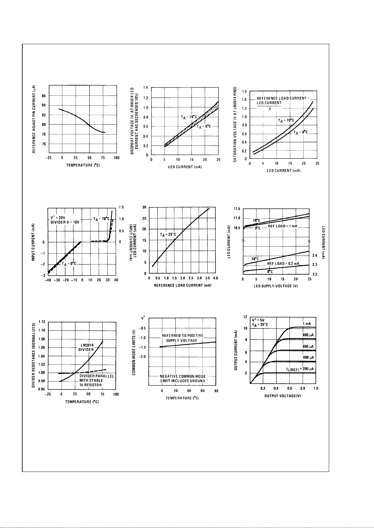
Typical Performance Characteristics (Continued)
Reference Adjust Pin
Current vs Temperature
DS007970-22
LED Current-Regulation
Dropout
DS007970-23
LED Driver Saturation
Voltage
DS007970-24
Input Current Beyond
Signal Range (Pin 5)
DS007970-25
LED Current vs
Reference Loading
DS007970-26
LED Driver Current
Regulation
DS007970-27
Total Divider Resistance
vs Temperature
DS007970-28
Common-Mode Limits
DS007970-29
Output Characteristics
DS007970-30
LM3914
www.national.com5
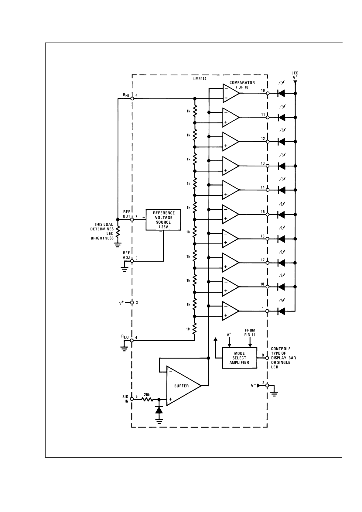
Block Diagram (Showing Simplest Application)
DS007970-3
LM3914
www.national.com 6

Functional Description
The simplifed LM3914 block diagram is to give the general
idea of the circuit’s operation. A high input impedance buffer
operates with signals from ground to 12V, and is protected
against reverse and overvoltage signals. The signal is then
applied to a series of 10 comparators; each of which is biased to a different comparison level by the resistor string.
In the example illustrated, the resistor string is connected to
the internal 1.25V reference voltage. In this case, for each
125 mV that the input signal increases, a comparator will
switch on another indicating LED. This resistor divider can
be connected between any 2 voltages, providing that they
are 1.5V below V
+
and no less than V−. If an expanded scale
meter display is desired, the total divider voltage can be as
little as 200 mV. Expanded-scale meter displays are more
accurate andthe segments light uniformlyonly if barmode is
used. At 50 mV or more per step, dot mode is usable.
INTERNAL VOLTAGE REFERENCE
The reference is designed to be adjustable and develops a
nominal 1.25V between the REF OUT (pin 7) and REF ADJ
(pin 8) terminals. The reference voltage is impressed across
program resistor R1 and, since the voltage is constant, a
constant current I
1
then flows through the output set resistor
R2 giving an output voltage of:
Since the 120 µAcurrent (max) from the adjust terminal represents an error term, the reference was designed to minimize changes of this current with V
+
and load changes.
CURRENT PROGRAMMING
A feature not completely illustrated by the block diagram is
the LED brightness control.The current drawn out of the reference voltage pin (pin 7) determines LED current. Approximately 10 times this current will be drawn through each
lighted LED, and this current will be relatively constant despite supply voltage and temperature changes. Current
drawn bythe internal 10-resistor divider,as well asby the external current and voltage-setting divider should be included
in calculating LED drive current. The ability to modulate LED
brightness with time, or in proportion to input voltage and
other signals can lead to a number of novel displaysor ways
of indicating input overvoltages, alarms, etc.
MODE PIN USE
Pin 9, the Mode Select input controls chaining of multiple
LM3914s, and controls bar or dot mode operation. The following tabulation shows the basic ways of using this input.
Other more complex uses will be illustrated in the applications.
Bar Graph Display: Wire Mode Select (pin 9)
directly
to pin
3(V
+
pin).
Dot Display, Single LM3914Driver: Leave theMode Select
pin open circuit.
Dot Display, 20 or More LEDs: Connect pin 9 of the
first
driver in theseries (i.e., the one with the lowest input voltage
comparison points)to pin 1 ofthe next higherLM3914 driver.
Continue connecting pin 9 of lower input drivers to pin 1 of
higher input drivers for 30, 40, or more LED displays. The
last LM3914driver in the chain willhave pin 9wired to pin11.
All previousdrivers should havea 20k resistor in parallel with
LED No. 9 (pin 11 to V
LED
).
Mode Pin Functional Description
This pin actually performs two functions. Refer to the simplified block diagram below.
DOT OR BAR MODE SELECTION
The voltage at pin 9 is sensed by comparator C1, nominally
referenced to (V
+
− 100 mV). The chip is in bar mode when
pin 9is above this level;otherwise it’s in dotmode. The comparator is designed so that pin 9 can be left open circuit for
dot mode.
Taking into account comparator gain and variation in the
100 mVreference level, pin 9should be no more than 20 mV
below V
+
for bar mode and more than 200 mV below V+(or
open circuit) for dot mode. In most applications, pin 9 is either open (dot mode) or tied to V
+
(bar mode). In bar mode,
pin 9 should be connected directly to pin 3. Large currents
drawn from the power supply (LED current, for example)
should notshare this path so thatlarge IR dropsare avoided.
DOT MODE CARRY
In order for the display to make sense when multiple
LM3914s are cascaded in dot mode, special circuitry has
been included toshut off LED No. 10 of the first device when
DS007970-4
Block Diagram of Mode Pin Description
DS007970-5
*
High for bar
LM3914
www.national.com7

Mode Pin Functional Description
(Continued)
LED No. 1 of the second device comes on. The connection
for cascadingin dot modehas already beendescribed and is
depicted below.
As long as the input signal voltage is below the threshold of
the second LM3914, LED No. 11 is off. Pin 9 of LM3914
No. 1 thus sees effectively an open circuit so the chip is in
dot mode. As soon as the input voltage reaches the threshold of LED No. 11, pin 9 of LM3914 No. 1 is pulled an LED
drop (1.5V or more) below V
LED
. This condition is sensed by
comparator C2, referenced 600 mV below V
LED
. This forces
the outputof C2 low, whichshuts off output transistor Q2, extinguishing LED No. 10.
V
LED
is sensed via the 20k resistor connected to pin 11. The
very small current (less than 100 µA) that is diverted from
LED No. 9 does not noticeably affect its intensity.
An auxiliary current source at pin 1 keeps at least 100 µA
flowing through LED No. 11 even if the input voltage rises
high enoughto extinguish the LED. Thisensures that pin9 of
LM3914 No. 1 is held low enough to force LED No. 10 off
when
any
higher LED is illuminated. While 100 µA does not
normally produce significant LED illumination, it may be noticeable when using high-efficiency LEDs in a dark environment. If this is bothersome, the simple cure is to shunt LED
No. 11 with a 10k resistor. The 1V IR drop is more than the
900 mV worst case required to hold off LED No. 10 yet small
enough that LED No. 11 does not conduct significantly.
OTHER DEVICE CHARACTERISTICS
The LM3914 is relatively low-powered itself, and since any
number of LEDs can be powered from about 3V, it is a very
efficient display driver. Typical standby supply current (all
LEDs OFF) is1.6 mA (2.5mA max). However, any reference
loading adds 4 times that current drain to the V
+
(pin 3) supply input.For example, an LM3914 witha1mAreference pin
load (1.3k), would supply almost 10 mA to every LED while
drawing only 10 mA from its V
+
pin supply. At full-scale, the
IC is typically drawing less than 10%of the current supplied
to the display.
The display driver does not have built-in hysteresis so that
the displaydoes not jump instantly from one LEDto the next.
Under rapidly changing signal conditions, this cuts down
high frequency noise and often anannoying flicker.An “overlap” is built in so that at no time between segments are all
LEDs completely OFF in the dot mode. Generally 1 LED
fades in while the other fades out over a mV or more of
range (Note 3). The change may be much more rapid between LED No. 10 of one device and LED No. 1 of a
second
device “chained” to the first.
The LM3914 features individually current regulated LED
driver transistors. Further internal circuitry detects when any
driver transistor goes into saturation, and prevents other circuitry from drawing excess current. This results in the ability
of the LM3914 to drive and regulate LEDs powered from a
pulsating DC power source, i.e., largely unfiltered. (Due to
possible oscillations at low voltages a nominal bypass capacitor consisting of a 2.2 µF solid tantalum connected from
the pulsating LED supply to pin 2 of the LM3914 is recommended.) This ability to operate with low or fluctuating voltages also allows the display driver to interface with logic circuitry, opto-coupled solid-state relays, and low-current
incandescent lamps.
Cascading LM3914s in Dot Mode
DS007970-6
LM3914
www.national.com 8

Typical Applications
Zero-Center Meter, 20-Segment
DS007970-7
LM3914
www.national.com9

Typical Applications (Continued)
Application Example:
Grading 5V Regulators
Highest No.
LED on
Color V
OUT(MIN)
10 Red 5.54
9 Red 5.42
8 Yellow 5.30
7 Green 5.18
6 Green 5.06
5V
5 Green 4.94
4 Green 4.82
3 Yellow 4.7
2 Red 4.58
1 Red 4.46
Expanded Scale Meter, Dot or Bar
DS007970-8
*
This application illustrates that the LED supply needs practically no filtering
Calibration: With a precision meter between pins 4 and 6 adjust R1 for voltage V
D
of 1.20V. Apply 4.94V to pin 5, and adjust R4 until LED No. 5 just lights.
The adjustments are non-interacting.
LM3914
www.national.com 10

Typical Applications (Continued)
“Exclamation Point” Display
DS007970-9
LEDs light up as illustrated with the upper lit LED indicating the actual input voltage. The display appears to increase resolution and provides an analog
indication of overrange.
Indicator and Alarm, Full-Scale Changes Display from Dot to Bar
DS007970-10
*
The input to the Dot-Bar Switch may be taken from cathodes of other LEDs. Display will change to bar as soon as the LED so selected begins to light.
LM3914
www.national.com11

Typical Applications (Continued)
Bar Display with Alarm Flasher
DS007970-11
Full-scale causes the full bar display to flash. If the junction of R1 and C1 is connected to a different LED cathode, the display will flash when that LED lights,
and at any higher input signal.
Adding Hysteresis (Single Supply, Bar Mode Only)
DS007970-12
Hysteresis is 0.5 mV to 1 mV
LM3914
www.national.com 12

Typical Applications (Continued)
Operating with a High Voltage Supply (Dot Mode Only)
DS007970-13
The LED currents are approximately 10 mA, and the LM3914 outputs operate in saturation for minimum dissipation.
*
This point is partially regulated and decreases in voltage with temperature. Voltage requirements of the LM3914 also decrease with temperature.
LM3914
www.national.com13

Typical Applications (Continued)
Application Hints
Three of the most commonly needed precautions for using
the LM3914 areshown in the first typical applicationdrawing
showing a 0V–5V bar graph meter. The most difficult problem occurs when large LED currents are being drawn, especially in bar graph mode. These currents flowing out of the
ground pin cause voltage drops in external wiring, and thus
errors and oscillations. Bringing the return wires from signal
sources, reference ground and bottom of the resistor string
(as illustrated) to a single pointvery near pin 2is the best solution.
Long wires from V
LED
to LED anode common can cause oscillations. Depending on the severity of the problem 0.05 µF
to 2.2 µF decouplingcapacitors from LED anode common to
pin 2 will damp the circuit. If LED anode line wiring is inaccessible, often similar decoupling from pin 1 to pin 2 will be
sufficient.
If LED turn ON seems slow (bar mode) or several LEDs light
(dot mode),oscillation or excessivenoise is usuallythe problem. In cases where proper wiring and bypassing fail to stop
oscillations, V
+
voltage at pin 3 is usually below suggested
limits. Expanded scale meter applications may have one or
both ends of the internal voltage divider terminated at rela-
tively high value resistors. These high-impedance ends
should be bypassed to pin 2 with at least a 0.001 µF capacitor, or up to 0.1 µF in noisy environments.
Power dissipation, especially in bar mode should be given
consideration. For example, with a 5V supply and all LEDs
programmed to 20 mAthe driver will dissipate over 600 mW.
In this case a 7.5Ωresistor in series with the LED supply will
cut device heating in half. The negative end of the resistor
should be bypassedwith a 2.2 µF solid tantalum capacitor to
pin 2 of the LM3914.
Turning OFF of most of the internal current sources is accomplished by pulling positive on the reference with a current source or resistance supplying 100 µA or so.Alternately,
the input signal can be gated OFF with a transistor switch.
Other special features and applications characteristics will
be illustrated in the following applications schematics. Notes
have been added in many cases, attempting to cover any
special procedures or unusual characteristics of these applications. A special section called “Application Tips for the
LM3914 Adjustable Reference” has been included with
these schematics.
20-Segment Meter with Mode Switch
DS007970-14
*
The exact wiring arrangement of this schematic shows the need for Mode Select (pin 9) to sense the V+voltage exactly as it appears on pin 3.
Programs LEDs to 10 mA
LM3914
www.national.com 14

Application Hints (Continued)
APPLICATION TIPS FOR THE LM3914 ADJUSTABLE
REFERENCE
GREATLY EXPANDED SCALE (BAR MODE ONLY)
Placing the LM3914 internal resistor divider in parallel with a
section (
≅
230Ω) of a stable, low resistance divider greatly
reduces voltage changes due to IC resistor value changes
with temperature. Voltage V
1
should be trimmed to 1.1V first
by useof R2.Then the voltageV
2
across theIC divider string
can be adjusted to 200 mV, using R5 without affecting V
1
.
LED current will be approximately 10 mA.
NON-INTERACTING ADJUSTMENTS FOR EXPANDED
SCALE METER (4.5V to 5V, Bar
or
Dot Mode)
This arrangement allows independent adjustment of LED
brightness regardless of meter span and zero adjustments.
First, V
1
is adjusted to 5V,using R2. Then the span (voltage
across R4) can be adjusted to exactly 0.5V using R6 without
affecting the previous adjustment.
R9 programsLED currents within a rangeof 2.2 mAto 20 mA
after the above settings are made.
ADJUSTING LINEARITY OF SEVERAL STACKED
DIVIDERS
Three internal voltage dividers are shown connected in series toprovide a 30-stepdisplay.If the resultinganalog meter
is to be accurate and linear the voltage on each divider must
be adjusted, preferably without affecting any other adjustments. To do this, adjust R2 first, so that the voltage across
R5 is exactly 1V. Then the voltages across R3 and R4 can
be independently adjusted by shunting each with selected
resistors of 6 kΩ or higher resistance. This is possible because the reference of LM3914 No. 3 is acting as a constant
current source.
The references associated with LM3914s No. 1 and No. 2
should have their Ref Adj pins (pin 8) wired to ground, and
their Ref Outputs loaded by a 620Ω resistor to ground. This
makes available similar 20 mA current outputs to all the
LEDs in the system.
If an independent LED brightness control is desired (as in
the previous application), a unity gain buffer, such as the
LM310, should be placed between pin 7 and R1, similar to
the previous application.
Greatly Expanded Scale (Bar Mode Only)
DS007970-15
LM3914
www.national.com15

Application Hints (Continued)
Other Applications
•
“Slow”— fade bar or dot display (doubles resolution)
•
20-step meter with single pot brightness control
•
10-step (or multiples) programmer
•
Multi-step or “staging” controller
•
Combined controller and process deviation meter
•
Direction and rate indicator (to add to DVMs)
•
Exclamation point display for power saving
•
Graduations can beadded to dot displays. Dimly light every other LED using a resistor to ground
•
Electronic “meter-relay”— display could be circle or
semi-circle
•
Moving “hole” display—indicator LED is dark, rest of bar
lit
•
Drives vacuum-fluorescent and LCDs using added passive parts
Non-Interacting Adjustments for Expanded Scale Meter (4.5V to 5V, Bar
or
Dot Mode)
DS007970-16
Adjusting Linearity of Several Stacked Dividers
DS007970-17
LM3914
www.national.com 16

Connection Diagrams
Plastic Chip Carrier Package
DS007970-18
Top View
Order Number LM3914V
See NS Package Number V20A
Dual-in-Line Package
DS007970-19
Top View
Order Number LM3914N-1
See NS Package Number NA18A
Order Number LM3914N
*
See NS Package Number N18A
*
Discontinued, Life Time Buy date 12/20/99
LM3914
www.national.com17

Physical Dimensions inches (millimeters) unless otherwise noted
Note: Unless otherwise specified.
1. Standard Lead Finish:
200 microinches /5.08 micrometer minimum
lead/tin 37/63 or 15/85 on alloy 42 or equivalent or copper
2. Reference JEDEC registration MS-001, Variation AC, dated May 1993.
Dual-In-Line Package (N)
Order Number LM3914N-1
NS Package Number NA18A
Plastic Chip Carrier Package (V)
Order Number LM3914V
NS Package Number V20A
LM3914
www.national.com 18

Physical Dimensions inches (millimeters) unless otherwise noted (Continued)
LIFE SUPPORT POLICY
NATIONAL’S PRODUCTS ARE NOT AUTHORIZED FOR USE AS CRITICAL COMPONENTS IN LIFE SUPPORT
DEVICES OR SYSTEMS WITHOUT THE EXPRESS WRITTEN APPROVAL OF THE PRESIDENT AND GENERAL
COUNSEL OF NATIONAL SEMICONDUCTOR CORPORATION. As used herein:
1. Life support devices or systems are devices or
systems which, (a) are intended for surgical implant
into the body, or (b) support or sustain life, and
whose failure to perform when properly used in
accordance with instructions for use provided in the
labeling, can be reasonably expected to result in a
significant injury to the user.
2. A critical component is any component of a life
support device or system whose failure to perform
can be reasonably expected to cause the failure of
the life support device or system, or to affect its
safety or effectiveness.
National Semiconductor
Corporation
Americas
Tel: 1-800-272-9959
Fax: 1-800-737-7018
Email: support@nsc.com
National Semiconductor
Europe
Fax: +49 (0) 1 80-530 85 86
Email: europe.support@nsc.com
Deutsch Tel: +49 (0) 1 80-530 85 85
English Tel: +49 (0) 1 80-532 78 32
Français Tel: +49 (0) 1 80-532 93 58
Italiano Tel: +49 (0) 1 80-534 16 80
National Semiconductor
Asia Pacific Customer
Response Group
Tel: 65-2544466
Fax: 65-2504466
Email: sea.support@nsc.com
National Semiconductor
Japan Ltd.
Tel: 81-3-5639-7560
Fax: 81-3-5639-7507
www.national.com
Dual-In-Line Package (N)
Order Number LM3914N
*
NS Package Number N18A
*
Discontinued, Life Time Buy date 12/20/99
LM3914 Dot/Bar Display Driver
National does not assume any responsibility for use of any circuitry described, no circuit patent licenses are implied and National reserves the right at any time without notice to change said circuitry and specifications.
 Loading...