NSC LM3914VX, LM3914MWC, LM3914DWF, LM3914V, LM3914N-1 Datasheet

LM3914
Dot/Bar Display Driver
General Description
The LM3914 is a monolithic integrated circuit that senses
analog voltage levels and drives 10 LEDs, providing a linear
analog display. Asingle pin changes the display from a moving dot toa bar graph. Current drive tothe LEDs is regulated
and programmable, eliminating the need for resistors. This
feature isone that allows operationof the wholesystem from
less than 3V.
The circuit contains its own adjustable reference and accurate 10-step voltage divider. The low-bias-current input
buffer accepts signals down to ground, or V
−
, yet needs no
protection against inputs of 35V above or below ground.The
buffer drives 10 individual comparators referenced to the
precision divider. Indication non-linearity can thus be held
typically to
1
⁄
2
%
, even over a wide temperature range.
Versatility was designed into the LM3914 so that controller,
visual alarm, andexpanded scale functions are easily added
on to thedisplay system. The circuit candrive LEDs of many
colors, or low-current incandescent lamps. Many LM3914s
can be “chained” to form displays of 20 to over 100 segments. Both ends of the voltage divider are externally available so that 2 drivers can be made into a zero-center meter.
The LM3914is very easy to apply as ananalog meter circuit.
A 1.2V full-scale meter requires only 1 resistor and a single
3V to 15V supply in addition to the 10 display LEDs. If the 1
resistor is a pot, it becomes the LED brightness control. The
simplified block diagram illustrates this extremely simple external circuitry.
When in the dot mode, there is a small amount of overlap or
“fade” (about 1 mV) between segments.This assures that at
no time will all LEDs be “OFF”, and thus any ambiguous display is avoided. Various novel displays are possible.
Much of the display flexibility derives from the fact that all
outputs areindividual, DC regulatedcurrents. Variouseffects
can be achieved by modulating these currents. The individual outputs can drive a transistor as well as a LED at the
same time, so controller functions including “staging” control
can be performed. The LM3914 can also act as a programmer, or sequencer.
The LM3914 is rated for operation from 0˚C to +70˚C. The
LM3914N-1 is available in an 18-lead molded (N) package.
The following typical application illustrates adjusting of the
reference to a desiredvalue, and proper grounding for accurate operation, and avoiding oscillations.
Features
n Drives LEDs, LCDs or vacuum fluorescents
n Bar or dot display mode externally selectable by user
n Expandable to displays of 100 steps
n Internal voltage reference from 1.2V to 12V
n Operates with single supply of less than 3V
n Inputs operate down to ground
n Output current programmable from 2 mA to 30 mA
n No multiplex switching or interaction between outputs
n Input withstands
±
35V without damage or false outputs
n LED driver outputs are current regulated,
open-collectors
n Outputs can interface with TTL or CMOS logic
n The internal 10-step divider is floating and can be
referenced to a wide range of voltages
January 2000
LM3914 Dot/Bar Display Driver
© 2000 National Semiconductor Corporation DS007970 www.national.com
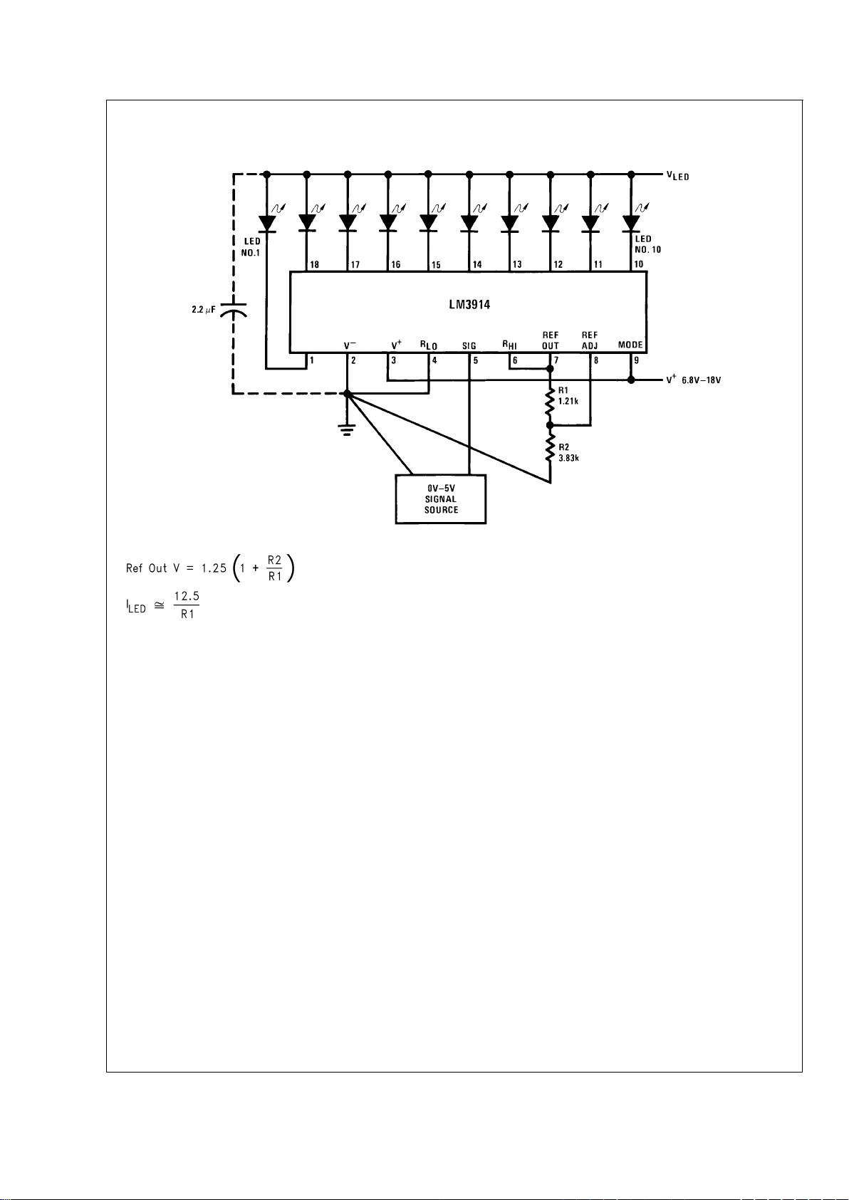
Typical Applications
0V to 5V Bar Graph Meter
DS007970-1
Note: Grounding method is typical of
all
uses. The 2.2 µF tantalum or 10 µF aluminum electrolytic capacitor is needed if leads to the LED supply are 6" or
longer.
LM3914
www.national.com 2
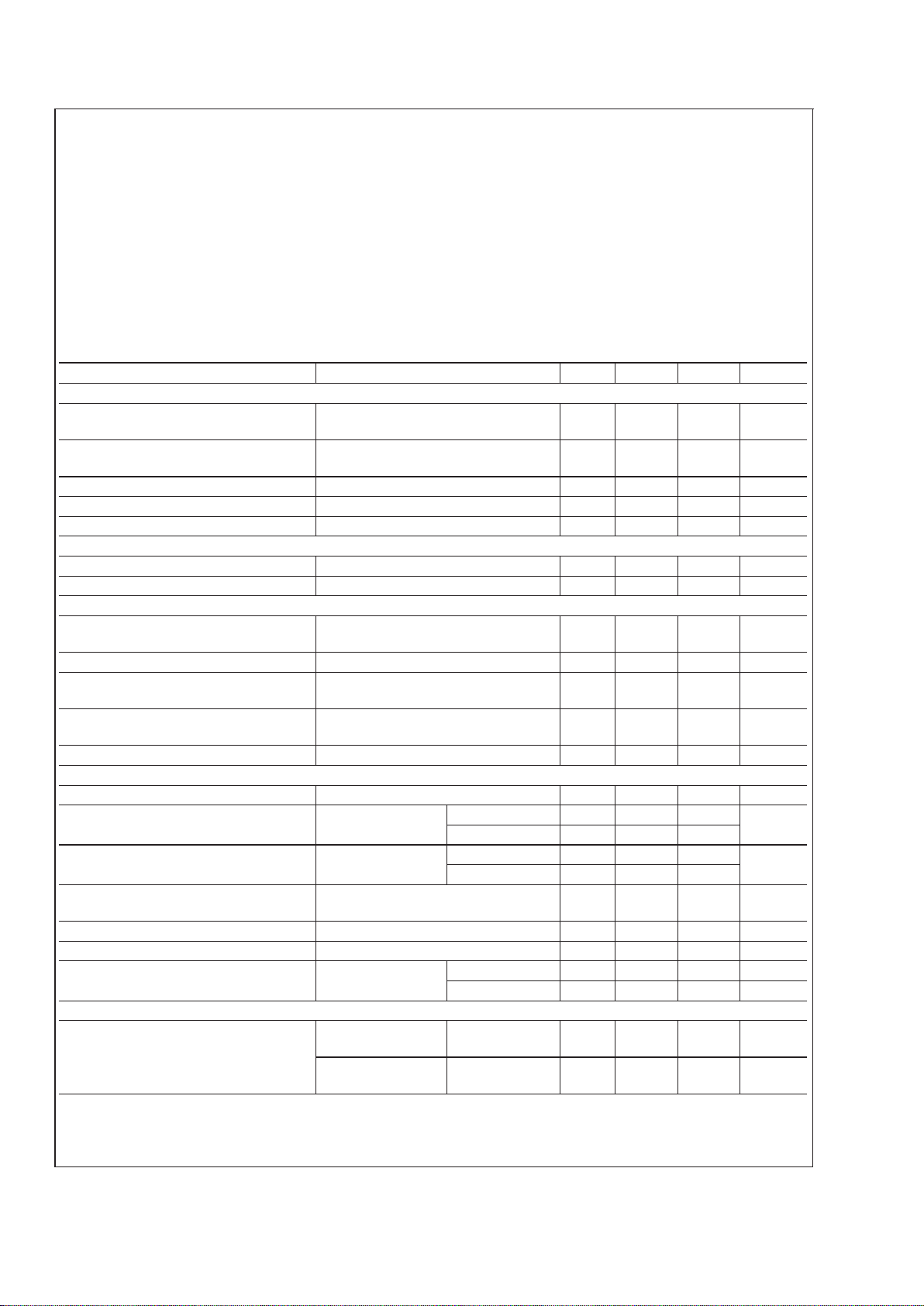
Absolute Maximum Ratings (Note 1)
If Military/Aerospace specified devices are required,
please contact the National Semiconductor Sales Office/
Distributors for availability and specifications.
Power Dissipation (Note 6)
Molded DIP (N) 1365 mW
Supply Voltage 25V
Voltage on Output Drivers 25V
Input Signal Overvoltage (Note 4)
±
35V
Divider Voltage −100 mV to V
+
Reference Load Current 10 mA
Storage Temperature Range −55˚C to +150˚C
Soldering Information
Dual-In-Line Package
Soldering (10 seconds) 260˚C
Plastic Chip Carrier Package
Vapor Phase (60 seconds) 215˚C
Infrared (15 seconds) 220˚C
See AN-450 “Surface Mounting Methods and Their Effect
on Product Reliability” for other methods of soldering
surface mount devices.
Electrical Characteristics (Notes 2, 4)
Parameter Conditions (Note 2) Min Typ Max Units
COMPARATOR
Offset Voltage, Buffer and First
Comparator
0V ≤ V
RLO
=
V
RHI
≤ 12V,
I
LED
=
1mA
310mV
Offset Voltage, Buffer and Any Other
Comparator
0V ≤ V
RLO
=
V
RHI
≤ 12V,
I
LED
=
1mA
315mV
Gain (∆I
LED
/∆VIN)I
L(REF)
=
2 mA, I
LED
=
10 mA 3 8 mA/mV
Input Bias Current (at Pin 5) 0V ≤ V
IN
≤ V+− 1.5V 25 100 nA
Input Signal Overvoltage No Change in Display −35 35 V
VOLTAGE-DIVIDER
Divider Resistance Total, Pin 6 to 4 8 12 17 kΩ
Accuracy (Note 3) 0.5 2
%
VOLTAGE REFERENCE
Output Voltage 0.1 mA ≤ I
L(REF)
≤ 4 mA,
V
+
=
V
LED
=
5V
1.2 1.28 1.34 V
Line Regulation 3V ≤ V
+
≤ 18V 0.01 0.03
%
/V
Load Regulation 0.1 mA ≤ I
L(REF)
≤ 4 mA,
V
+
=
V
LED
=
5V
0.4 2
%
Output Voltage Change with
Temperature
0˚C ≤ T
A
≤ +70˚C, I
L(REF)
=
1 mA,
V
+
=
5V
1
%
Adjust Pin Current 75 120 µA
OUTPUT DRIVERS
LED Current V
+
=
V
LED
=
5V, I
L(REF)
=
1 mA 7 10 13 mA
LED Current Difference (Between
Largest and Smallest LED Currents)
V
LED
=
5V I
LED
=
2 mA 0.12 0.4
mA
I
LED
=
20 mA 1.2 3
LED Current Regulation 2V ≤ V
LED
≤ 17V I
LED
=
2 mA 0.1 0.25
mA
I
LED
=
20 mA 1 3
Dropout Voltage I
LED(ON)
=
20 mA, V
LED
=
5V,
∆I
LED
=
2mA
1.5 V
Saturation Voltage I
LED
=
2.0 mA, I
L(REF)
=
0.4 mA 0.15 0.4 V
Output Leakage, Each Collector (Bar Mode) (Note 5) 0.1 10 µA
Output Leakage (Dot Mode)
(Note 5)
Pins 10–18 0.1 10 µA
Pin 1 60 150 450 µA
SUPPLY CURRENT
Standby Supply Current
(All Outputs Off)
V
+
=
5V,
I
L(REF)
=
0.2 mA
2.4 4.2 mA
V
+
=
20V,
I
L(REF)
=
1.0 mA
6.1 9.2 mA
Note 1: Absolute Maximum Ratings indicate limits beyond whichdamage to thedevice may occur.OperatingRatings indicate conditionsfor which thedevice is functional, but do notguarantee specific performancelimits. Electrical CharacteristicsstateDC and AC electricalspecifications under particular testconditions which guarantee specific performance limits. This assumes that the device is within the Operating Ratings. Specifications are not guaranteed for parameters where no limit is
given, however, the typical value is a good indication of device performance.
LM3914
www.national.com3
Electrical Characteristics (Notes 2, 4) (Continued)
Note 2: Unless otherwise stated, all specifications apply with the following conditions:
3V
DC
≤ V+≤ 20 V
DCVREF,VRHI,VRLO
≤ (V+− 1.5V)
3V
DC
≤ V
LED
≤ V+0V ≤ VIN≤ V+− 1.5V
−0.015V ≤ V
RLO
≤ 12 V
DCTA
=
+25˚C, I
L(REF)
=
0.2 mA, V
LED
=
3.0V, pin 9 connected to pin 3 (Bar Mode).
−0.015V ≤ V
RHI
≤ 12 V
DC
For higher power dissipations, pulse testing is used.
Note 3: Accuracy is measured referred to +10.000 V
DC
at pin 6, with 0.000 VDCat pin 4. At lower full-scale voltages, buffer and comparator offset voltage may add
significant error.
Note 4: Pin 5 input current must be limited to
±
3 mA. The addition of a 39k resistor in series with pin 5 allows±100V signals without damage.
Note 5: Bar mode results when pin 9 is within 20 mV of V
+
. Dot mode results when pin 9 is pulled at least 200 mV below V+or left open circuit. LED No. 10 (pin
10 output current) is disabled if pin 9 is pulled 0.9V or more below V
LED
.
Note 6: The maximum junction temperature of the LM3914 is 100˚C. Devices must be derated for operation at elevated temperatures. Junction to ambient thermal
resistance is 55˚C/W for the molded DIP (N package).
Definition of Terms
Accuracy: The difference between the observed threshold
voltage and the ideal threshold voltage for each comparator.
Specified and tested with 10V across the internal voltage divider so that resistor ratio matching error predominates over
comparator offset voltage.
Adjust Pin Current: Current flowing outof the reference adjust pin when the reference amplifier is in the linear region.
Comparator Gain: The ratio of the change in output current
(I
LED
) to the change in input voltage (VIN) required to pro-
duce it for a comparator in the linear region.
Dropout Voltage: The voltage measured at the current
source outputs required to make the output current fall by
10%.
Input Bias Current: Current flowing out of the signal input
when the input buffer is in the linear region.
LED Current Regulation: The change in output current
over the specified range of LED supply voltage (V
LED
)as
measured at the current source outputs.As the forward voltage of an LED does not change significantly with a small
change in forward current, this is equivalent to changing the
voltage at the LED anodes by the same amount.
Line Regulation: The average change in reference output
voltage over the specified range of supply voltage (V
+
).
Load Regulation: The change in reference output voltage
(V
REF
) over the specified range of load current (I
L(REF)
).
Offset Voltage: The differential input voltage which must be
applied toeach comparator tobias the outputin the linearregion. Most significant error when the voltage across the internal voltage divider is small. Specified and tested with pin
6 voltage (V
RHI
) equal to pin 4 voltage (V
RLO
).
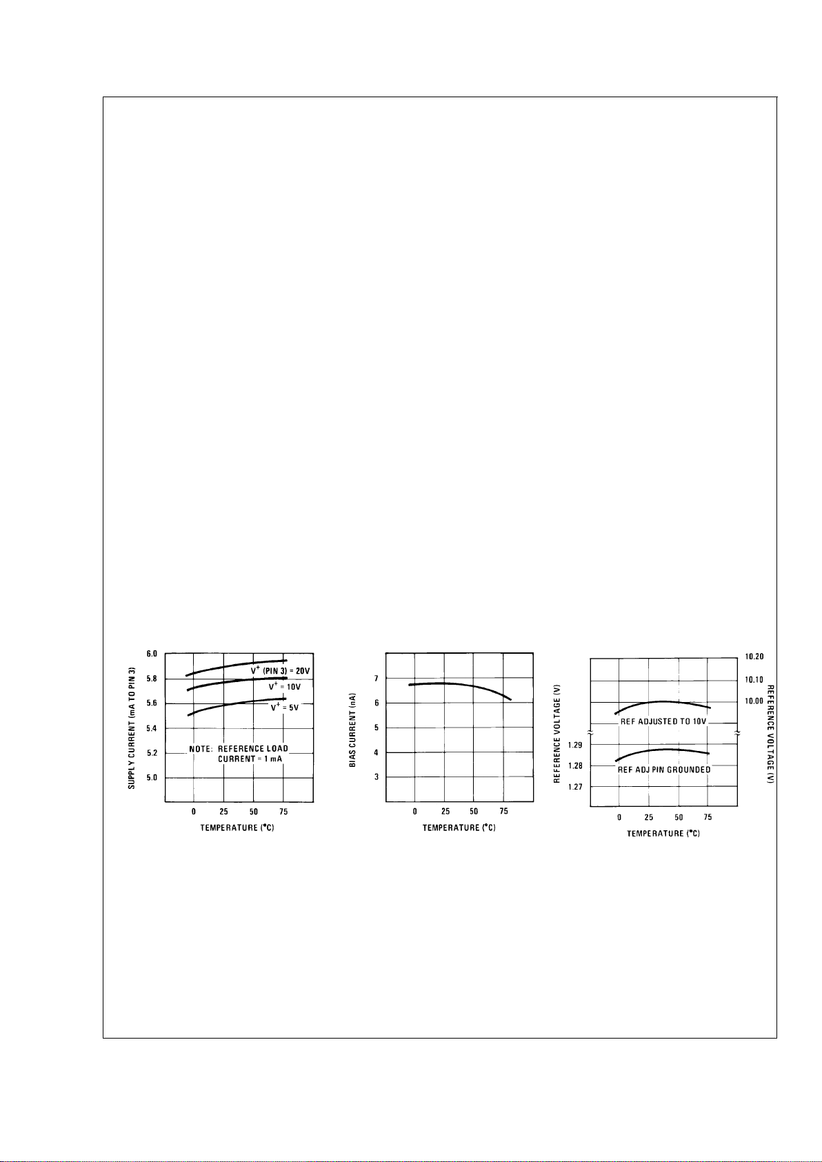
Typical Performance Characteristics
Supply Current vs
Temperature
DS007970-2
Operating Input Bias
Current vs Temperature
DS007970-20
Reference Voltage vs
Temperature
DS007970-21
LM3914
www.national.com 4
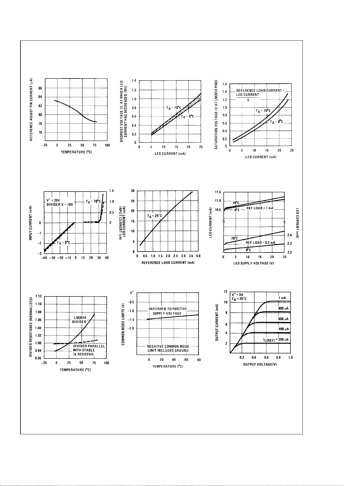
Typical Performance Characteristics (Continued)
Reference Adjust Pin
Current vs Temperature
DS007970-22
LED Current-Regulation
Dropout
DS007970-23
LED Driver Saturation
Voltage
DS007970-24
Input Current Beyond
Signal Range (Pin 5)
DS007970-25
LED Current vs
Reference Loading
DS007970-26
LED Driver Current
Regulation
DS007970-27
Total Divider Resistance
vs Temperature
DS007970-28
Common-Mode Limits
DS007970-29
Output Characteristics
DS007970-30
LM3914
www.national.com5
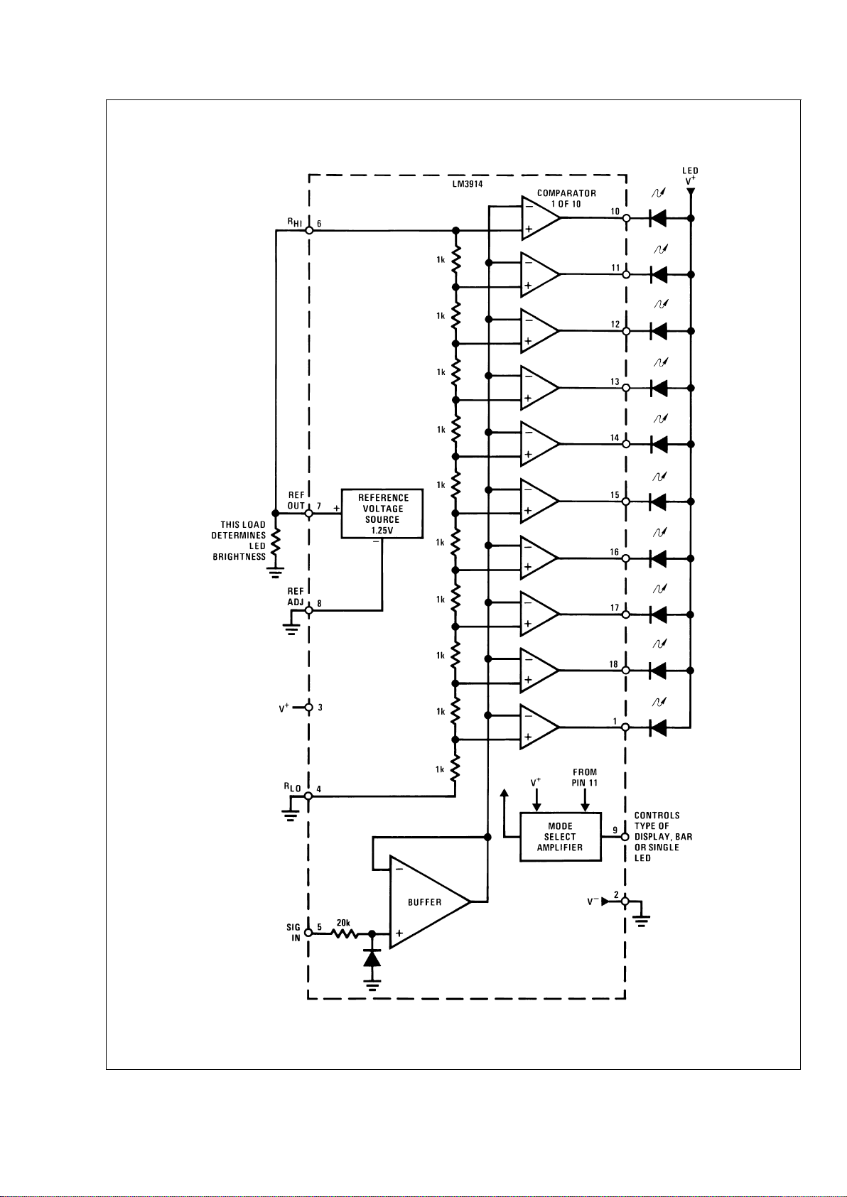
Block Diagram (Showing Simplest Application)
DS007970-3
LM3914
www.national.com 6
 Loading...