

NSC LM390N Datasheet
LM390 1W Battery Operated Audio Power Amplifier
Y
General Description
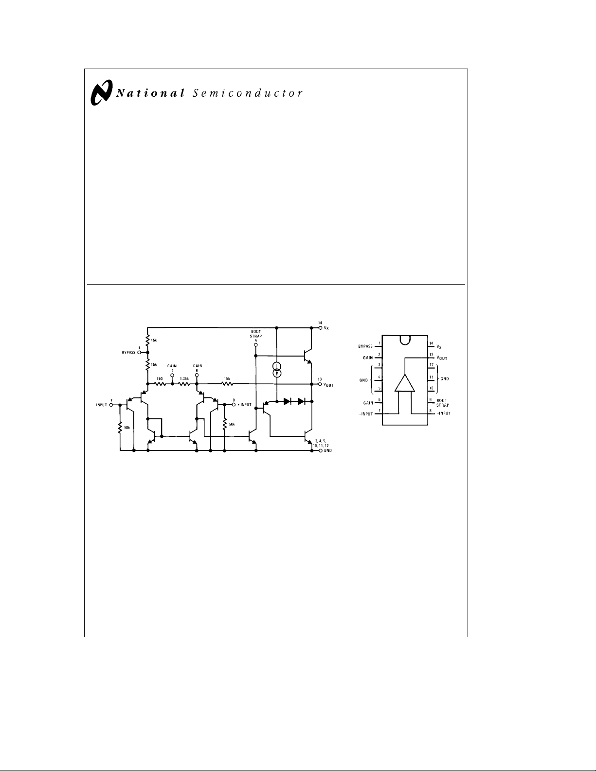
The LM390 Power Audio Amplifier is optimized for 6V, 7.5V,
9V operation into low impedance loads. The gain is internally set at 20 to keep the external part count low, but the
addition of an external resistor and capacitor between pins
2 and 6 wil increase the gain to any value up to 200. The
inputs are ground referenced while the output is automatically biased to one half the supply voltage.
Features
Y
Battery operation
Y
1W output power
Y
Minimum external parts
Y
Excellent supply rejection
Y
Ground referenced input
Equivalent Schematic and Connection Diagrams
Self-centering output quiescent voltage
Y
Variable voltage gain
Y
Low distortion
Y
Fourteen pin dual-in-line package
Applications
Y
AM-FM radio amplifiers
Y
Portable tape player amplifiers
Y
Intercoms
Y
TV sound systems
Y
Lamp drivers
Y
Line drivers
Y
Ultrasonic drivers
Y
Small servo drivers
Y
Power converters
Dual-In-Line Package
LM390 1W Battery Operated Audio Power Amplifier
April 1995
Order Number LM390N
TL/H/7848– 2
See NS Package Number N14A
TL/H/7848– 1
C
1995 National Semiconductor Corporation RRD-B30M115/Printed in U. S. A.
TL/H/7848
Absolute Maximum Ratings
If Military/Aerospace specified devices are required,
please contact the National Semiconductor Sales
Office/Distributors for availability and specifications.
Supply Voltage 10V
Package Dissipation 14-Pin DIP (Note 1) 8.3W
Input Voltage
Storage Temperature
b
65§Ctoa150§C
g
0.4V
Operating Temperature 0
Ctoa70§C
§
Junction Temperature 150§C
Lead Temperature (Soldering, 10 sec.) 260§C
Thermal Resistance
i
JC
i
JA
30§C/W
79§C/W
Electrical Characteristics T
e
25§C,
A
(Figure 1)
Symbol Parameter Conditions Min Typ Max Units
V
S
I
Q
P
OUT
A
V
BW Bandwidth V
THD Total Harmonic Distortion V
PSRR Power Supply Rejection Ratio V
Operating Supply Voltage 4 9 V
Quiescent Current V
Output Power V
Voltage Gain V
e
S
e
S
e
S
10 mF from Pin 2 to 6 46 dB
e
S
e
S
e
1 kHz, Pins 2 and 6 Open
f
e
S
Pins 2 and 6 Open, Referred to Output 50 dB
e
6V, V
6V, R
01020mA
IN
e
4X, THDe10% 0.8 1.0 W
L
6V, fe1 kHz 23 26 30 dB
6V, Pins 2 and 6 Open 300 kHz
e
6V, R
4X,P
L
6V, fe1 kHz, C
OUT
BYPASS
e
500 mW
e
0.2 1 %
10 mF,
(Note 2)
R
IN
I
BIAS
Note 1: Pins 3, 4, 5, 10, 11, 12 at 25§C. Above 25§C case, derate at 15§C/W junction to case, or 85§C/W junction to ambient.
Note 2: If load and bypass capacitor are returned to V
Input Resistance 10 50 kX
(Figure 2)
S
e
6V, Pins 7 and 8 Open 250 nA
S
, rather than ground
(Figure 1)
, PSRR is typically 30 dB.
Input Bias Current V
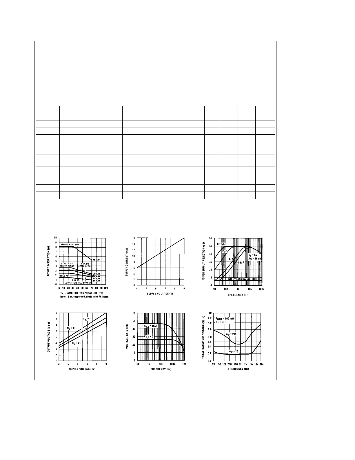
Typical Performance Characteristics
Maximum Device Dissipation
vs Ambient Temperature
Quiescent Supply Current vs
Supply Voltage
Power Supply Rejection Ratio
(Referred to the Output) vs
Frequency
Peak-to-Peak Output Voltage
Swing vs Supply Voltage
Voltage Gain vs Frequency Distortion vs Frequency
TL/H/7848– 5
2
 Loading...