NSC LM389N Datasheet

LM389 Low Voltage Audio Power Amplifier
with NPN Transistor Array
Y
General Description
The LM389 is an array of three NPN transistors on the same
substrate with an audio power amplifier similar to the
LM386.
The amplifier inputs are ground referenced while the output
is automatically biased to one half the supply voltage. The
gain is internally set at 20 to minimize external parts, but the
addition of an external resistor and capacitor between pins
4 and 12 will increase the gain to any value up to 200.
The three transistors have high gain and excellent matching
characteristics. They are well suited to a wide variety of applications in DC through VHF systems.
Features
Amplifier
Y
Battery operation
Y
Minimum external parts
Y
Wide supply voltage range
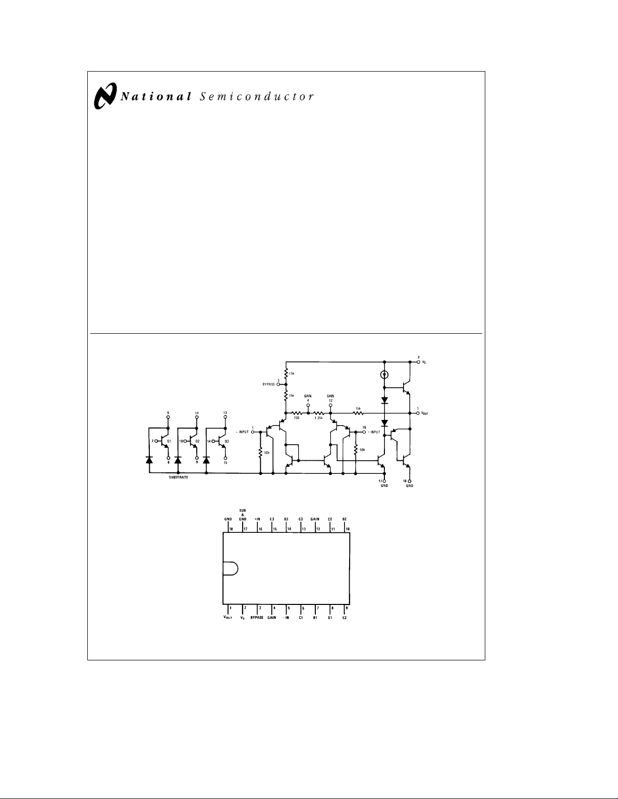
Equivalent Schematic and Connection Diagrams
Low quiescent current drain
Y
Voltage gains from 20 to 200
Y
Ground referenced input
Y
Self-centering output quiescent voltage
Y
Low distortion
Transistors
Y
Operation from 1 mAto25mA
Y
Frequency range from DC to 100 MHz
Y
Excellent matching
Applications
Y
AM-FM radios
Y
Portable tape recorders
Y
Intercoms
Y
Toys and games
Y
Walkie-talkies
Y
Portable phonographs
Y
Power converters
LM389 Low Voltage Audio Power Amplifier with NPN Transistor Array
December 1994
TL/H/7847– 1
Dual-In-Line Package
Order Number LM389N
TL/H/7847– 2
See NS Package Number N18A
C
1995 National Semiconductor Corporation RRD-B30M115/Printed in U. S. A.
TL/H/7847

Absolute Maximum Ratings
If Military/Aerospace specified devices are required,
please contact the National Semiconductor Sales
Office/Distributors for availability and specifications.
Supply Voltage 15V
Package Dissipation (Note 1) 1.89W
Ctoa70§C
§
e
25§C
A
g
0.4V
§
§
12V
Input Voltage
Storage Temperature
b
65§Ctoa150§C
Operating Temperature 0
Junction Temperature 150
Lead Temperature (Soldering, 10 sec.) 260
Collector to Emitter Voltage, V
CEO
Electrical Characteristics T
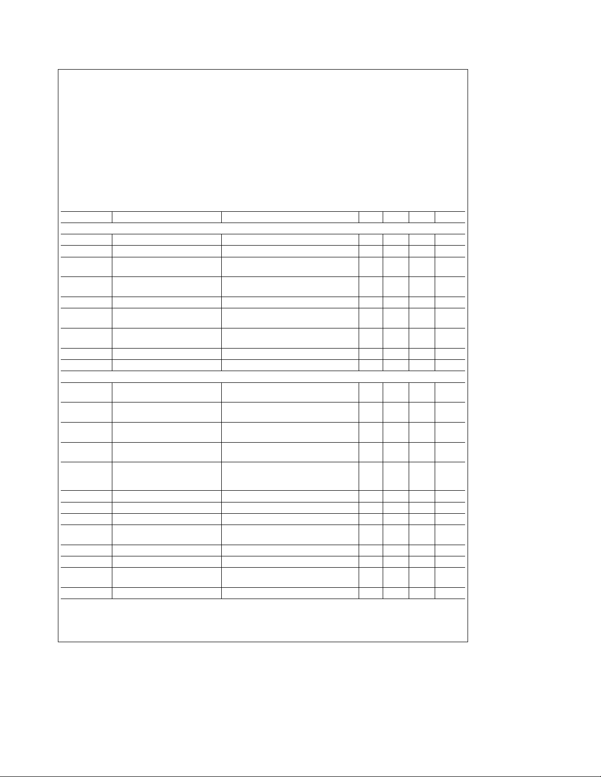
Symbol Parameter Conditions Min Typ Max Units
AMPLIFIER
V
S
I
Q
P
OUT
A
V
BW Bandwidth V
THD Total Harmonic Distortion V
PSRR Power Supply Rejection Ratio V
R
IN
I
BIAS
Operating Supply Voltage 4 12 V
Quiescent Current V
Output Power (Note 3)
Voltage Gain V
e
S
e
THD
e
S
10 mF from Pins 4 to 12 46 dB
e
S
e
S
e
1 kHz, Pins 4 and 12 Open
f
e
S
Pins 4 and 12 Open, Referred to Output
Input Resistance 10 50 kX
Input Bias Current V
e
S
TRANSISTORS
V
CEO
V
CBO
V
CIO
V
EBO
H
FE
h
oe
V
BE
V
l
BE1–VBE2
V
CESAT
C
EB
C
CB
C
CI
h
fe
Note 1: For operation in ambient temperatures above 25§C, the device must be derated based on a 150§C maximum junction temperature and a thermal resistance
C/W junction to ambient.
of 66
§
Note 2: The collector of each transistor is isolated from the substrate by an integral diode. Therefore, the collector voltage should remain positive with respect to
pin 17 at all times.
Note 3: If oscillation exists under some load conditions, add 2.7X and 0.05 m F series network from pin 1 to ground.
Collector to Emitter I
Breakdown Voltage
Collector to Base I
Breakdown Voltage
Collector to Substrate I
Breakdown Voltage
Emitter to Base I
Breakdown Voltage
Static Forward Current I
Transfer Ratio (Static Beta) I
Open-Circuit Output Admittance I
Base to Emitter Voltage I
Base to Emitter Voltage Offset I
l
Collector to Emitter I
Saturation Voltage
Emitter to Base Capacitance V
Collector to Base Capacitance V
Collector to Substrate V
Capacitance
High Frequency Current Gain I
e
1 mA, I
C
e
10 mA, I
C
e
10 mA, I
C
e
10 mA, I
E
e
10 mA 100
C
e
1 mA 100 275
C
e
10 mA 275
I
C
e
1 mA, V
C
e
1 mA 0.7 0.85 V
E
e
1mA 1 5 mV
E
e
10 mA, I
C
e
EB
e
CB
e
CI
e
10 mA, V
C
Collector to Base Voltage, V
Collector to Substrate Voltage, V
(Note 2) 15V
Collector Current, I
Emitter Current, I
Base Current, I
Power Dissipation (Each Transistor) T
B
Thermal Resistance
C
C
6V, V
i
JC
i
JA
e
0V 6 12 mA
IN
10%
e
6V, R
V
S
e
9V, R
V
S
E
L
L
CBO
CIO
C
s
a
70§C 150 mW
A
e
8X 250 325 mW
e
16X 500 mW
25 mA
25 mA
5mA
24§C/W
70§C/W
6V, fe1 kHz 23 26 30 dB
6V, Pins 4 and 12 Open 250 kHz
e
6V, R
8X,P
L
6V, fe1 kHz, C
OUT
BYPASS
e
125 mW,
e
10 mF,
0.2 3.0 %
30 50 dB
6V, Pins 5 and 16 Open 250 nA
e
0
B
e
0
E
e
e
I
E
C
CE
B
0
B
e
0
e
5V, fe1.0 kHz 20 mmho
e
1mA
12 20 V
15 40 V
15 40 V
6.4 7.1 7.8 V
0.15 0.5 V
3V 1.5 pF
3V 2 pF
3V
e
5V, fe100 MHz 1.5 5.5
CE
3.5 pF
2
15V

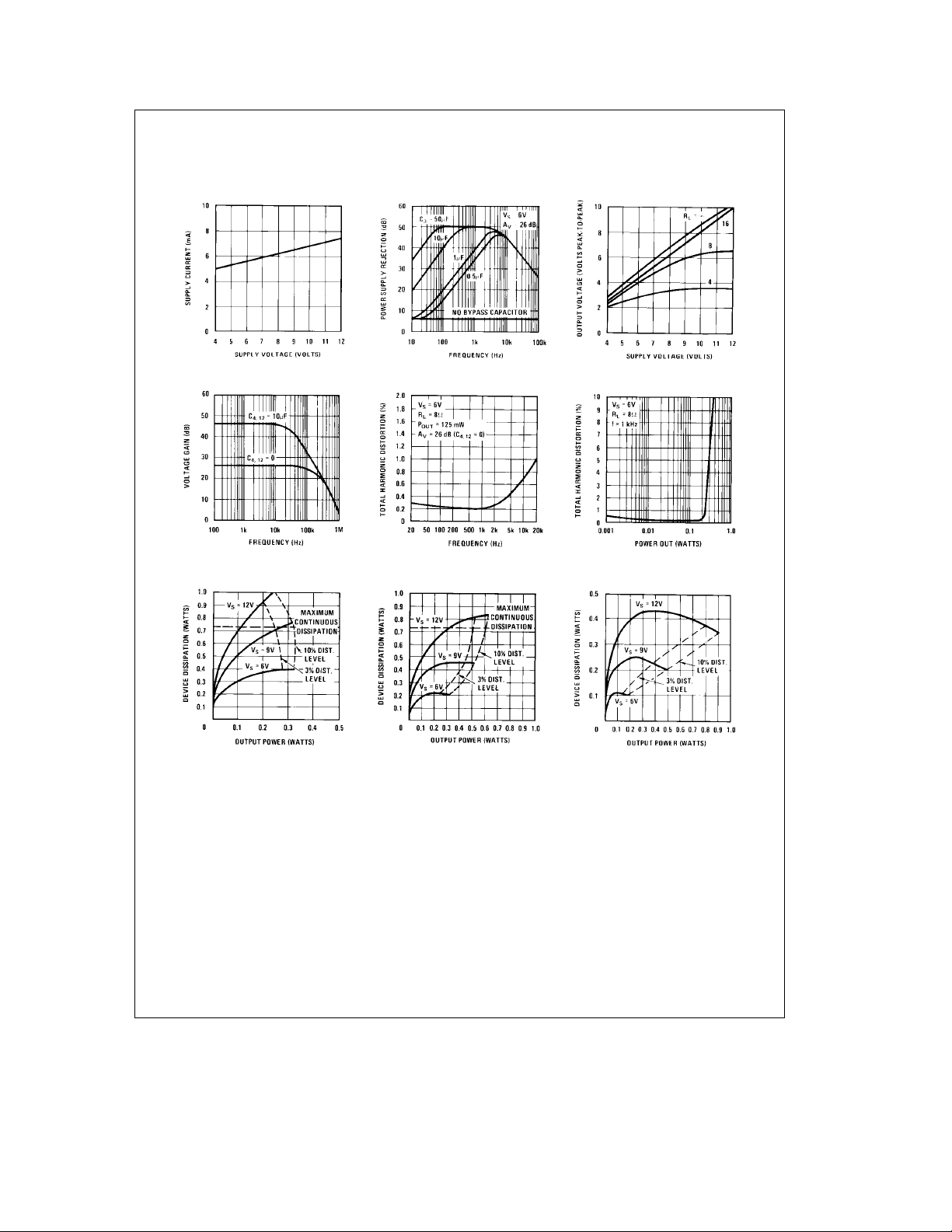
Typical Amplifier Performance Characteristics
Quiescent Supply Current
vs Supply Voltage
Voltage Gain vs Frequency Distortion vs Frequency Distortion vs Output Power
Device Dissipation vs Output
PowerÐ4X Load
Power Supply Rejection Ratio
(Referred to the Output)
vs Frequency
Device Dissipation vs Output
PowerÐ8X Load
Peak-to-Peak Output Voltage
Swing vs Supply Voltage
Device Dissipation vs Output
PowerÐ16X Load
TL/H/7847– 3
3
 Loading...