

LM388 1.5W Audio Power Amplifier
Y
General Description
The LM388 is an audio amplifier designed for use in medium
power consumer applications. The gain is internally set to
20 to keep external part count low, but the addition of an
external resistor and capacitor between pins 2 and 6 will
increase the gain to any value up to 200.
The inputs are ground referenced while the output is automatically biased to one half the supply voltage.
Features
Y
Minimum external parts
Y
Wide supply voltage range
Y
Excellent supply rejection
Y
Ground referenced input
Y
Self-centering output quiescent voltage
Variable voltage gain
Y
Low distortion
Y
Fourteen pin dual-in-line package
Y
Low voltage operation, 4V
Applications
Y
AM-FM radio amplifiers
Y
Portable tape player amplifiers
Y
Intercoms
Y
TV sound systems
Y
Lamp drivers
Y
Line drivers
Y
Ultrasonic drivers
Y
Small servo drivers
Y
Power converters
LM388 1.5W Audio Power Amplifier
February 1995
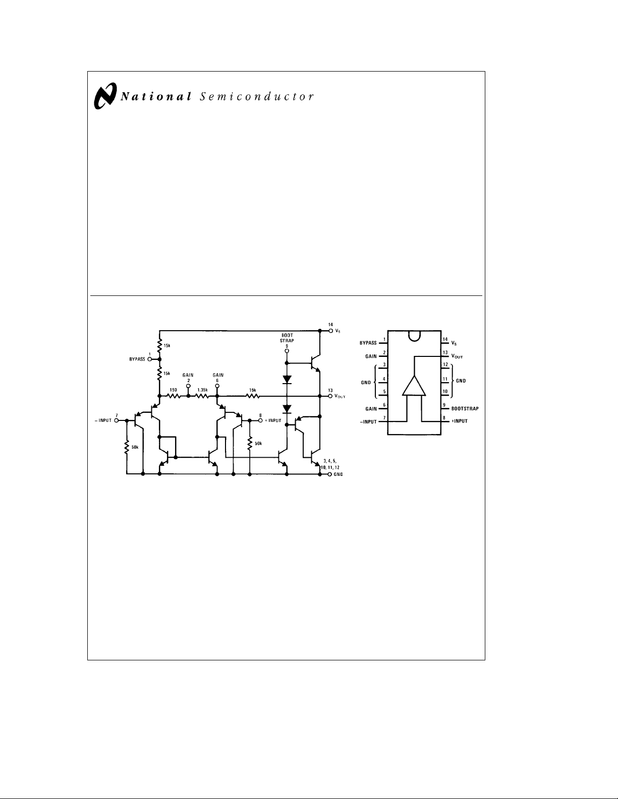
Equivalent Schematic and Connection Diagrams
TL/H/7846– 1
Dual-In-Line Package
TL/H/7846– 2
Top View
Order Number LM388N-1
See NS Package Number N14A
C
1995 National Semiconductor Corporation RRD-B30M115/Printed in U. S. A.
TL/H/7846
Absolute Maximum Ratings
If Military/Aerospace specified devices are required,
please contact the National Semiconductor Sales
Office/Distributors for availability and specifications.
Supply Voltage 15V
Package Dissipation 14-Pin DIP (Note 1) 8.3W
Input Voltage
Storage Temperature
b
65§Ctoa150§C
g
0.4V
Operating Temperature 0
Ctoa70§C
§
Junction Temperature 150§C
Lead Temperature (Soldering, 10 sec.) 260§C
Thermal Resistance
i
JC
i
JA
30§C/W
79§C/W
Electrical Characteristics T
e
25§C,
A
(Figure 1)
Symbol Parameter Conditions Min Typ Max Units
V
S
I
Q
P
OUT
A
V
BW Bandwidth V
THD Total Harmonic Distortion V
PSRR Power Supply Rejection Ratio V
R
IN
I
BIAS
Note 1: Pins 3, 4, 5, 10, 11, 12 at 25§C. Derate at 15§C/W above 25§C case.
Note 2: The amplifier should be in high gain for full swing on higher supplies due to input voltage limitations.
Note 3: If load and bypass capacitor are returned to V
Operating Supply Voltage
LM388
Quiescent Current V
LM388 V
e
0
IN
e
12V
S
412V
16 23 mA
Output Power (Note 2) R1eR2e180X, THDe10%
LM388N-1 V
Voltage Gain V
(Note 3) Pins 2 and 6 Open, Referred to Output
e
S
e
V
S
e
S
10 mF from Pins 2 to 6 46 dB
e
S
e
S
fe1 kHz, Pins 2 and 6 Open
e
S
e
12V, R
6V, R
8X 1.5 2.2 W
L
e
4X 0.6 0.8 W
L
12V, fe1 kHz 23 26 30 dB
12V, Pins 2 and 6 Open 300 kHz
e
12V, R
8X,P
L
12V, fe1 kHz, C
OUT
BYPASS
e
500 mW,
e
10 mF,
0.1 1 %
50 dB
Input Resistance 10 50 kX
(Figure 2),
S
e
12V, Pins 7 and 8 Open 250 nA
S
rather than ground
(Figure 1),
PSRR is typically 30 dB.
Input Bias Current V
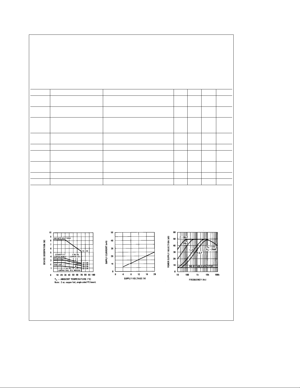
Typical Performance Characteristics
Maximum Device Dissipation vs
Ambient Temperature
Quiescent Supply Current vs
Supply Voltage
Power Supply Rejection Ratio
(Referred to the Output) vs
Frequency
TL/H/7846– 5
2
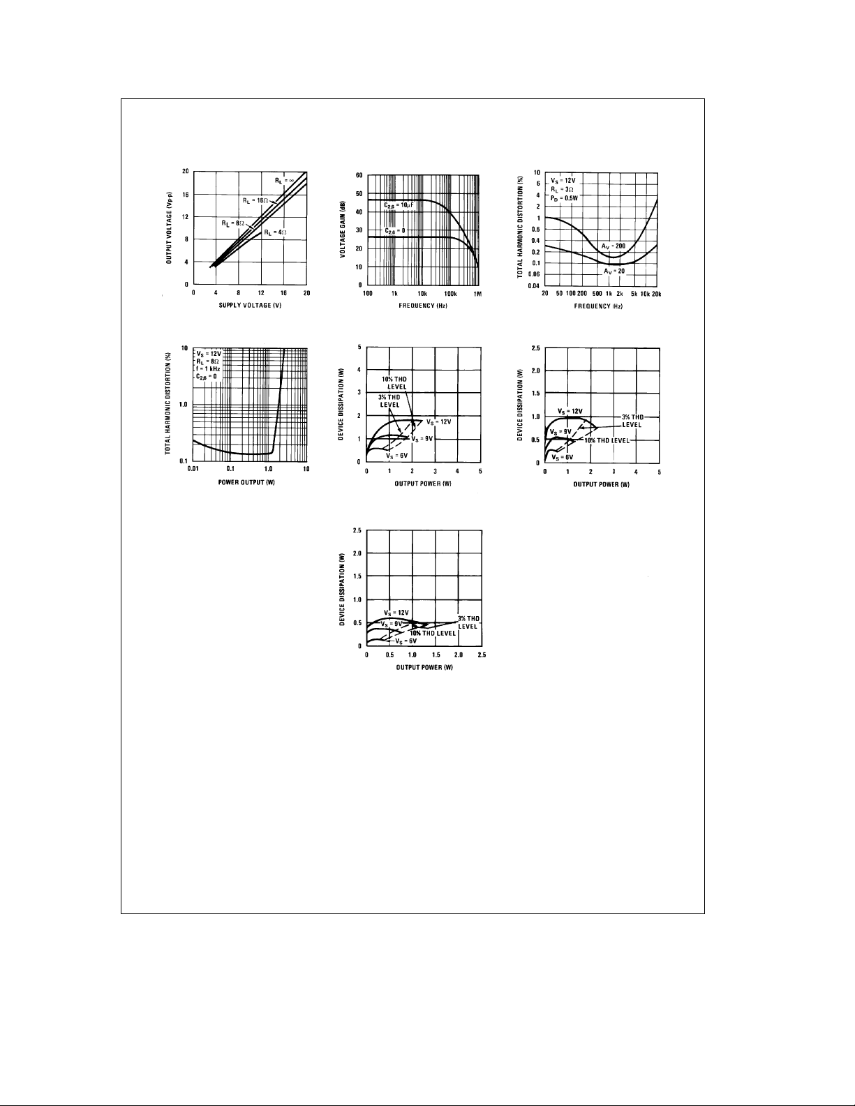
Typical Performance Characteristics (Continued)
Peak-to-Peak Output Voltage
Swing vs Supply Voltage
Voltage Gain vs Frequency Distortion vs Frequency
Distortion vs Output Power PowerÐ4X Load
Device Dissipation vs Output
Device Dissipation vs
Output PowerÐ16X Load
Application Hints
GAIN CONTROL
To make the LM388 a more versatile amplifier, two pins (2
and 6) are provided for gain control. With pins 2 and 6 open,
the 1.35 kX resistor sets the gain at 20 (26 dB). If a capacitor is put from pins 2 to 6, bypassing the 1.35 kX resistor,
the gain will go up to 200 (46 dB). If a resistor is placed in
series with the capacitor, the gain can be set to any value
from 20 to 200. A low frequency pole in the gain response is
caused by the capacitor working against the external resistor in series with the 150X internal resistor. If the capacitor
is eliminated and a resistor connects pins 2 to 6 then the
Device Dissipation vs
Output PowerÐ8X Load
TL/H/7846– 6
output dc level may shift due to the additional dc gain. Gain
control can also be done by capacitively coupling a resistor
(or FET) from pin 6 to ground, as in
Additional external components can be placed in parallel
with the internal feedback resistors to tailor the gain and
frequency response for individual applications. For example,
we can compensate poor speaker bass response by frequency shaping the feedback path. This is done with a series RC from pin 6 to 13 (paralleling the internal 15 kX resistor). For 6 dB effective bass boost: Rj15 kX, the lowest
value for good stable operation is R
Figure 7
e
.
10 kX if pin 2
3
 Loading...