NSC LM3880MFX-1AD, LM3880 Datasheet

March 2007
LM3880
Power Sequencer
General Description
The LM3880 Power Sequencer offers the easiest method to
control power up and power down of multiple power supplies
(switchers or linear regulators). By staggering the startup sequence, it is possible to avoid latch conditions or large in-rush
currents that can affect the reliability of the system.
Available in a SOT23-6 package, the Power Sequencer contains a precision enable pin and three open drain output flags.
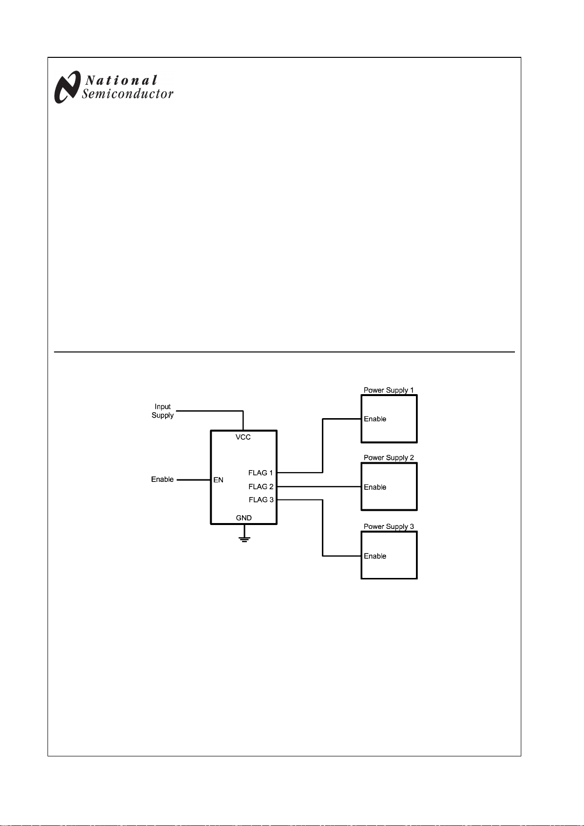
Upon enabling the LM3880 the three output flags will sequentially release, after individual time delays, permitting the connected power supplies to startup. The output flags will follow
a reverse sequence during power down to avoid latch conditions.
Standard timing option of 30ms is available.
EPROM capability allows every delay and sequence to be
fully adjustable. Contact National Semiconductor if a nonstandard configuration is required.
Features
■
Easiest method to sequence rails
■
Power up and power down control
■
Input voltage range of 2.7V to 5.5V
■
Small footprint SOT23-6
■
Low quiescent current of 25 µA
■
Standard timing options available
■
Customization of timing and sequence available through
factory programmability
Applications
■
Multiple supply sequencing
■
Microprocessor / Microcontroller sequencing
■
FPGA sequencing
Typical Application Circuit
20192601
© 2007 National Semiconductor Corporation 201926 www.national.com
LM3880 Power Sequencer

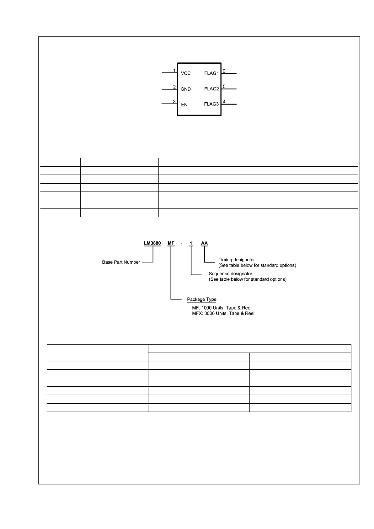
Connection Diagram
20192602
Top View
SOT23–6 Package
Pin Descriptions
Pin # Name Function
1 VCC Input supply
2 GND Ground
3 EN Precision enable pin
4 FLAG3 Open drain output #3
5 FLAG2 Open drain output #2
6 FLAG1 Open drain output #1
Ordering Information
20192603
Sequence Designator Table
Sequence Number Flag Order
Power Up Power Down
1 1 - 2 - 3 3 - 2 - 1
2 1 - 2 - 3 3 - 1 - 2
3 1 - 2 - 3 2 - 3 - 1
4 1 - 2 - 3 2 - 1 - 3
5 1 - 2 - 3 1 - 3 - 2
6 1 - 2 - 3 1 - 2 - 3
See timing diagrams for more information
www.national.com 2
LM3880

Timing Designator Table
Timing
Designator
t
d1
t
d2
t
d3
t
d4
t
d5
t
d6
AA 10ms 10ms 10ms 10ms 10ms 10ms
AB 30ms 30ms 30ms 30ms 30ms 30ms
AC 60ms 60ms 60ms 60ms 60ms 60ms
AD 120ms 120ms 120ms 120ms 120ms 120ms
See timing diagrams for more information
LM3880 Ordering Information
Order
Number
Timer settings Sequence
Order
Supplied As
Package
Type
NSC
Package
Drawing
Package
Marking
t
d1
t
d2
t
d3
t
d4
t
d5
t
d6
LM3880
MF-1AA
10ms 10ms 10ms 10ms 10ms 10ms 1 1k units T&R
SOT23-6 MF06A
F20A
LM3880
MFX-1AA
10ms 10ms 10ms 10ms 10ms 10ms 1 3k units T&R F20A
LM3880
MF-1AB
30ms 30ms 30ms 30ms 30ms 30ms 1 1k units T&R F21A
LM3880
MFX-1AB
30ms 30ms 30ms 30ms 30ms 30ms 1 3k units T&R F21A
LM3880
MF-1AC
60ms 60ms 60ms 60ms 60ms 60ms 1 1k units T&R F22A
LM3880
MFX-1AC
60ms 60ms 60ms 60ms 60ms 60ms 1 3k units T&R F22A
LM3880
MF-1AD
120ms 120ms 120ms 120ms 120ms 120ms 1 1k units T&R F23A
LM3880
MFX-1AD
120ms 120ms 120ms 120ms 120ms 120ms 1 3k units T&R F23A
Non-standard parts are available upon request. Please contact National Semiconductor for more information.
3 www.national.com
LM3880

Absolute Maximum Ratings (Note 1)
If Military/Aerospace specified devices are required,
please contact the National Semiconductor Sales Office/
Distributors for availability and specifications.
VCC −0.3V to +6.0V
EN, FLAG1, FLAG2, FLAG3 −0.3V to 6.0V
Max Flag 'ON' Current 50 mA
Storage Temperature Range −65°C to +150°C
Junction Temperature 150°C
Lead Temperature (Soldering, 5
sec.) 260°C
Minimum ESD Rating ±2 kV
Operating Ratings (Note 1)
VCC to GND 2.7V to 5.5V
EN, FLAG1, FLAG2, FLAG3 −0.3V to VCC + 0.3V
Junction Temperature −40°C to +125°C
Electrical Characteristics Specifications with standard typeface are for T
J
= 25°C, and those in bold face type
apply over the full Operating Temperature Range (TJ = -40°C to +125°C). Minimum and Maximum limits are guaranteed through
test, design or statistical correlation. Typical values represent the most likely parametric norm at TJ = 25°C and are provided for
reference purposes only. Unless otherwise specified VCC = 3.3V.
Symbol Parameter Conditions Min
(Note 3)
Typ
(Note 4)
Max
(Note 3)
Unit
I
Q
Operating Quiescent current 25 80 µA
Open Drain Flags
I
FLAG
FLAGx Leakage Current V
FLAGx
= 3.3V 1 20 nA
V
OL
FLAGx Output Voltage Low I
FLAGx
= 1.2mA 0.4 V
Power Up Sequence
t
d1
Timer delay 1 accuracy -15 15 %
t
d2
Timer delay 2 accuracy -15 15 %
t
d3
Timer delay 3 accuracy -15 15 %
Power Down Sequence
t
d4
Timer delay 4 accuracy -15 _ 15 %
t
d5
Timer delay 5 accuracy -15 15 %
t
d6
Timer delay 6 accuracy -15 15 %
Timing Delay Error
(t
d(x)
– 400 us) / t
d(x+1)
Ratio of timing delays For x = 1 or 4 95 105 %
t
d(x)
/ t
d(x+1)
Ratio of timing delays For x = 2 or 5 95 105 %
ENABLE Pin
V
EN
EN pin threshold 1.0 1.25 1.4 V
I
EN
EN pin pull-up current VEN = 0V 7 µA
Note 1: Absolute Maximum Ratings indicate limits beyond which damage to the device may occur. Operating Ratings indicate conditions for which the device is
intended to be functional, but does not guarantee specific performance limits. For guaranteed specifications and conditions, see the Electrical Characteristics.
Note 2: The human body model is a 100 pF capacitor discharged through a 1.5 kΩ resistor into each pin.
Note 3: Limits are 100% production tested at 25°. Limits over the operating temperature range are guaranteed through correlation using Statistical Quality Control
(SQC) methods. The limits are used to calculate National's Average Outgoing Quality Level (AOQL).
Note 4: Typical numbers are at 25°C and represent the most likely parametric norm.
www.national.com 4
LM3880
 Loading...