NSC LM3880EVAL Datasheet

LM3880 Power Sequencer
Demo Board
National Semiconductor
Application Note 1491
Chance Dunlap
November 2006
Introduction
The LM3880 evaluation board has been designed to permit
the designer to connect it directly to the power supplies of an
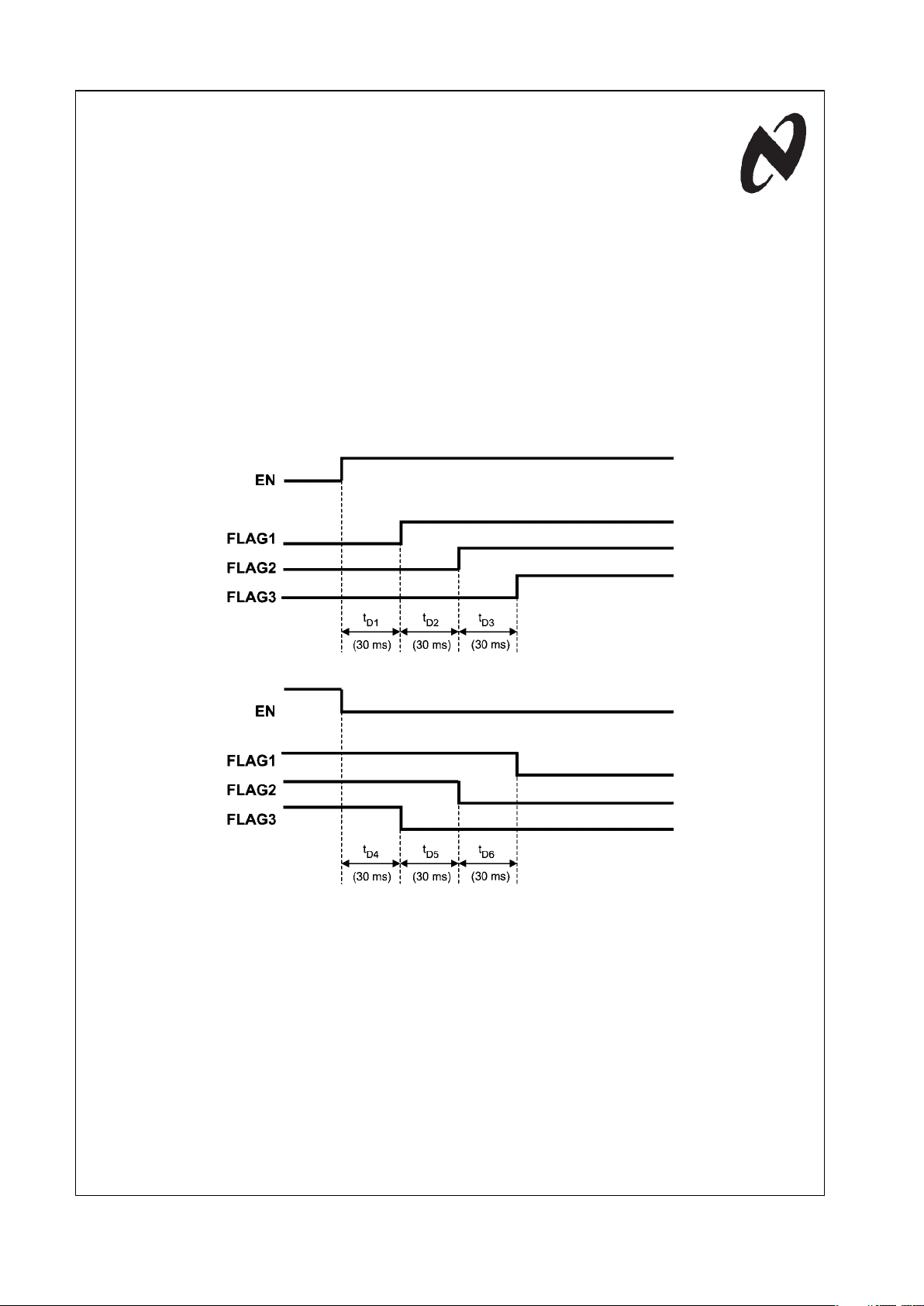
existing system to enable sequencing. Upon enabling the device the three open drain output flags will rise in sequential
order, 1-2-3. Once the part is disabled, the shutdown sequence will occur in reverse order 3-2-1. Therefore the last
power supply that started up, will be the first to shutdown. The
evaluation board contains the LM3880MF-1-AB device which
has been factory set, so that each time delay between flags
will be 30ms. Several different timing options are available as
standard off the shelf parts, but if a custom timing or shutdown
sequence is needed please contact National Semiconductor.
The LM3880 has an internal EPROM that can be factory programmed to allow almost any sequencing combination to
occur. Please refer to the datasheet for programming possibilities.
Timing Sequence
The LM3880 demoboard timing sequence of the output flags
is shown below:
20196301
20196302
© 2006 National Semiconductor Corporation 201963 www.national.com
LM3880 Power Sequencer Demo Board AN-1491

Schematic
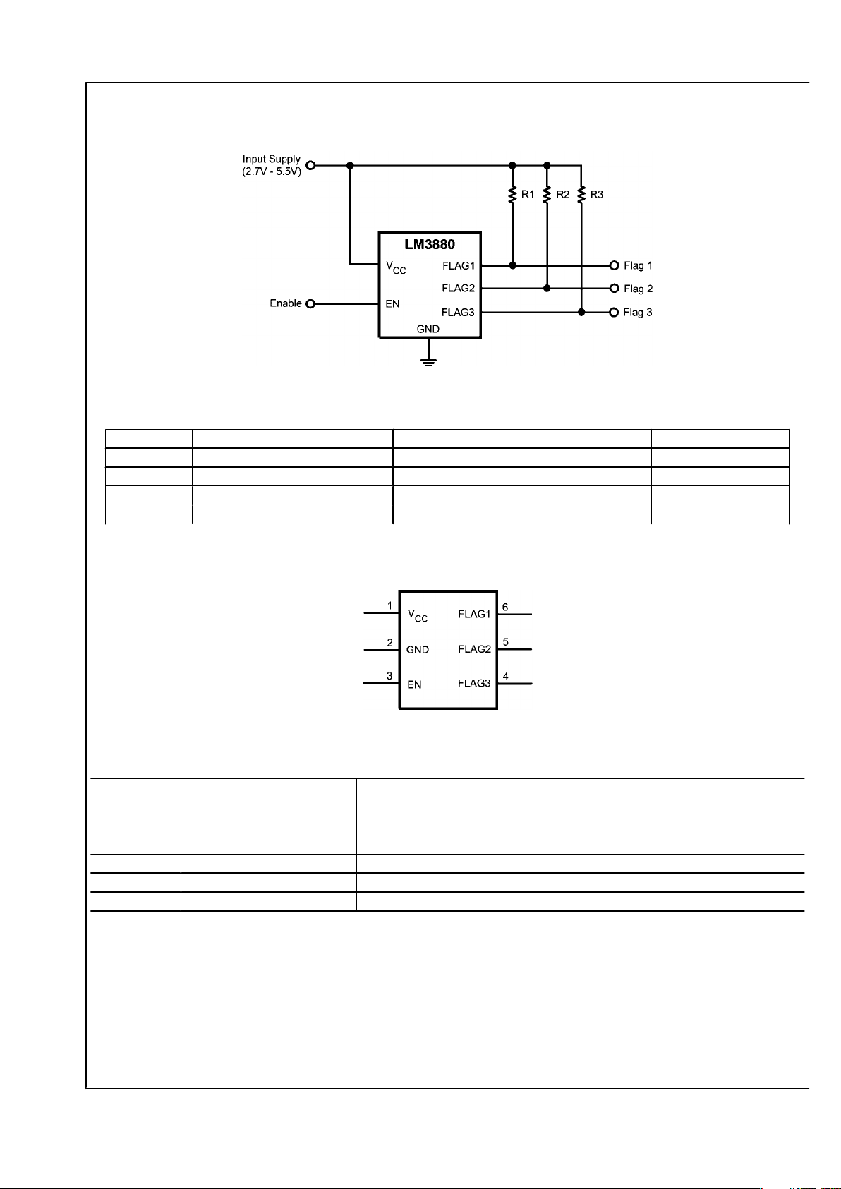
The LM3880 demoboard has been designed with the pullup
resistors on board to permit connection to an enable pin of a
switcher. The demoboard can accommodate an input voltage
from +2.7V to +5.5V.
20196303
Bill of Materials
Designator Description Part # Quantity Manufacturer
U1 LM3880, Sequence 1, 30ms timing LM3880MF-1-AB 1 NSC
R1 100K Resistor, 0603 CRCW0603100KFKEA 1 Vishay
R2 100K Resistor, 0603 CRCW0603100KFKEA 1 Vishay
R3 100K Resistor, 0603 CRCW0603100KFKEA 1 Vishay
Pin-Out
The pin-out and pin description of the LM3880 is shown below.
20196304
Pin Descriptions
Pin # Name Function
1 VCC Input supply
2 GND Ground
3 EN Precision enable pin
4 FLAG3 Open drain output #3
5 FLAG2 Open drain output #2
6 FLAG1 Open drain output #1
www.national.com 2
AN-1491
 Loading...