

NSC LM3876TF, LM3876T, LM3876DWF Datasheet

LM3876
Overture
™
Audio Power Amplifier Series
High-Performance 56W Audio Power Amplifier w/Mute
General Description
The LM3876 is a high-performance audio power amplifier
capable of delivering 56W of continuous average power to
an 8Ω load with 0.1%(THD + N) from 20 Hz–20 kHz.
The performance of the LM3876, utilizing its Self Peak Instantaneous Temperature (˚Ke) (SPiKe
™
) Protection Circuitry, puts it in a class above discrete and hybrid amplifiers
by providing an inherently, dynamically protected Safe Operating Area (SOA). SPiKe Protection means that these parts
are completely safeguarded at the output against overvoltage, undervoltage, overloads, including shorts to the supplies, thermal runaway, and instantaneous temperature
peaks.
The LM3876 maintains an excellent Signal-to-Noise Ratio of
greater than 95 dB(min) with a typical low noise floor of
2.0 µV. It exhibits extremely low (THD + N) values of 0.06
%
at the rated output into the rated load over the audio spectrum, and provides excellent linearity with an IMD (SMPTE)
typical rating of 0.004%.
Features
n 56W continuous average output power into 8Ω
n 100W instantaneous peak output power capability
n Signal-to-Noise Ratio ≥ 95 dB(min)
n An input mute function
n Output protection from a short to ground or to the
supplies via internal current limiting circuitry
n Output over-voltage protection against transients from
inductive loads
n Supply under-voltage protection, not allowing internal
biasing to occur when |V
EE
|+|VCC| ≤ 12V, thus
eliminating turn-on and turn-off transients
n 11-lead TO-220 package
Applications
n Component stereo
n Compact stereo
n Self-powered speakers
n Surround-sound amplifiers
n High-end stereo TVs
Overture™and SPiKe™Protection are trademarks of National Semiconductor Corporation.
April 1995
LM3876 Overture Audio Power Amplifier Series
High-Performance 56W Audio Power Amplifier w/Mute
© 1999 National Semiconductor Corporation DS011832 www.national.com
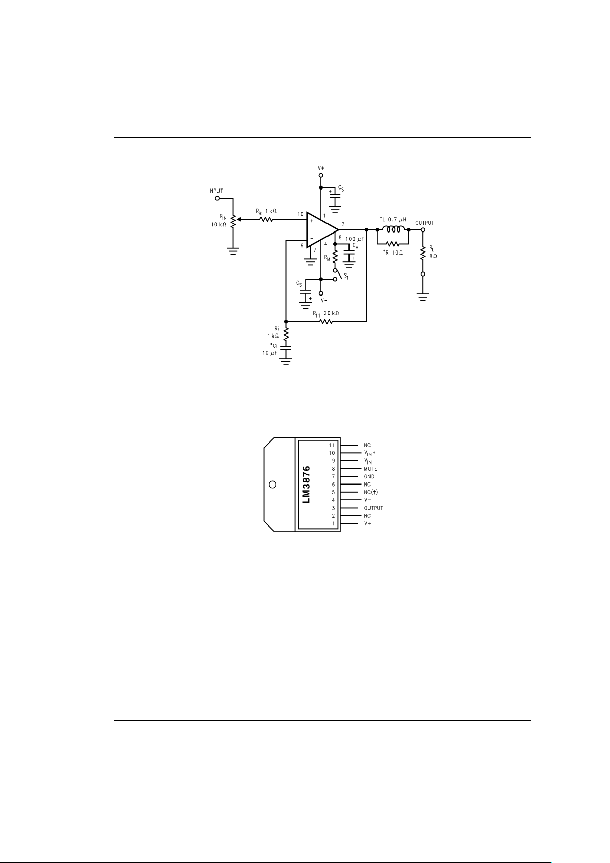
Typical Application
Connection Diagram
DS011832-1
*Optional components dependent upon specific design requirements. Refer to the External Components Description section for a component functional
description.
FIGURE 1. Typical Audio Amplifier Application Circuit
Plastic Package (Note 11)
DS011832-2
†
Connect Pin 5 to V+for Compatibility with LM3886.
Top View
Order Number LM3876T
or LM3876TF
See NS Package Number TA11B for
Staggered Lead Non-Isolated
Package or TF11B for
Staggered Lead Isolated Package
www.national.com 2
Absolute Maximum Ratings (Notes 4, 5)
If Military/Aerospace specified devices are required,
please contact the National Semiconductor Sales Office/
Distributors for availability and specifications.
Supply Voltage |V
+
|+|V−| (No Signal) 94V
Supply Voltage |V
+
|+|V−| (Input Signal) 84V
Common Mode Input Voltage (V
+
or V−) and
|V
+
|+|V−|≤80V
Differential Input Voltage 60V
Output Current Internally Limited
Power Dissipation (Note 6) 125W
ESD Susceptibility (Note 7) 3000V
Junction Temperature (Note 8) 150˚C
Soldering Information
T Package (10 seconds) 260˚C
Storage Temperature −40˚C to +150˚C
Thermal Resistance
θ
JC
1˚C/W
θ
JA
43˚C/W
Operating Ratings (Notes 4, 5)
Temperature Range
T
MIN
≤ TA≤ T
MAX
−20˚C ≤ TA≤ +85˚C
Supply Voltage |V
+
|+|V−| 24V to 84V
Note 1: Operation is guaranteedup to 84V,however,distortion may beintroduced from SPiKe Protection Circuitry when operating above 70V if proper
thermal considerations are not taken into account. Refer to the Thermal
Considerations section for more information.
(See SPiKe Protection Response)
Electrical Characteristics (Notes 4, 5)
The following specifications apply for V
+
=
+35V, V
−
=
−35V, I
MUTE
=
−0.5 mA with R
L
=
8Ω unless otherwise specified. Limits
apply for T
A
=
25˚C.
Symbol Parameter Conditions LM3876 Units
(Limits)
Typical Limit
(Note 9) (Note 10)
|V
+
|+|V−| Power Supply Voltage (Note 13) V
pin7
−V−≥9V 18 24 V (min)
84 V (max)
A
M
Mute Attenuation Pin 8 Open or at 0V, Mute: On
Current out of Pin 8
>
0.5 mA, 120 80 dB (min)
Mute: Off
P
O
(Note 3)
Output Power (Continuous Average) THD + N=0.1%(max) 56 40 W (min)
f=1 kHz; f=20 kHz
Peak P
O
Instantaneous Peak Output Power 100 W
THD + N Total Harmonic Distortion Plus Noise 40W, 20 Hz ≤ f ≤ 20 kHz 0.06
%
A
V
=
26 dB
SR
(Note 3)
Slew Rate (Note 12) V
IN
=
1.2 Vrms, f=10 kHz,
11 5
V/µs
(min)
Square-Wave, R
L
=
2kΩ
I
+
(Note 2) Total Quiescent Power Supply
Current
V
CM
=
0V, V
o
=
0V, I
o
=
0A, I
mute
=
0A 30 70 mA (max)
V
OS
(Note 2)
Input Offset Voltage V
CM
=
0V, I
o
=
0 mA 1 15 mV (max)
I
B
Input Bias Current V
CM
=
0V, I
o
=
0 mA 0.2 1 µA (max)
I
OS
Input Offset Current V
CM
=
0V, I
o
=
0 mA 0.01 0.2 µA (max)
I
o
Output Current Limit |V+|=|V−|=12V, t
ON
=
10 ms, V
O
=
0V 6 4 A (min)
V
od
(Note 2)
Output Dropout Voltage (Note 14) |V
+
–VO|, V
+
=
20V, I
o
=
+100 mA 1.6 5 V (max)
|V
O
–V−|, V
−
=
−20V, I
o
=
−100 mA 2.7 5 V (max)
PSRR
(Note 2)
Power Supply Rejection Ratio V
+
=
40V to 20V, V
−
=
−40V, 120 85 dB (min)
V
CM
=
0V, I
o
=
0mA
V
+
=
40V, V
−
=
−40V to −20V, 120 85 dB (min)
V
CM
=
0V, I
o
=
0mA
CMRR
(Note 2)
Common Mode Rejection Ratio V
+
=
60V to 20V, V
−
=
−20V to −60V, 120 80 dB (min)
V
CM
=
20V to −20V, I
o
=
0mA
A
VOL
(Note 2)
Open Loop Voltage Gain |V
+
|=|V−|=40V, R
L
=
2kΩ,∆V
O
=
60V 120 90 dB (min)
GBWP Gain-Bandwidth Product |V
+
|=|V−|=40V 8 2 MHz
(min)
f
O
=
100 kHz, V
IN
=
50 mVrms
www.national.com3
Electrical Characteristics (Notes 4, 5) (Continued)
The following specifications apply for V
+
=
+35V, V
−
=
−35V, I
MUTE
=
−0.5 mA with R
L
=
8Ω unless otherwise specified. Limits
apply for T
A
=
25˚C.
Symbol Parameter Conditions LM3876 Units
(Limits)
Typical Limit
(Note 9) (Note 10)
e
IN
(Note 3)
Input Noise IHF— A Weighting Filter 2.0 8 µV (max)
R
IN
=
600Ω (Input Referred)
SNR Signal-to-Noise Ratio P
O
=
1W, A-Weighted, 98 dB
Measured at 1 kHz, R
S
=
25Ω
P
O
=
40W, A-Weighted, 114 dB
Measured at 1 kHz, R
S
=
25Ω
Ppk=100W, A-Weighted, 122 dB
Measured at 1 kHz, R
S
=
25Ω
IMD Intermodulation Distortion Test 60 Hz, 7 kHz, 4:1 (SMPTE) 0.004
%
60 Hz, 7 kHz, 1:1 (SMPTE) 0.006
Note 2: DC Electrical Test; refer to Test Circuit#1.
Note 3: AC Electrical Test; refer to Test Circuit
#
2.
Note 4: All voltages are measured with respect to the GND pin (pin 7), unless otherwise specified.
Note 5: Absolute Maximum Ratings indicate limits beyond which damage to the device may occur. Operating Ratings indicate conditions for which the device is
functional, but do not guarantee specific performance limits. Electrical Characteristics state DC and AC electrical specifications under particular test conditions which
guarantee specific performance limits. This assumes that the device is within the Operating Ratings. Specifications are not guaranteed for parameters where no limit
is given, however, the typical value is a good indication of device performance.
Note 6: For operating at case temperatures above 25˚C, the device must be derated based on a 150˚C maximum junction temperature and a thermal resistance of
θ
JC
=
1.0 ˚C/W (junction to case). Refer to the Thermal Resistance figure in the Application Information section under Thermal Considerations.
Note 7: Human body model, 100 pF discharged through a 1.5 kΩ resistor.
Note 8: The operating junction temperature maximum is 150˚C, however, the instantaneous Safe Operating Area temperature is 250˚C.
Note 9: Typicals are measured at 25˚C and represent the parametric norm.
Note 10: Limits are guaranteed to National’s AOQL (Average Outgoing Quality Level).
Note 11: The LM3876T package TA11B is a non-isolated package, setting the tab of the device and the heat sink at V
−
potential when the LM3876 is directly
mounted to the heat sink using only thermal compound. If a mica washer is used in addition to thermal compound, θ
CS
(case to sink) is increased, but the heat sink
will be isolated from V
−
.
Note 12: The feedback compensation network limits the bandwidth of the closed-loop response and so the slew rate will be reduced due to the high frequency
roll-off. Without feedback compensation, the slew rate is typically 16V/µs.
Note 13: V
−
must have at least −9V at its pin with reference to ground in order for the under-voltage protection circuitry to be disabled.
Note 14: The output dropout voltage is the supply voltage minus the clipping voltage. Refer to the Clipping Voltage vs Supply Voltage graph in the Typical Performance Characteristics section.
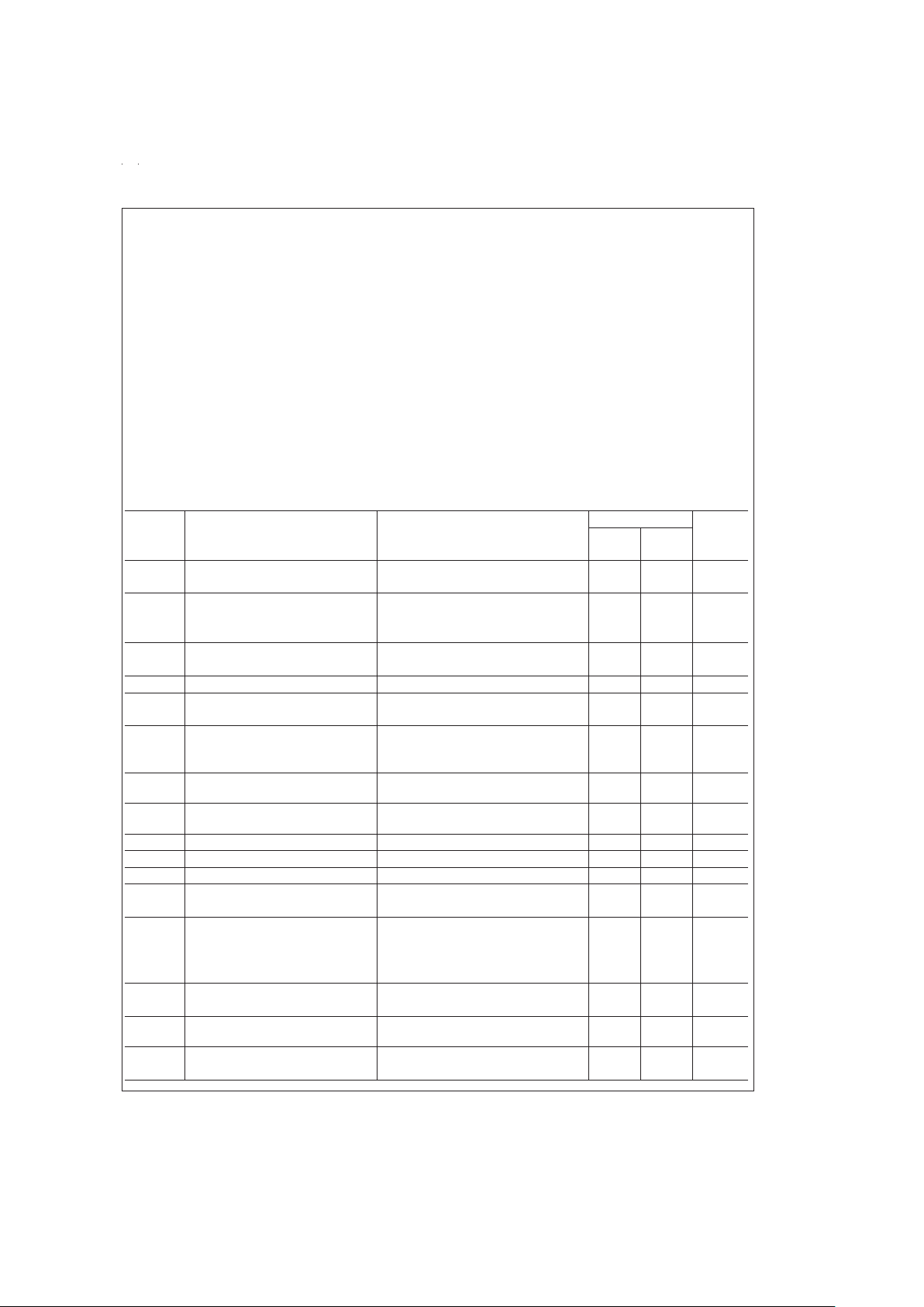
Test Circuit#1 (DC Electrical Test Circuit)
DS011832-3
www.national.com 4
Test Circuit#2 (AC Electrical Test Circuit)
Single Supply Application Circuit
DS011832-4
DS011832-5
*
Optional components dependent upon specific design requirements. Refer to the External
Components Description section for a component functional description.
FIGURE 2. Typical Single Supply Audio Amplifier Application Circuit
www.national.com5
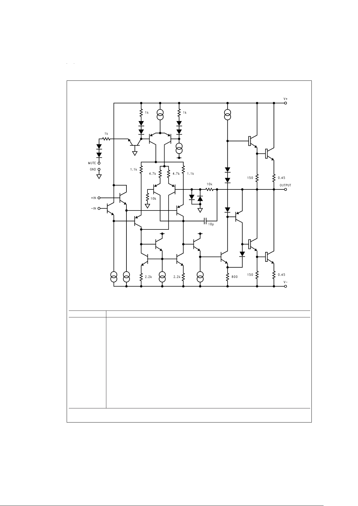
Equivalent Schematic (excluding active protection circuitry)
External Components Description
(
Figures 1, 2
)
Components Functional Description
1. R
IN
Acts as a volume control by setting the voltage level allowed to the amplifier’s input terminals.
2. R
A
Provides DC voltage biasing for the single supply operation and bias current for the positive input terminal.
3. C
A
Provides bias filtering.
4. C Provides AC coupling at the input and output of the amplifier for single supply operation.
5. R
B
Prevents currents from entering the amplifier’s non-inverting input which may be passed through to the load
upon power-down of the system due to the low input impedance of the circuitry when the under-voltage
circuitry is off. This phenomenon occurs when the supply voltages are below 1.5V.
6. C
C
(Note 15)
Reduces the gain (bandwidth of the amplifier) at high frequencies to avoid quasi-saturation oscillations of
the output transistor. The capacitor also suppresses external electromagnetic switching noise created from
fluorescent lamps.
7. Ri Inverting input resistance to provide AC Gain in conjunction with R
f1
.
8. Ci
(Note 15)
Feedback capacitor. Ensures unity gain at DC. Also a low frequency pole (highpass roll-off) at:
f
c
=
1/(2πRi Ci)
9. R
f1
Feedback resistance to provide AC Gain in conjunction with Ri.
DS011832-6
www.national.com 6
 Loading...