

Datasheet LM3813M-7.0, LM3813M-1.0, LM3812MX-7.0, LM3812M-7.0, LM3812M-1.0 Datasheet (NSC)
...
June 1999
LM3812/LM3813
Precision Current Gauge IC with Ultra Low Loss Sense
Element and PWM Output
LM3812/LM3813 Precision Current Gauge IC with Ultra Low Loss Sense Element and PWM
Output
General Description
The LM3812/LM3813 Current Gauges provide easy to use
precision current measurement with virtually zero insertion
loss (typically 0.004Ω). The LM3812 is used for high-side
sensing and the LM3813 is used for low-side sensing.
A Delta Sigma analog to digital converter is incorporated to
precisely measure the current and to provide a current averaging function. Current is averaged over 50 msec time periods in order to provide immunity to current spikes. The ICs
have a pulse-widthmodulated (PWM) output which indicates
the current magnitude and direction. The shutdown pin can
be used to inhibit false triggering during start-up, or to enter
a low quiescent current mode.
The LM3812 and LM3813 are factory-set in two different current options. The sense range is −1A to +1A or −7A to +7A.
The sampling interval for these parts is 50ms. If faster sampling is desired, please refer to the data sheets for the part
numbers LM3814 and LM3815.
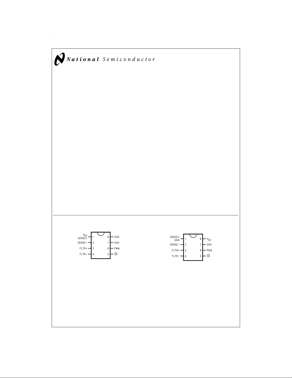
Connection Diagrams
Key Specifications
n Ultra low insertion loss (typically 0.004Ω)
n 2V to 5.25V supply range
±
n
2%accuracy at room temperature (includes accuracy
of the internal sense element) (LM3812-1.0,
LM3813-1.0)
n Low quiescent current in shutdown mode (typically
2.5 µA)
n 50 msec sampling interval
Features
n No external sense element required
n PWM output indicates the current magnitude and
direction
n PWM output can be interfaced with microprocessors
n Precision ∆Σ current-sense technique
n Low temperature sensitivity
n Internal filtering rejects false trips
n Internal Power-On-Reset (POR)
Applications
n Battery charge/discharge gauge
n Motion control diagnostics
n Power supply load monitoring and management
n Resettable smart fuse
DS100122-1
Top View
LM3812
for High-Side Sensing
© 1999 National Semiconductor Corporation DS100122 www.national.com
Top View
LM3813
for Low-Side Sensing
DS100122-3
Ordering Information
Order No.
LM3812M-1.0
LM3812MX-1.0
LM3812M-7.0
LM3812MX-7.0
LM3813M-1.0
LM3813MX-1.0
LM3813M-7.0
LM3813MX-7.0
#
Suffix M indicates that the part is available in Surface Mount package. Suffix X indicates that the part is available in 2.5k units
on Tape and Reel.
*
Current is sampled over a fixed interval. The average current during this interval is indicated by the duty cycle of the PWM output
during next interval.
‡
The Package code M08A is internal to National Semiconductor and indicates an 8-lead surface mount package, SO-8.
#
Sense
Range
±
±
±
±
±
±
±
±
Sampling
Interval
1A 50 ms High-side M08A SO-8 95 units in Rails
1A 50 ms High-side M08A SO-8 2.5k units on Tape and Reel
7A 50 ms High-side M08A SO-8 95 units in Rails
7A 50 ms High-side M08A SO-8 2.5k units on Tape and Reel
1A 50 ms Low-side M08A SO-8 95 units in Rails
1A 50 ms Low-side M08A SO-8 2.5k units on Tape and Reel
7A 50 ms Low-side M08A SO-8 95 units in Rails
7A 50 ms Low-side M08A SO-8 2.5k units on Tape and Reel
Sensing
*
Method
NS
Package
Number
Package
‡
Type Supplied As:
Pin Description (High-Side, LM3812)
Pin Name Function
1 SENSE+, V
2 SENSE− Low side of internal current sense.
3 FLTR+ Filter input — provides anti-aliasing for delta sigma modulator.
4 FLTR− Filter input.
5SD
6 PWM PWM output indicates the current magnitude and direction.
7 GND Ground
8 GND Ground
DD
High side of internal current sense, also supply voltage.
Shutdown pin. Connected to VDDthrough a pull up resistor for normal operation.
When low, the IC goes into a low current mode (typically 3 µA).
Pin Description (Low-Side, LM3813)
Pin Name Function
1 SENSE+, GND High side of internal current sense, also ground.
2 SENSE− Low side of internal current sense.
3 FLTR+ Filter input – provides anti-aliasing for delta sigma modulator.
4 FLTR− Filter input.
5SD
6 PWM PWM output indicates the current magnitude and direction.
7 GND Ground
8V
www.national.com 2
DD
Shutdown pin. Connected to VDDthrough a pull up resistor for normal operation.
When low, the IC goes into a low current mode (typically 3 µA).
VDD(supply)
Absolute Maximum Ratings (Note 1)
If Military/Aerospace specified devices are required,
please contact the National Semiconductor Sales Office/
Distributors for availability and specifications.
Absolute Maximum Supply Voltage 5.5V
Power Dissipation (Note 2)
ESD Susceptibility (Note 3) 1.5 kV
Sense Current (peak, for 200 msec) (Note 4) 10A
Maximum Junction Temperature 150˚C
Storage Temperature −65˚C to +150˚C
Lead Temperature (Soldering, 10 sec) 260˚C
Operating Ratings (Note 1)
Input Voltage 2.0V to 5.25V
Sense Current (continuous) (Note 4) 7A
Junction Temperature Range −40˚C to +125˚C
Sink Current for PWM pin 1mA
Voltage on Pin 5 5.25V
Electrical Characteristics
LM3812-1.0, LM3813-1.0
=
V
5.0V for the following specifications. Supply bypass capacitor is 1 µF and filter capacitor is 0.1 µF.
DD
Symbol Parameter Conditions
I
e
ACC
Average Current Accuracy
(Note 7)
n
Effective Output Noise (rms) 2 mA
at 0.9A current 0.9
(Note 5)
LM3812-7.0, LM3813-7.0
=
V
5.0V for the following specifications. Supply bypass capacitor is 1 µF and filter capacitor is 0.1 µF.
DD
Symbol Parameter Conditions
I
e
ACC
Average Current Accuracy
(Note 7)
n
Effective Output Noise (rms) 20 mA
at 2.5A current (Note 8) 2.5 A
(Note 5)
Typ
Typ
Limit
(Note 6)
Units
A
0.882 / 0.864 A (min)
0.918 / 0.936 A (max)
Limit
(Note 6)
Units
2.400 / 2.350 A (min)
2.600 / 2.650 A (max)
Common Device Parameters
Unless otherwise specified, V
0.1 µF.
Symbol Parameter Conditions
I
Q1
I
Q2
D
RES
t
S
f
P
V
TH
V
TL
Quiescent Current Normal Mode, SD=high 100 µA
Quiescent Current Shutdown Mode, SD=low 2.5 µA
PWM Resolution 0.1
Sampling Time 52 ms
Frequency of PWM Waveform 20 Hz
Threshold High Level for SD 1.2 V
Threshold Low Level for SD 1.3 V
=
5.0V for the following specifications. Supply bypass capacitor is 1 µF and filter capacitor is
DD
Typ
(Note 5)
Limit
(Note 6)
Units
160 µA (max)
10 µA (max)
40 ms (min)
80 ms (max)
12.5 Hz (min)
25 Hz (max)
1.8 V (min)
0.7 V (max)
www.national.com3
%
Common Device Parameters (Continued)
Unless otherwise specified, V
0.1 µF.
Symbol Parameter Conditions
V
OH
V
OL
P
I
Note 1: Absolute Maximum Ratings indicate limits beyond which damage to the device may occur. Operating Ratings indicate conditions for which the device is intended to be functional, but do not guarantee specific performance limits. For guaranteed specifications and test conditions, see Electrical Characteristics. The guaranteed specifications apply only for the test conditions listed. Some performance characteristics may degrade when the device is not operated under the listed test
conditions.
Note 2: At elevated temperatures, devices must be derated based on package thermal resistance. The device in the surface-mount package must be derated at
θ
Note 3: The human body model is a 100 pF capacitor discharged through a 1.5 kΩ resistor into each pin.
Note 4: The absolute maximum peak and continuous currents specified are not tested. These specifications are dependent on the θ
package.
Note 5: Typical numbers are at 25˚C and represent the most likely parametric norm. Specifications in standard type face are for T
type apply over full operating temperature ranges.
Note 6: Limits are 100%production tested at 25˚C. Limits over the operating temperature range are guaranteed through correlation using Statistical Quality Control
(SQC) methods. The limits are used to calculate National’s Averaging Outgoing Quality Level (AOQL).
Note 7: There is a variation in accuracy over time due to thermal effects. Please refer to the “PWM Output and Current Accuracy” section for more information.
Note 8: The PWM accuracy for LM3812-7.0 and LM3813-7.0 depends on the amount of copper area under pins 1 and 2, and the layout. Please refer to the “PWM
Output and Current Accuracy” section for more information.
Note 9: The tolerance of the internal lead frame resistor is corrected internally. The temperature coefficient of this resistor is 2600 ppm/˚C.
Logic High Level for PWM Load current=1 mA, 2V ≤ VDD≤
Logic Low Level for PWM Sink current=1 mA, 2V ≤ VDD≤
Insertion Loss I
=
150˚C/W (typically), junction-to-ambient.
JA
=
5.0V for the following specifications. Supply bypass capacitor is 1 µF and filter capacitor is
DD
Typ
(Note 5)
Limit
(Note 6)
VDD− 0.05
5.25V
− 0.2
V
DD
0.04 V
5.25V
SENSE
=
1A (Note 9) 0.004 Ω
0.2 V (max)
, which is 150˚C/W for the S08
JA
=
25˚C and those with boldface
J
Units
V (min)
V
www.national.com 4
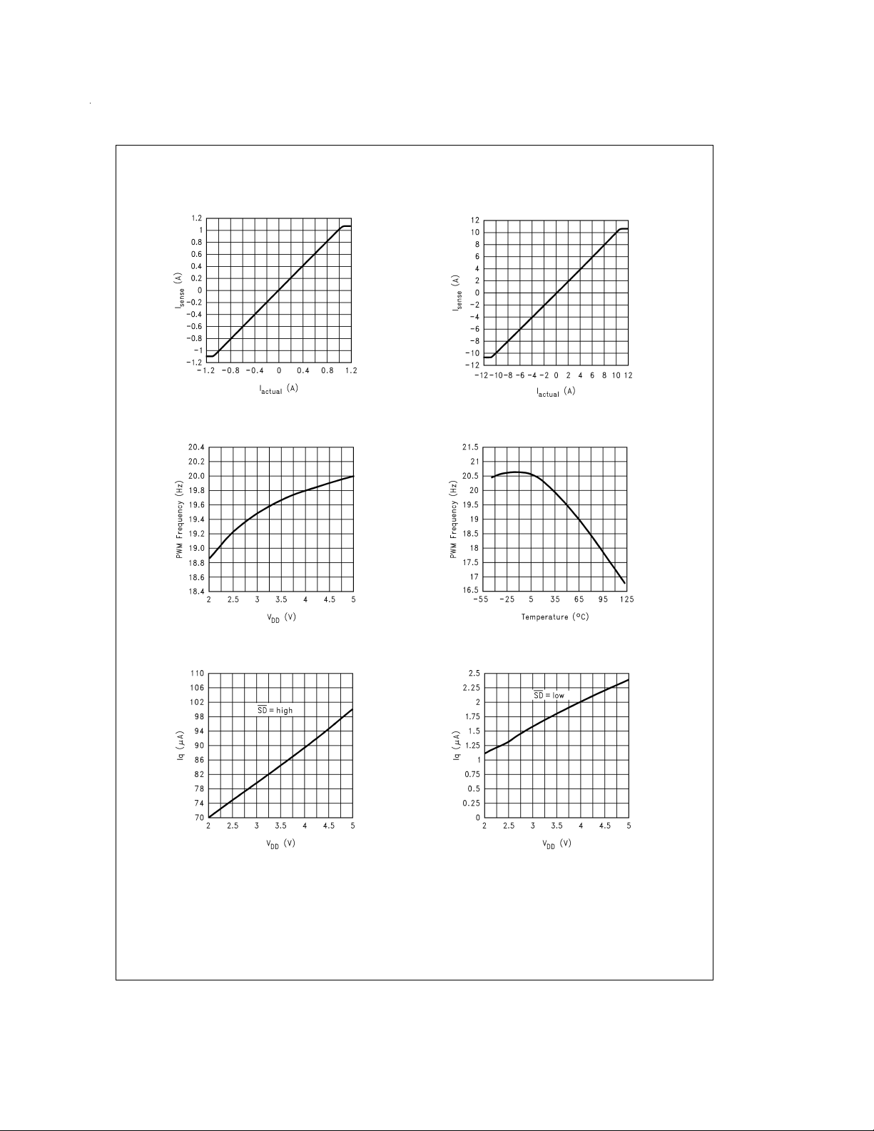
Typical Performance Characteristics Supply bypass capacitor is 0.1 µF and filter capacitor is 0.1 µF.
Measured Current vs Actual Current
(LM3812-1.0 and LM3813-1.0)
PWM Frequency vs Supply Voltage
DS100122-15
Measured Current vs Actual Current
(LM3812-7.0 and LM3813-7.0)
DS100122-24
PWM Frequency vs Temperature
Operating Current vs Supply Voltage
DS100122-13
DS100122-18
DS100122-16
Shutdown Current vs Supply Voltage
DS100122-19
www.national.com5

Typical Performance Characteristics Supply bypass capacitor is 0.1 µF and filter capacitor is
0.1 µF. (Continued)
Operating Current vs Temperature
Current vs Duty Cycle
DS100122-20
Shutdown Current vs Temperature
DS100122-21
Accuracy vs Supply Voltage
DS100122-22
Accuracy vs Temperature (LM3812-1.0 and LM3813-1.0)
DS100122-29
www.national.com 6
DS100122-28
Accuracy vs Temperature (LM3812-7.0 and LM3813-7.0)
DS100122-30

Typical Performance Characteristics Supply bypass capacitor is 0.1 µF and filter capacitor is
0.1 µF. (Continued)
Error vs Current (LM3812-1.0 and LM3813-1.0)
(Note 10)
DS100122-27
Note 10: These curves represent a statistical average such that the noise is insignificant.
Error vs Current (LM3812-7.0 and LM3813-7.0)
(Note 10)
DS100122-31
Typical Application Circuits In the application circuits, the 0.1 µF ceramic capacitor between pins 1 and 8
is used for bypassing, and the 0.1 µF ceramic capacitor between pins 3 and 4 is used for filtering. Shutdown (SD) is tied to
VDDthrough a 10 kΩ resistor.
FIGURE 1. High Side Sense
FIGURE 2. Low Side Sense
DS100122-5
DS100122-6
www.national.com7

Typical Application Circuits In the application circuits, the 0.1 µF ceramic capacitor between pins 1 and 8
is used for bypassing, and the 0.1 µF ceramic capacitor between pins 3 and 4 is used for filtering. Shutdown (SD) is tied to
VDDthrough a 10 kΩ resistor. (Continued)
DS100122-7
FIGURE 3. Paralleling LM3812 for Higher Load Current
where D1is the duty cycle of PWM1 and D2is the duty cycle of PWM2.
Please refer to the Product Operation section for more information.
I
TOTAL
=
2.2(D
−0.5)I
1
+ 2.2(D2−0.5)I
MAX
MAX
FIGURE 4. High Voltage Operation — VINGreater Than 5.25V (High Side Sense)
(PWM output is referred to Pin 7)
www.national.com 8
DS100122-8

Typical Application Circuits In the application circuits, the 0.1 µF ceramic capacitor between pins 1 and 8
is used for bypassing, and the 0.1 µF ceramic capacitor between pins 3 and 4 is used for filtering. Shutdown (SD) is tied to
VDDthrough a 10 kΩ resistor. (Continued)
DS100122-9
FIGURE 5. High Voltage Operation — VINGreater Than 5.25V (Low Side Sense)
www.national.com9

Product Operation
The current is sampled by the delta-sigma modulator, as illustrated in
delta-sigma modulator is digitally filtered. The digital output
is then compared to the output of a digital ramp generator.
This produces a PWM output. The duty cycle of the PWM
output is proportional to the amount of current flowing.Aduty
cycle of 50%indicates zero current flow. If the current is flowing in positive direction, the duty cycle will be greater than
50%. Conversely, the duty cycle will be less than 50%for
currents flowing in the negative direction. A duty cycle of
95.5%(4.5%) indicates the current is at I
can sense currents from −I
1A or 10A. The sense current is given by:
where D is the duty cycle of the PWM waveform, and I
the full scale current (1A or 10A). Similarly, the duty cycle is
given by:
For quick reference, see the Conversion Tables in
and
Table 2
Figure 6
I
SENSE
D=[I
.
. The pulse density output of the
(−I
MAX
=
2.2 (D−0.5)(I
SENSE
/(2.2 I
to +I
MAX
MAX
)] + 0.5
MAX
. Options for I
MAX
). The IC
MAX
MAX
)
MAX
Table 1
are
The user should note that, while the LM3812-7.0/
LM3813-7.0 will read 10A full scale, it is rated for 10A operation for a duration of no more than 200 msec, and 7A
operation continuously.
In this IC, the current is averaged over 50 msec time slots.
Hence, momentary current surges of less than 50 msec are
tolerated.
This is a sampled data system which requires an
anti-aliasing filter, provided by the filter capacitor.
The delta-sigma modulator converts the sensed current to
the digital domain. This allows digital filtering, and provides
immunity to current and noise spikes. This type of filtering
would be difficult or impossible to accomplish on an IC with
is
analog components.
When ordering, the user has to specify whether the part is
being used for low-side or high-side sense. The user also
needs to specify the full scale value. See the Ordering Information table for details.
FIGURE 6. Functional block diagram of LM3812 and LM3813
www.national.com 10
DS100122-10

PWM Output and Current
Accuracy
Offset
The PWM output is quantized to 1024 levels. Therefore, the
duty cycle can change only in increments of 1/1024.
There is a one-half (0.5) quantization cycle delay in the output of the PWM circuitry. That is to say that instead of a duty
cycle of N/1024, the duty cycle actually is (N+
The quantization error can be corrected for if a more precise
result is desired. To correct for this error, simply subtract
1/2048 from the measured duty cycle.
The extra half cycle delay will show up as a DC offset of
bit if it is not corrected for.This is approximately 1.1 mA for 1
Amp parts, and 11 mA for 7 Amp parts.
Jitter
In addition to quantization, the duty cycle will contain some
jitter. The jitter is quite small (for example, the standard deviation of jitter is only 0.1%for the LM3812/13-1.0). Statistically the jitter can cause an error in a current sample. Because the jitter is a random variable, the mean and standard
deviation are used. The mean, or average value, of the jitter
is zero. The standard deviation (0.1%) can be used to define
the peak error caused from jitter.
The “crest factor” has often been used to define the maximum error caused by jitter. The crest factor defines a limit
within which 99.7%of the samples fall. The crest factor is de-
±
fined as
0.3%error in the duty cycle.
Since the jitter is a random variable, averaging multiple outputs will reduce the effective jitter. Obeying statistical laws,
the jitter is reduced by the square root of the number of readings that are averaged. For example, if four readings of the
duty cycle are averaged, the resulting jitter (and crest factor)
are reduced by a factor of two.
Jitter and Noise
Jitter in the PWM output appears as noise in the current
measurement. The Electrical Characteristics show noise
measured in current RMS (root mean square). Arbitrarily one
could specify PWM jitter, as opposed to noise. In either case
the effect results in a random error in an individual current
measurement.
Noise, just like jitter, can be reduced by averaging many
readings. The RMS value of the noise corresponds to one
standard deviation. The “crest factor” can be calculated in
terms of current, and is equal to
±
3 sigma (RMS value of the
noise).
Noise will also be reduced by averaging multiple readings,
and follows the statistical laws of a random variable.
Accuracy of 7A Versions
The graph of
Figure 7
shows two possible responses to a 7A
current step. The flat response shows basically a 7A level
with some noise. This is what is possible with a good thick
trace and a good thermal connection to the IC on the sense
pins.
The second trace that asymptotically approaches a higher
value shows what can happen under extremely poor thermal
conditions. Here a very small wire connects the IC to the current source. The very small wire does not allow heat in the
sense resistor to dissipate. Hence, as the sense resistor
heats up, a temperature difference between the sense ele-
1
⁄2)/1024.
ment and the die gets larger, and an error develops. Eventually the temperature difference reaches steady state, which
accounts for the under-damped exponential response.
1
⁄
2
DS100122-23
FIGURE 7. Transient Response to 7 Amp Step Current
Accuracy versus Noise
The graph shown in
±
of
1 Ampere current gauges. In this graph, the horizontal
Figure 8
illustrates the typical response
axis indicates time, and the vertical axis indicates measured
current (the PWM duty cycle has been converted to current).
The graph was generated for an actual current of 500 mA.
The difference between successive readings manifests itself
as jitter in the PWM output or noise in the current measurement (when duty cycle of the PWM output is converted to
current).
The accuracy of the measurement depends on the noise in
the current waveform. The accuracy can be improved by averaging several outputs. Although there is variation in successive readings, a very accurate measurement can be obtained by averaging the readings. For example, on
averaging the readings shown in this example, the average
current measurement is 502.3 mA (
Figure 8
). This value is
very close to the actual value of 500 mA. Moreover, the accuracy depends on the number of readings that are
averaged.
DS100122-26
FIGURE 8. Typical Response of LM3812-1.0/LM3813-1.0
www.national.com11

Look-Up Tables
The following tables show how to convert the duty cycle of
the PWM output to a current value, and vice versa. The
TABLE 1. Current to Duty Cycle Conversion Table
Sense Current
*
(Amps)
1.00 95.5 -1.00 4.5
0.95 93.2 -0.95 6.8
0.90 90.9 -0.90 9.1
0.85 88.6 -0.85 11.4
0.80 86.4 -0.80 13.6
0.75 84.1 -0.75 15.9
0.70 81.8 -0.70 18.2
0.65 79.5 -0.65 20.5
0.60 77.3 -0.60 22.7
0.55 75.0 -0.55 25.0
0.50 72.7 -0.50 27.3
0.45 70.5 -0.45 29.5
0.40 68.2 -0.40 31.8
0.35 65.9 -0.35 34.1
0.30 63.6 -0.30 36.4
0.25 61.4 -0.25 38.6
0.20 59.1 -0.20 40.9
0.15 56.8 -0.15 43.2
0.10 54.5 -0.10 45.5
0.05 52.3 -0.05 47.7
0.00 50.0 -0.00 50.0
*
Maximum Sense Current=1.0 Amps for LM3812-1.0 and LM3813-1.0.
The sense current should be multiplied by 10 for LM3812-7.0 and LM3813-7.0.
Duty Cycle
(%)
quantization error of
1
⁄2bit is not shown in these tables.
Please see the “PWM Output and Current Accuracy” section
for more details.
Sense Current
*
(Amps)
Duty Cycle
(%)
www.national.com 12

Look-Up Tables (Continued)
TABLE 2. Duty Cycle to Current Conversion Table
Duty Cycle
(%)
95.5 0.990 50.0 -0.000
92.5 0.935 47.5 -0.055
90.0 0.880 45.0 -0.110
87.5 0.825 42.5 -0.165
85.0 0.770 40.0 -0.220
82.5 0.715 37.5 -0.275
80.0 0.660 35.0 -0.330
77.5 0.605 32.5 -0.385
75.0 0.550 30.0 -0.440
72.5 0.495 27.5 -0.495
70.0 0.440 25.0 -0.550
67.5 0.385 22.5 -0.605
65.0 0.330 20.0 -0.660
62.5 0.275 17.5 -0.715
60.0 0.220 15.0 -0.770
57.5 0.165 12.5 -0.825
55.0 0.110 10.0 -0.880
52.5 0.055 7.5 -0.935
50.0 0.000 5.0 -0.990
*
Maximum Sense Current=1.0 Amps for LM3812-1.0 and LM3813-1.0.
The sense current should be multiplied by 10 for LM3812-7.0 and LM3813-7.0.
Timing Diagram
Sense Current
(Amps)
Duty Cycle
(%)
Sense Current
(Amps)
Duty cycle of the PWM waveform during any sampling interval indicates the current magnitude (average) and direction during the previous sampling interval.
DS100122-11
FIGURE 9. Typical Timing Diagram for Mostly Positive Current
www.national.com13

Physical Dimensions inches (millimeters) unless otherwise noted
Output
8-lead (0.150" Wide) Molded Small Outline Package
See Ordering Information table for Order Numbers
NS Package Number M08A
LIFE SUPPORT POLICY
NATIONAL’S PRODUCTS ARE NOT AUTHORIZED FOR USE AS CRITICAL COMPONENTS IN LIFE SUPPORT
DEVICES OR SYSTEMS WITHOUT THE EXPRESS WRITTEN APPROVAL OF THE PRESIDENT AND GENERAL
COUNSEL OF NATIONAL SEMICONDUCTOR CORPORATION. As used herein:
1. Life support devices or systems are devices or
systems which, (a) are intended for surgical implant
into the body, or (b) support or sustain life, and
whose failure to perform when properly used in
accordance with instructions for use provided in the
2. A critical component is any component of a life
support device or system whose failure to perform
can be reasonably expected to cause the failure of
the life support device or system, or to affect its
safety or effectiveness.
labeling, can be reasonably expected to result in a
significant injury to the user.
National Semiconductor
LM3812/LM3813 Precision Current Gauge IC with Ultra Low Loss Sense Element and PWM
Corporation
Americas
Tel: 1-800-272-9959
Fax: 1-800-737-7018
Email: support@nsc.com
www.national.com
National does not assume any responsibility for use of any circuitry described, no circuit patent licenses are implied and National reserves the right at any time without notice to change said circuitry and specifications.
National Semiconductor
Europe
Fax: +49 (0) 1 80-530 85 86
Email: europe.support@nsc.com
Deutsch Tel: +49 (0) 1 80-530 85 85
English Tel: +49 (0) 1 80-532 78 32
Français Tel: +49 (0) 1 80-532 93 58
Italiano Tel: +49 (0) 1 80-534 16 80
National Semiconductor
Asia Pacific Customer
Response Group
Tel: 65-2544466
Fax: 65-2504466
Email: sea.support@nsc.com
National Semiconductor
Japan Ltd.
Tel: 81-3-5639-7560
Fax: 81-3-5639-7507
 Loading...